| Citation: |
Zhaojun Suo, Linwang Wang, Shushen Li, Junwei Luo. Clarifying the atomic origin of electron killers in β-Ga2O3 from the first-principles study of electron capture rates[J]. Journal of Semiconductors, 2022, 43(11): 112801. doi: 10.1088/1674-4926/43/11/112801
****
Z J Suo, L W Wang, S S Li, J W Luo. Clarifying the atomic origin of electron killers in β-Ga2O3 from the first-principles study of electron capture rates[J]. J. Semicond, 2022, 43(11): 112801. doi: 10.1088/1674-4926/43/11/112801
|
Clarifying the atomic origin of electron killers in β-Ga2O3 from the first-principles study of electron capture rates
DOI: 10.1088/1674-4926/43/11/112801
More Information
-
Abstract
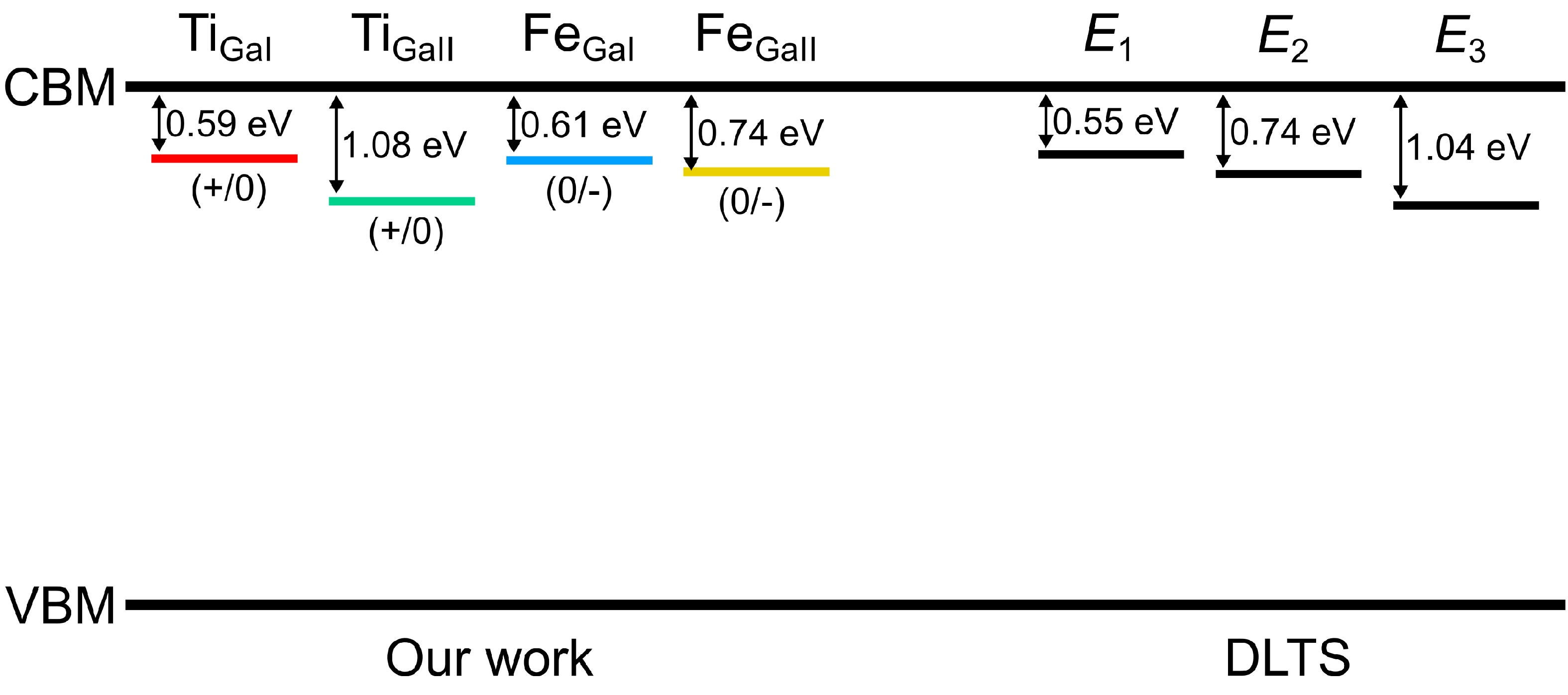
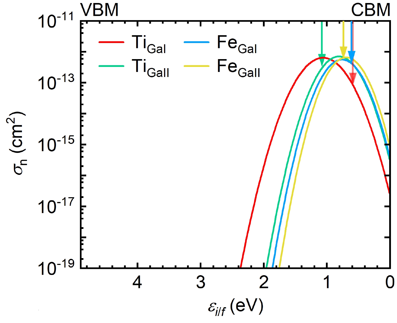
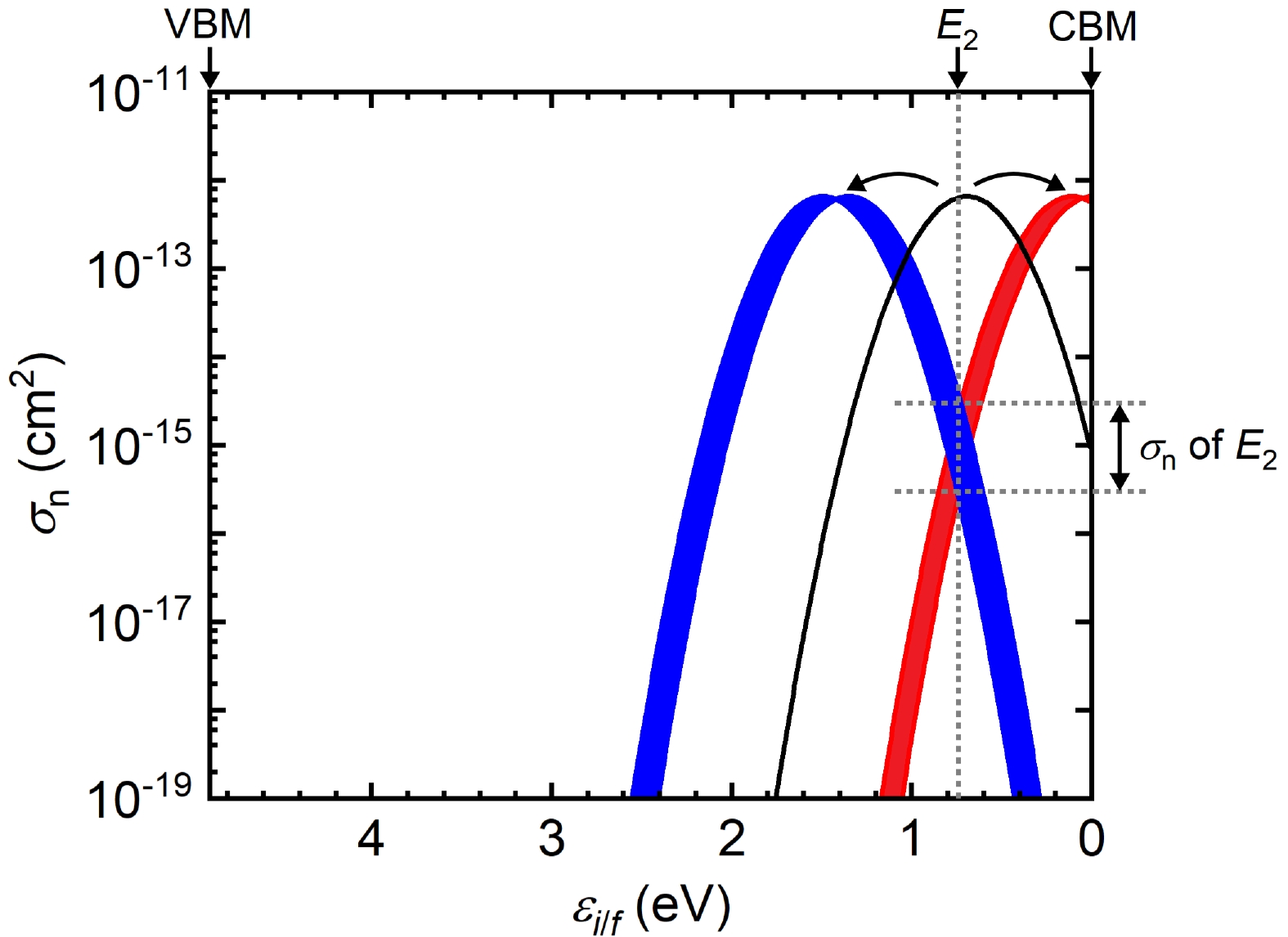
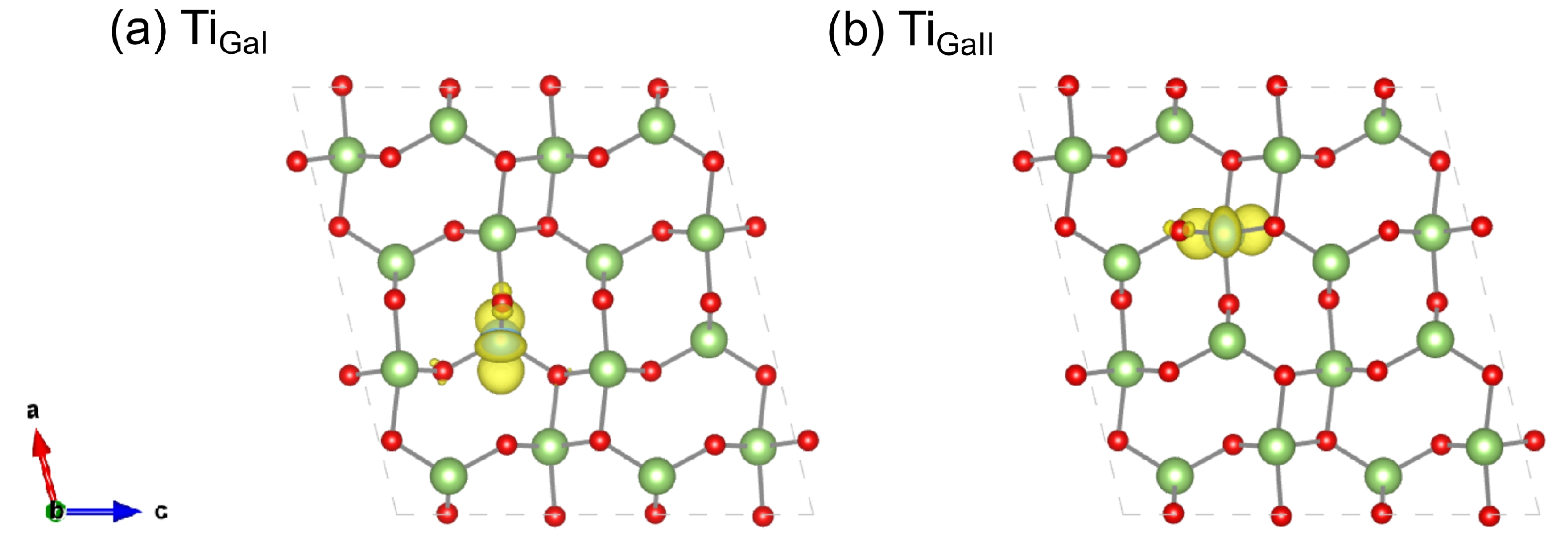
The emerging wide bandgap semiconductor$ \beta $ -Ga2O3 has attracted great interest due to its promising applications for high-power electronic devices and solar-blind ultraviolet photodetectors. Deep-level defects in$ \beta $ -Ga2O3 have been intensively studied towards improving device performance. Deep-level signatures E1, E2, and E3 with energy positions of 0.55–0.63, 0.74–0.81, and 1.01–1.10 eV below the conduction band minimum have frequently been observed and extensively investigated, but their atomic origins are still under debate. In this work, we attempt to clarify these deep-level signatures from the comparison of theoretically predicted electron capture cross-sections of suggested candidates, Ti and Fe substituting Ga on a tetrahedral site (TiGaI and FeGaI) and an octahedral site (TiGaII and FeGaII), to experimentally measured results. The first-principles approach predicted electron capture cross-sections of TiGaI and TiGaII defects are 8.56 × 10⁻¹⁴ and 2.97 × 10⁻¹³ cm2, in good agreement with the experimental values of E1 and E3 centers, respectively. We, therefore, confirmed that E1 and E3 centers are indeed associated with TiGaI and TiGaII defects, respectively. Whereas the predicted electron capture cross-sections of FeGa defect are two orders of magnitude larger than the experimental value of the E2, indicating E2 may have other origins like CGa and Gai, rather than common believed FeGa. -
References
[1] Pearton S J, Yang J C, Cary P H IV, et al. A review of Ga2O3 materials, processing, and devices. Appl Phys Rev, 2018, 5, 011301 doi: 10.1063/1.5006941[2] Higashiwaki M, Sasaki K, Murakami H, et al. Recent progress in Ga2O3 power devices. Semicond Sci Technol, 2016, 31, 034001 doi: 10.1088/0268-1242/31/3/034001[3] Gu Y X, Shi L, Luo J W, et al. Directly confirming the Z1/2 center as the electron trap in SiC through accessing the nonradiative recombination. Phys Status Solidi R, 2022, 16, 2100458 doi: 10.1002/pssr.202100458[4] Irmscher K, Galazka Z, Pietsch M, et al. Electrical properties of β-Ga2O3 single crystals grown by the Czochralski method. J Appl Phys, 2011, 110, 063720 doi: 10.1063/1.3642962[5] Farzana E, Chaiken M F, Blue T E, et al. Impact of deep level defects induced by high energy neutron radiation in β-Ga2O3. APL Mater, 2019, 7, 022502 doi: 10.1063/1.5054606[6] Polyakov A Y, Smirnov N B, Shchemerov I V, et al. Compensation and persistent photocapacitance in homoepitaxial Sn-doped β-Ga2O3. J Appl Phys, 2018, 123, 115702 doi: 10.1063/1.5025916[7] Ingebrigtsen M E, Kuznetsov A Y, Svensson B G, et al. Impact of proton irradiation on conductivity and deep level defects in β-Ga2O3. APL Mater, 2019, 7, 022510 doi: 10.1063/1.5054826[8] Ingebrigtsen M E, Varley J B, Kuznetsov A Y, et al. Iron and intrinsic deep level states in Ga2O3. Appl Phys Lett, 2018, 112, 042104 doi: 10.1063/1.5020134[9] Polyakov A Y, Smirnov N B, Shchemerov I V, et al. Point defect induced degradation of electrical properties of Ga2O3 by 10 MeV proton damage. Appl Phys Lett, 2018, 112, 032107 doi: 10.1063/1.5012993[10] Zimmermann C, Frodason Y K, Barnard A W, et al. Ti- and Fe-related charge transition levels in β-Ga2O3. Appl Phys Lett, 2020, 116, 072101 doi: 10.1063/1.5139402[11] Zimmermann C, Kalmann Frodason Y, Rønning V, et al. Combining steady-state photo-capacitance spectra with first-principles calculations: The case of Fe and Ti in β-Ga2O3. New J Phys, 2020, 22, 063033 doi: 10.1088/1367-2630/ab8e5b[12] Polyakov A Y, Smirnov N B, Shchemerov I V, et al. Defects responsible for charge carrier removal and correlation with deep level introduction in irradiated β-Ga2O3. Appl Phys Lett, 2018, 113, 092102 doi: 10.1063/1.5049130[13] Zimmermann C, Rønning V, Kalmann Frodason Y, et al. Primary intrinsic defects and their charge transition levels in β-Ga2O3. Phys Rev Mater, 2020, 4, 074605 doi: 10.1103/PhysRevMaterials.4.074605[14] Lee M H, Peterson R L. Interfacial reactions of titanium/gold ohmic contacts with Sn-doped β-Ga2O3. APL Mater, 2019, 7, 022524 doi: 10.1063/1.5054624[15] Zhang Z, Farzana E, Arehart A R, et al. Deep level defects throughout the bandgap of (010) β-Ga2O3 detected by optically and thermally stimulated defect spectroscopy. Appl Phys Lett, 2016, 108, 052105 doi: 10.1063/1.4941429[16] Jia W L, Fu J Y, Cao Z Y, et al. Fast plane wave density functional theory molecular dynamics calculations on multi-GPU machines. J Comput Phys, 2013, 251, 102 doi: 10.1016/j.jcp.2013.05.005[17] Jia W L, Cao Z Y, Wang L, et al. The analysis of a plane wave pseudopotential density functional theory code on a GPU machine. Comput Phys Commun, 2013, 184, 9 doi: 10.1016/j.cpc.2012.08.002[18] Hamann D R. Optimized norm-conserving Vanderbilt pseudopotentials. Phys Rev B, 2013, 88, 085117 doi: 10.1103/PhysRevB.88.085117[19] Heyd J, Scuseria G E, Ernzerhof M. Hybrid functionals based on a screened Coulomb potential. J Chem Phys, 2003, 118, 8207 doi: 10.1063/1.1564060[20] Bhandari S, Zvanut M E, Varley J B. Optical absorption of Fe in doped Ga2O3. J Appl Phys, 2019, 126, 165703 doi: 10.1063/1.5124825[21] Frodason Y K, Zimmermann C, Verhoeven E F, et al. Multistability of isolated and hydrogenated Ga-O divacancies in β-Ga2O3. Phys Rev Materials, 2021, 5, 025402 doi: 10.1103/PhysRevMaterials.5.025402[22] Varley J B, Weber J R, Janotti A, et al. Oxygen vacancies and donor impurities in β-Ga2O3. Appl Phys Lett, 2010, 97, 142106 doi: 10.1063/1.3499306[23] Zacherle T, Schmidt P C, Martin M. Ab initio calculations on the defect structure of β-Ga2O3. Phys Rev B, 2013, 87, 235206 doi: 10.1103/PhysRevB.87.235206[24] Åhman J, Svensson G, Albertsson J. A reinvestigation of β-gallium oxide. Acta Crystallogr C, 1996, 52, 1336 doi: 10.1107/S0108270195016404[25] Orita M, Ohta H, Hirano M, et al. Deep-ultraviolet transparent conductive β-Ga2O3 thin films. Appl Phys Lett, 2000, 77, 4166 doi: 10.1063/1.1330559[26] Thermochemical Data of Pure Substances. Part I + II. Von I. Barin. VCH Verlagsgesellschaft, Weinheim/VCH Publishers, New York 1989. Part I: I-1 – I 87, S. 1–816; Part II: VI, S. 817–1739; Geb. DM 680.00. — ISBN 3-527-27812-5/0-89573-866-X - Maier=1990-Angewandte Chemie-Wiley Online Library, https://onlinelibrary.wiley.com/doi/abs/10.1002/ange.19901020738[27] Freysoldt C, Grabowski B, Hickel T, et al. First-principles calculations for point defects in solids. Rev Mod Phys, 2014, 86, 253 doi: 10.1103/RevModPhys.86.253[28] Wei S H. Overcoming the doping bottleneck in semiconductors. Comput Mater Sci, 2004, 30, 337 doi: 10.1016/j.commatsci.2004.02.024[29] Suo Z J, Luo J W, Li S S, et al. Image charge interaction correction in charged-defect calculations. Phys Rev B, 2020, 102, 174110 doi: 10.1103/PhysRevB.102.174110[30] Xiao Y, Wang Z W, Shi L, et al. Anharmonic multi-phonon nonradiative transition: An ab initio calculation approach. Sci China Phys Mech Astron, 2020, 63, 277312 doi: 10.1007/s11433-020-1550-4[31] Shi L, Wang L W. Ab initio calculations of deep-level carrier nonradiative recombination rates in bulk semiconductors. Phys Rev Lett, 2012, 109, 245501 doi: 10.1103/PhysRevLett.109.245501[32] Shi L, Xu K, Wang L W. Comparative study of ab initio nonradiative recombination rate calculations under different formalisms. Phys Rev B, 2015, 91, 205315 doi: 10.1103/PhysRevB.91.205315[33] Wang L W. Some recent advances in ab initio calculations of nonradiative decay rates of point defects in semiconductors. J Semicond, 2019, 40, 091101 doi: 10.1088/1674-4926/40/9/091101[34] Huang K. On the applicability of adiabatic approximation in multiphonon recombination theory. J Semicond, 2019, 40, 090102 doi: 10.1088/1674-4926/40/9/090102[35] Zhang Y. Applications of Huang-Rhys theory in semiconductor optical spectroscopy. J Semicond, 2019, 40, 091102 doi: 10.1088/1674-4926/40/9/091102[36] Huang K, Rhys A. Theory of light absorption and non-radiative transitions in F-centres. Proc R Soc Lond A, 1950, 204, 406 doi: 10.1098/rspa.1950.0184[37] Yamaguchi K. First principles study on electronic structure of β-Ga2O3. Solid State Commun, 2004, 131, 739 doi: 10.1016/j.ssc.2004.07.030[38] Mastro M A, Kuramata A, Calkins J, et al. Perspective—opportunities and future directions for Ga2O3. ECS J Solid State Sci Technol, 2017, 6, P356 doi: 10.1149/2.0031707jss[39] Alkauskas A, Yan Q M, van de Walle C G. First-principles theory of nonradiative carrier capture via multiphonon emission. Phys Rev B, 2014, 90, 075202 doi: 10.1103/PhysRevB.90.075202[40] Ahrens L H. The use of ionization potentials Part 1. Ionic radii of the elements. Geochim Cosmochim Acta, 1952, 2, 155 doi: 10.1016/0016-7037(52)90004-5[41] Zhang J Y, Shi J L, Qi D C, et al. Recent progress on the electronic structure, defect, and doping properties of Ga2O3. APL Mater, 2020, 8, 020906 doi: 10.1063/1.5142999[42] Lany S. Defect phase diagram for doping of Ga2O3. APL Mater, 2018, 6, 046103 doi: 10.1063/1.5019938 -
Proportional views



 DownLoad:
