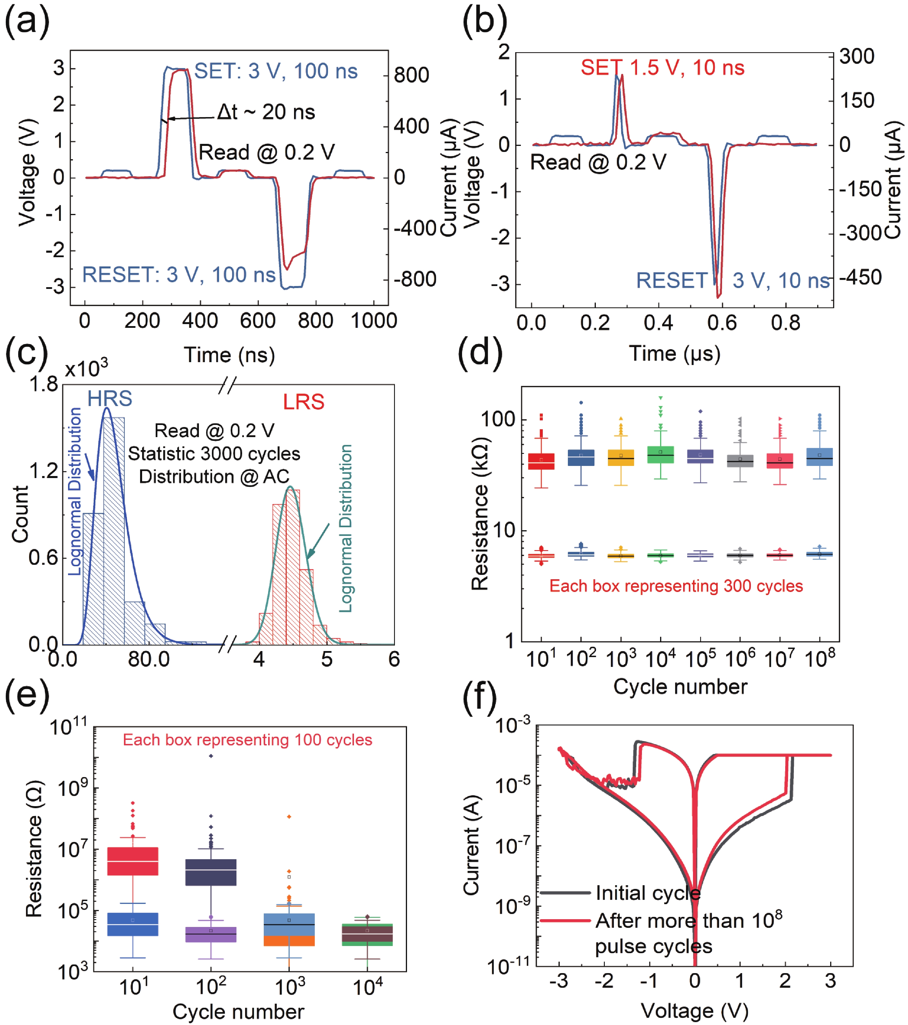
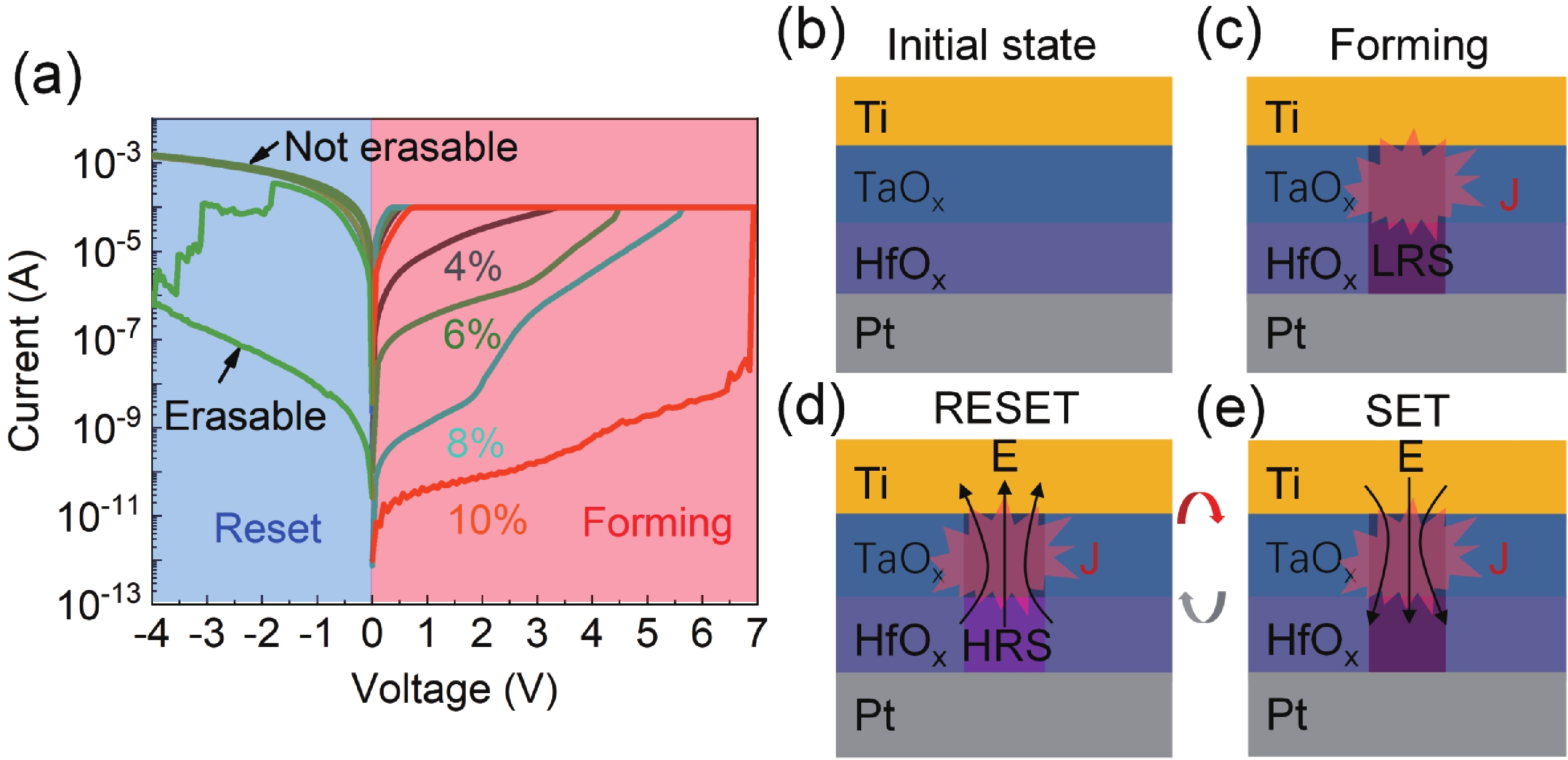
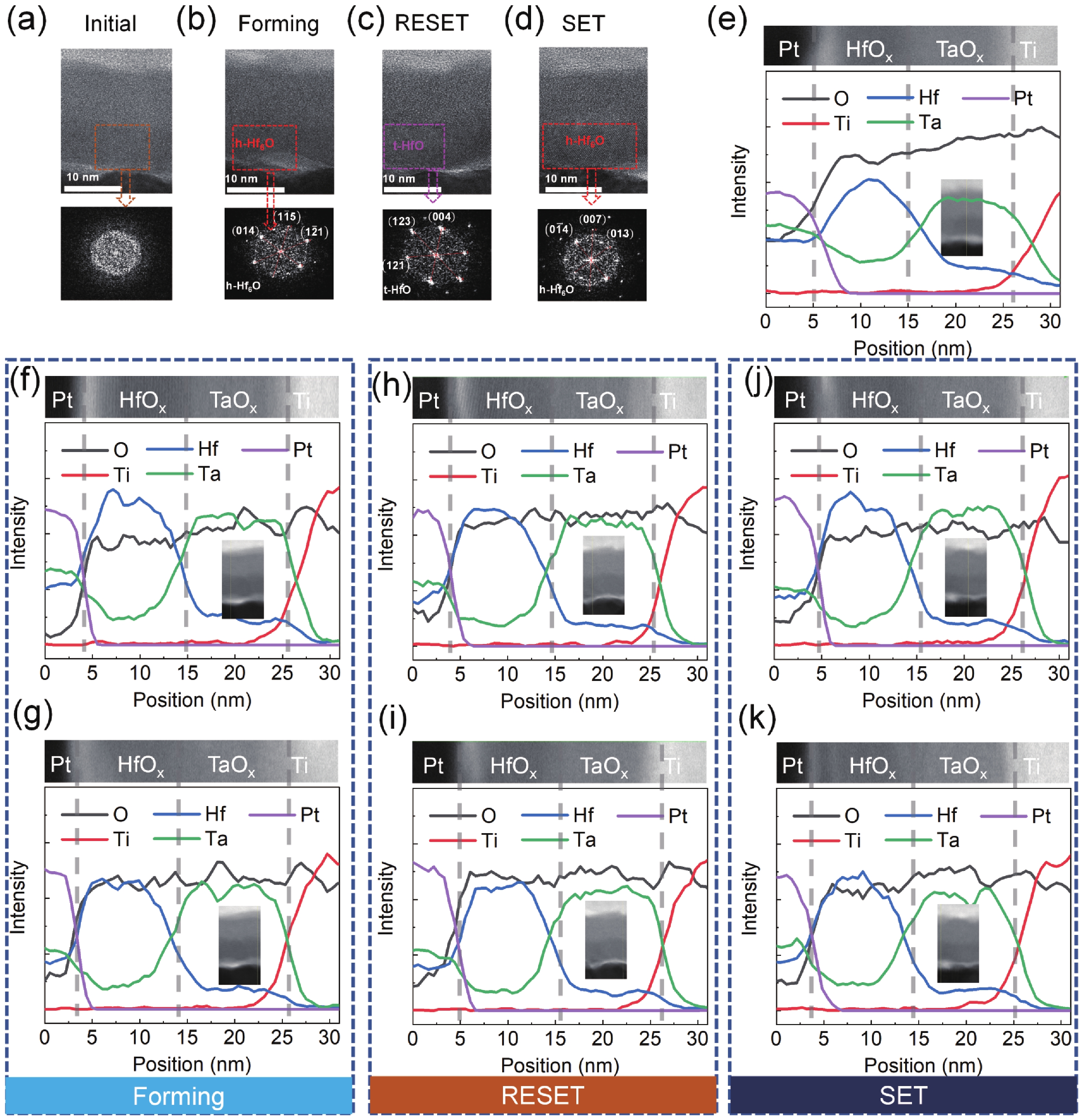
J. Semicond. > 2022, Volume 43 > Issue 5 > 054102

ARTICLES

Uniform, fast, and reliable CMOS compatible resistive switching memory

Yunxia Hao1, 2, Ying Zhang1, 2, Zuheng Wu3, , Xumeng Zhang4, Tuo Shi1, Yongzhou Wang1, Jiaxue Zhu1, 2, Rui Wang1, 2, Yan Wang1, 2 and Qi Liu1, 2, 4

+ Author Affiliations

 Corresponding author: Zuheng Wu, wuzuheng@ahu.edu.cn

DOI: 10.1088/1674-4926/43/5/054102

PDF

Turn off MathJax

Abstract: Resistive switching random access memory (RRAM) is considered as one of the potential candidates for next-generation memory. However, obtaining an RRAM device with comprehensively excellent performance, such as high retention and endurance, low variations, as well as CMOS compatibility, etc., is still an open question. In this work, we introduce an insert TaOx layer into HfOx-based RRAM to optimize the device performance. Attributing to robust filament formed in the TaOx layer by a forming operation, the local-field and thermal enhanced effect and interface modulation has been implemented simultaneously. Consequently, the RRAM device features large windows (> 103), fast switching speed (~ 10 ns), steady retention (> 72 h), high endurance (> 108 cycles), and excellent uniformity of both cycle-to-cycle and device-to-device. These results indicate that inserting the TaOx layer can significantly improve HfOx-based device performance, providing a constructive approach for the practical application of RRAM.

Key words: uniformityresistance switchingfield enhance layerthermal enhance layer and interface modulation

With the advent of the information age and the development of emerging technologies (such as IoT, 5G etc.), the amount of data generated by human society explodes, which brings the demand for high-density non-volatile memory (NVM) to store and process data[1-3]. Resistive switching random access memory (RRAM) devices, with the advantages of high switching speed[4, 5], high scalability (two-terminal structure)[6-8], low power consumption[9-11], and good compatibility with the back-end of the traditional CMOS process[12, 13], is considered as an excellent choice for high-density NVM. However, a RRAM device with comprehensively excellent performance, such as high retention and endurance, low variations, as well as CMOS compatibility, etc., is still an open question, which hinders the practical application of RRAM.

In prior works, researchers proposed various methods to improve the RRAM performance for practical applications. For example, localized filed enhancement effect by embedding of nanoscale materials in the electrode or resistive switching layer, etc., was adopted to improve the uniformity of RRAM devices[14, 15]. The thermal enhancement effect can accelerate the movement of oxygen vacancies/ions, decreasing the formation and rupture time of conductive filament (CF) and enabling fast switching performance[16]. Besides, inserting an additional thin film between the resistive switching layer and the electrode was used to improve the endurance of RRAM devices[17, 18]. Hence, synergying the field, thermal enhancement and interface modulation effect is a potential method to obtain the comprehensive excellent performance RRAM device. However, incorporating all of these factors to improve the RRAM device performance has rarely been reported.

TaOx with a low thermal conductance has been inserted into TaOx-based RRAM device as a thermal enhance and oxygen reservoir layer to modulate the RRAM performance in previous works[19, 20]. By forming a local CF in the TaOx layer to confine the electric field and current path, the local electric field and thermal enhancement effect can be achieved.

In this work, we inserted a TaOx layer into HfOx-based RRAM devices. Due to the localized field and thermal enhancement effect of the TaOx layer could be obtained by formation of confined CF after the forming process, the device performance could be modulated by all of the factors simultaneously and shows comprehensively excellent performance. The results indicated that the device could exhibit uniform switching, fast switching (~ 10 ns), steady retention (> 72 h) and high endurance (> 108 cycles) properties. These results provide a constructive approach for the practical application of RRAM.

The fabrication processes of Pt/Ti/TaOx/HfOx/Pt/Ti devices are as follow: Firstly, deposited the bottom electrode Pt/Ti (40/5 nm) by e-beam evaporation after the lithography process. The photoresist is removed by the lift-off process. Here, the former deposited Ti layer acts as an adhesive layer. Secondly, similar to the above-mentioned bottom electrode preparation process, deposited the dielectric layer TaOx/HfOx (10/10 nm) by magnetron sputtering. Thirdly, similarly, depositied the top electrode Pt/Ti (10/40 nm) by magnetron sputtering. Here, the deposited Pt layer acts as a capping layer.

Also, the fabrication processes of Pt/Ti/HfOx/Pt/Ti and Pt/Ti/TaOx/Pt/Ti devices were as same as the above-mentioned.

The SEM image of the device was obtained on Carl Zeiss Supra 55 Sapphire. The DC-mode and pulse mode characteristics of the device were measured at room temperature using an Agilent B1500A Semiconductor Characterization System. For all DC-mode and pulse mode measurements, the bias was applied to the top electrode and the bottom electrode was grounded.

In our work, the RRAM device is fabricated in a typical crossbar structure. The schematic structure of the device is shown in Fig. 1(a). And the insert shows the scanning electron microscope (SEM) result of the as-fabricated device. After the fabrication of the device, we characterized the device response property under DC voltage sweep. During the electrical measurement, the external voltage is applied on the top electrode (Ti), and the bottom electrode (Pt) is grounded. Fig. 1(b) shows the typical bipolar resistive switching behavior of Ti/TaOx/HfOx/Pt (red) and Ti/HfOx/Pt (gray) device. When the positive voltage sweep (0 V → 3 V → 0 V) is applied to the device, the device switches from a high-resistance state (HRS) to a low-resistance state (LRS), namely SET process. Here, a compliance current (Icc, 100 μA) was set to avoid the hard broken of the device. The negative voltage sweep (0 V → –3 V → 0 V) induces the device switching from LRS to HRS, namely, RESET process. Intuitively, the Ti/TaOx/HfOx/Pt device switching parameters (such as HRS, LRS, VSET, and VRESET) show excellent cycle-to-cycle uniformity. To clearly present the uniformity, we draw the cumulative distribution of these switching parameters in Ti/TaOx/HfOx/Pt device, as shown in Fig. 1(c). For the HRS/LRS distribution (left panel of Fig. 1(c)), we obtain that the LRS (HRS) average is 5 kΩ (17 MΩ) with a low standard deviation of 53 Ω (155 kΩ), indicating a low variation of ~1.06% (0.91%) in LRS (HRS). For operation voltages (right panel of Fig. 1(c)), the VSET (VRESET) averages are 2.0 V (–1.25 V) with a standard deviation of 0.16 V (0.15 V), indicating a variation of ~ 8% (12%). These results show that the Ti/TaOx/HfOx/Pt device could switch between the LRS and HRS with excellent uniform parameters. Additionally, in order to study the potential of the device as NVM in practical application, we investigate the resistance state retention ability by imposing a constant read voltage (0.2 V) on the device, as shown in Fig. 1(d). The both of HRS and LRS show no degradation under read voltage stress for more than 3.5 × 104 s. Furthermore, both of the HRS and LRS could still maintain after more than 72 h, as shown in the insert of Fig. 1(d). These results indicate that the Ti/TaOx/HfOx/Pt device shows excellent retention property for both resistance states.

Figure  1.  (Color online) Structure and switching performances of the Ti/TaOx/HfOx/Pt device. (a) Schematic of the Ti/ TaOx/HfOx/Pt device with a crossbar structure. The inset shows the SEM result of the as-fabricated device, the feature size of the fabricated device is 5 × 5 μm2. (b) The cyclic I–V curves of Ti/TaOx/HfOx/Pt (red) and Ti/HfOx/Pt (gray) device, which exhibits a typical bipolar resistive switching with uniform switching property. (c) The cumulative distribution of the resistance states (HRS and LRS) and operation voltages (VSET and VRESET) of Ti/TaOx/HfOx/Pt device. The HRS and LRS of Ti/TaOx/HfOx/Pt device is 17 ± 0.155 MΩ and 5 ± 0.053 kΩ, respectively. The VSET and VRESET of the device is 2.0 ± 0.16 V and –1.25 ± 0.15 V, respectively. (d) Retention characteristics of the HRS and LRS of Ti/TaOx/HfOx/Pt device for more than 3.5 × 10⁴ s. The insets show the measurement results after 24 and 72 h, respectively. The result shows the device with good retention property in both HRS and LRS.

Then, the response characteristics of the Ti/TaOx/HfOx/Pt device under pulse stimulus were investigated. Here, a strong pulse stimulus is essential for initialization the device for extreme fast pulse operation, called the initialization pulse. Fig. 2(a) shows the initialization pulse operation of the device. The pulses with identical width (100 ns) and different amplitudes for SET (3 V), RESET (–3 V), and Read (0.2 V) processes, respectively. In order to verify whether the switching of the device is successful, the read pulse (0.2 V) is set to before and after of each SET or RESET pulse. The result indicates that the device could be successfully programmed by this initialization pulse. In addition, as marked by the measured V–t (bule) and I–t (red) synchronous curves in Fig. 2(a), the SET speed of the device is about 20 ns under a 3 V/100 ns SET pulse.

Figure  2.  (Color online) The pulse mode switching characteristics of the Ti/TaOx/HfOx/Pt devices. (a) The device response characteristics of the initialization pulse operation. (b) The switching cycles of the device under extreme fast pulse stimulus. (c) The distribution of HRS/LRS under pulse mode switching. The statistical results show that this distribution conform to the lognormal distribution, indicating a uniform switching property of the device under pulse stimulus. (d) The Ti/TaOx/HfOx/Pt device exhibits reliable endurance for more than 108 cycles, each box in the figure representing 300 switching cycles. (e) The endurance property of the Ti/HfOx/Pt device, each box in the figure representing 100 switching cycles. (f) Comparison of I–V characteristics curves of the Ti/TaOx/HfOx/Pt device before (black line) and after (red line) the pulse measurement.

Furthermore, after the operation of the initialization pulse, consecutive extreme fast pulses were imposed on the device, as shown in Fig. 2(b). Here, a triangle pulse was used for SET and RESET process. Both the SET and RESET pulse is 10 ns rising edge and falling edge. Furthermore, due to both, the rising edge and falling edge of the triangle pulse is 10 ns, so that the full width at half maximum (FWHM) is 10 ns. Which means the device switching speed is about 10 ns. The pulse amplitude of SET and RESET process is 1.5 and –3 V, respectively. Read pulse with an amplitude of 0.2 V and width of 100 ns in order to read accurately. The results in Fig. 2(b) show that the devices can be tested under high frequency of MHz magnitude. The switching between HRS and LRS of the device can be clearly distinguished by the read response current. Where the former read current of SET pulse is lower than latter one and the former read current of RESET pulse is higher than the latter one. The device exhibits excellent reliability under this extreme fast pulse stimulation. What is more, the 3000 cycles HRS (left in Fig. 2(c)) and LRS (right in Fig. 2(c)) of the device under this extreme fast pulse stimulation were statistically analyzed, as shown in Fig. 2(c). The results exhibit that both of the HRS and LRS distribution conform to the lognormal distribution, indicating a uniform switching property of the device under pulse stimulus. Furthermore, the devices sustained more than 108 SET/RESET cycles under this extreme fast pulse stimulation, as shown in Fig. 2(d). Here, we extracted 300 cycles at each order. Each box in Fig. 2(d) respresents the resistance distribution of 300 cycles. However, the Ti/HfOx/Pt device endurance property is worse obviously than the Ti/TaOx/HfOx/Pt device, as shown in Fig. 2(e). It is worth noting that the Ti/HfOx/Pt device cannot be operated by the extreme fast pulse. The pulses with identical width (100 ns) and different amplitudes for SET (3 V), RESET (–3 V), and Read (0.2 V) processes, respectively, were used to characterize the Ti/HfOx/Pt device endurance property. Furthermore, in Figs. 2(d) and 2(e), the uniformity of the Ti/TaOx/HfOx/Pt device is obviously better than the Ti/HfOx/Pt device.

It is worth noting that, after the pulse measurements, the DC I–V sweep was imposed on the Ti/TaOx/HfOx/Pt device again to verify the performance of the device. As shown in Fig. 2(f), comparison of I–V characteristics of the device before (black line) and after (red line) the pulse measurements, indicating the resistance switching performance of the device is basically unchanged. This further confirms that the Ti/TaOx/HfOx/Pt device has excellent endurance. These results indicate that synergying the field, thermal enhancement and interface modulation effect is a method to obtain uniform, fast, and reliable device for practical NVM application.

The switching mechanisms of the device were analyzed. The HfOx-based RRAM device has been investigated widely[21-23]. However, the device with these attractive performances simultaneously has been rarely reported. Here, a TaOx layer was inserted in the HfOx-based RRAM device with the functions of confining E and J effects to optimize the performances of HfOx-based RRAM devices. It should be noted that, in previous works[19, 20], the thermal enhance property of TaOx was used to modulated the resistance switching performance of the HfOx based device. By inserting the TaOx thermal enhance layer, the HfOx-based device transition from abrupt switching to analog switching. However, in our work, the results are different from previous works[19, 20]. There is a difference in the TaOx layer between our work and previous works. In previous work, the TaOx layer is in LRS[19]. Whereas, in our work, the TaOx layer is in HRS state before the forming process. The intial HRS state TaOx obtained by modulating the oxygen/argon ratio during the spurting TaOx process. As indicated in Fig. 3(a), the intial state increases with the increment oxygen ratio. Furthermore, when oxygen ratio lower than 10%, the Ti/TaOx/Pt cannot be reset after the forming process. To form the robost CF in TaOx layer, the lower oxygen ratio would be preferable. Whereas the thermal conductivity increases with the decrement of oxygen ratio [24]. Hence, in this work, the oxygen ratio with 8% was used to deposite the TaOx insertion layer.

Figure  3.  (Color online) (a) The response property of Ti/TaOx/Pt device before and after the forming process. The initial resistance state modulated by the oxygen percentage during the spurting of the TaOx process. Schematic switching mechanisms of the Ti/TaOx/HfOx/Pt device. (b) Initial state, (c) forming process, (d) RESET process and (e) SET process.

The switching mechanisms of our device is summarized as the following. First, there are no CFs in the dielectric layers before the forming process, as shown in Fig. 3(b). Then the forming operation was performed on the device, inducing the formation of CFs in the dielectric layers, as illustrated in Fig. 3(c). The formed CFs confine the location of E and current through (namely, J) the device. The localized E and J would facilitate the rupture of the CFs during the RESET process, as illustrated in Fig. 3(d), inducing a uniform RESET property. Furthermore, due to the filament in the TaOx layer, this cannot be dissolved during the RESET process. Hence, when the set operation performed on the device, the confined E and J in TaOx layer would prompt the formation of the CFs in HfOx layer, as illustrated in Fig. 3(e), inducing a uniform SET property.

To further verify the switching mechians of the device, we investigated the cross-sectional high-resolution transmission electron microscopy (HRTEM) image and elements component profile and of devices under different operation conditions by energy dispersive spectrum (EDS), as shown in Fig. 4. As illustrated in Fig. 4(a), the HRTEM image shows that both of the HfOx and TaOx layer of the pristine device are in the amorphous state. In addition, the O/Hf and O/Ta ratio in the dielectric layer (HfOx/TaOx) of the pristine device is high, as shown in Fig. 4(e), and the device presents HRS. In the formed device, a crystalline region is in the HfOx layer and the TaOx layer is in amorphous state, as indicated in Fig. 4(b). The crystalline region is identified as h-Hf6O through fast Fourier transform (FFT)[25], which is a high conduction phase[25, 26]. The EDS line scan results indicate that the O/Hf and O/Ta ratio in the CF region reduced obviously after the forming operation, as shown in Fig. 4(f). Furthermore, the O/Hf and O/Ta ratio in the CF surrounding region is higher, as illustrated in Fig. 4(g). The results suggest that the oxygen vacancy CF formed in the device, after forming operation. The CF in the HfOx layer exhibits as Hf6O crystalline, which is similar to our previous work[25], whereas the CF in TaOx layer is amorphous, which is similar to previous work[27]. In the RESET device, the HRTEM image shows that there is a crystalline region in the HfOx layer and the TaOx layer is in the amorphous state, as shown in Fig. 4(c). Here, the crystalline region is identified as t-HfO through FFT[25]. The conductivity of t-HfO is lower than h-Hf6O[26], which attributed to the HRS. The EDS line scan results indicate that the O/Hf ratio in the CF region reduced obviously after the RESET operation, and the O/Ta ratio shows lower variation, as shown in Fig. 4(h). Furthermore, the O/Hf and O/Ta ratio in the CF surrounding region is higher, as illustrated in Fig. 4(i). These results indicate that the h-Hf6O CF in HfOx layer is reset into t-HfO by RESET operation and the oxygen vacancy CF in TaOx layer cannot be reset by RESET operation. Finally, in the SET device, the HRTEM images shows the similar results to Fig. 4(a) of the device under SET operation, as shown in Fig. 4(d). The O/Hf and O/Ta ratio in the CF region (Fig. 4(j)) and CF surrounding region (Fig. 4(k)) of the device under SET operation is similar to the forming operation. All the results further support the aforementioned analysis of the switching mechanism of the device.

Figure  4.  (Color online) The cross-sectional HRTEM image and the element component profile of the device under different operation conditions. The cross-sectional HRTEM image of (a) intial state, (b) forming, (c) RESET, (d) SET. (e) The element component profile of the pristine device. The (f) CF and (g) out of CF element component profile of the device under the forming operation. The (h) CF and (i) out of CF element component profile of the device under the RESET operation. The (j) CF and (k) out of the CF element component profile of the device under SET operation.

In conclusion, in this work, a TaOx layer was inserted in the HfOx-based RRAM device by taking advantage of all the field, thermal and interface modulation factors simultaneously to optimize the device performance. As a result, the Ti/TaOx/HfOx/Pt device shows excellent switching uniformity. In addition, the device also shows fast switching speed (~ 10 ns), steady retention (> 72 h) and reliable endurance (> 108 cycles). These desired performances implement in the same device simultaneously, making it a potential for practical NVM application.

This work was supported by the National Key R&D Program of China under Grant No. 2018YFA0701500, the National Natural Science Foundation of China under Grant Nos. 61825404, U20A20220, 61732020, and 61851402, the Strategic Priority Research Program of the Chinese Academy of Sciences under Grant No. XDB44000000 and the China Postdoctoral Science Foundation under Grant No. 2020M681167.


[1]
Shi T, Wang R, Wu Z H, et al. A review of resistive switching devices: Performance improvement, characterization, and applications. Small Struct, 2021, 2, 2170010 doi: 10.1002/sstr.202170010
[2]
Wang Z R, Wu H Q, Burr G W, et al. Resistive switching materials for information processing. Nat Rev Mater, 2020, 5, 173 doi: 10.1038/s41578-019-0159-3
[3]
Li X K, Zhang B T, Wang B W, et al. Low power and high uniformity of HfO x-based RRAM via tip-enhanced electric fields. Sci China Inf Sci, 2019, 62, 1 doi: 10.1007/s11432-019-9910-x
[4]
Zhao X L, Zhang X M, Shang D S, et al. Uniform, fast, and reliable LixSiOy-based resistive switching memory. IEEE Electron Device Lett, 2019, 40, 554 doi: 10.1109/LED.2019.2900261
[5]
Chen F T, Lee H Y, Chen Y S, et al. Resistance switching for RRAM applications. Sci China Inf Sci, 2011, 54, 1073 doi: 10.1007/s11432-011-4217-8
[6]
Han R Z, Huang P, Zhao Y D, et al. Efficient evaluation model including interconnect resistance effect for large scale RRAM crossbar array matrix computing. Sci China Inf Sci, 2018, 62, 1 doi: 10.1007/s11432-018-9555-8
[7]
Xia Q F, Yang J J. Memristive crossbar arrays for brain-inspired computing. Nat Mater, 2019, 18, 309 doi: 10.1038/s41563-019-0291-x
[8]
Wu Z, Lu J, Shi T, et al. A habituation sensory nervous system with memristors. Adv Mater, 2020, 32, e2004398 doi: 10.1002/adma.202004398
[9]
Wu Z H, Zhao X L, Yang Y, et al. Transformation of threshold volatile switching to quantum point contact originated nonvolatile switching in graphene interface controlled memory devices. Nanoscale Adv, 2019, 1, 3753 doi: 10.1039/C9NA00409B
[10]
Kim H J, Park T H, Yoon K J, et al. Fabrication of a Cu-cone-shaped cation source inserted conductive bridge random access memory and its improved switching reliability. Adv Funct Mater, 2019, 29, 1806278 doi: 10.1002/adfm.201806278
[11]
Lu Y F, Li Y, Li H Y, et al. Low-power artificial neurons based on Ag/TiN/HfAlO x/Pt threshold switching memristor for neuromorphic computing. IEEE Electron Device Lett, 2020, 41, 1245 doi: 10.1109/LED.2020.3006581
[12]
Sebastian A, le Gallo M, Khaddam-Aljameh R, et al. Memory devices and applications for in-memory computing. Nat Nanotechnol, 2020, 15, 529 doi: 10.1038/s41565-020-0655-z
[13]
Li H T, Wu T F, Mitra S, et al. Device-architecture co-design for hyperdimensional computing with 3d vertical resistive switching random access memory (3D VRRAM). 2017 International Symposium on VLSI Technology, Systems and Application, 2017, 1
[14]
Liu Q, Long S, Lv H, et al. Controllable growth of nanoscale conductive filaments in solid-electrolyte-based ReRAM by using a metal nanocrystal covered bottom electrode. ACS Nano, 2010, 4, 6162 doi: 10.1021/nn1017582
[15]
Li S S, Su Y K. Improvement of the performance in Cr-doped ZnO memory devices via control of oxygen defects. RSC Adv, 2019, 9, 2941 doi: 10.1039/C8RA10112D
[16]
Zhang Y Z, Huang P, Gao B, et al. Oxide-based filamentary RRAM for deep learning. J Phys D, 2021, 54, 083002 doi: 10.1088/1361-6463/abc5e7
[17]
Liu L, Xiong W, Liu Y X, et al. Designing high-performance storage in HfO2/BiFeO3 memristor for artificial synapse applications. Adv Electron Mater, 2020, 6, 1901012 doi: 10.1002/aelm.201901012
[18]
Park J H, Jeon D S, Kim T G. Improved uniformity in the switching characteristics of ZnO-based memristors using Ti sub-oxide layers. J Phys D, 2017, 50, 015104 doi: 10.1088/1361-6463/50/1/015104
[19]
Hao Z Q, Gao B, Xu M H, et al. Cryogenic HfO x-based resistive memory with a thermal enhancement capping layer. IEEE Electron Device Lett, 2021, 42, 1276 doi: 10.1109/LED.2021.3099725
[20]
Wu W, Wu H Q, Gao B, et al. Improving analog switching in HfO x-based resistive memory with a thermal enhanced layer. IEEE Electron Device Lett, 2017, 38, 1019 doi: 10.1109/LED.2017.2719161
[21]
Ryu H, Kim S. Pseudo-interface switching of a two-terminal TaO x/HfO2 synaptic device for neuromorphic applications. Nanomaterials, 2020, 10, 1550 doi: 10.3390/nano10081550
[22]
Yoon J H, Kwon D E, Kim Y, et al. The Current limit and self-rectification functionalities in the TiO2/HfO2 resistive switching material system. Nanoscale, 2017, 9, 11920 doi: 10.1039/C7NR02215H
[23]
Wedig A, Luebben M, Cho D Y, et al. Nanoscale cation motion in TaO x, HfO x and TiO x memristive systems. Nat Nanotech, 2016, 11, 67 doi: 10.1038/nnano.2015.221
[24]
Landon C D, Wilke R H T, Brumbach M T, et al. Erratum: “Thermal transport in tantalum oxide films for memristive applications. Appl Phys Lett, 2015, 107, 059902 doi: 10.1063/1.4928532
[25]
Zhang Y, Mao G Q, Zhao X L, et al. Evolution of the conductive filament system in HfO2-based memristors observed by direct atomic-scale imaging. Nat Commun, 2021, 12, 7232 doi: 10.1038/s41467-021-27575-z
[26]
Yin J, Zeng F, Wan Q, et al. Adaptive crystallite kinetics in homogenous bilayer oxide memristor for emulating diverse synaptic plasticity. Adv Funct Mater, 2018, 28, 1706927 doi: 10.1002/adfm.201706927
[27]
Miao F, Strachan J P, Yang J J, et al. Anatomy of a nanoscale conduction channel reveals the mechanism of a high-performance memristor. Adv Mater, 2011, 23, 5633 doi: 10.1002/adma.201103379
Fig. 1.  (Color online) Structure and switching performances of the Ti/TaOx/HfOx/Pt device. (a) Schematic of the Ti/ TaOx/HfOx/Pt device with a crossbar structure. The inset shows the SEM result of the as-fabricated device, the feature size of the fabricated device is 5 × 5 μm2. (b) The cyclic I–V curves of Ti/TaOx/HfOx/Pt (red) and Ti/HfOx/Pt (gray) device, which exhibits a typical bipolar resistive switching with uniform switching property. (c) The cumulative distribution of the resistance states (HRS and LRS) and operation voltages (VSET and VRESET) of Ti/TaOx/HfOx/Pt device. The HRS and LRS of Ti/TaOx/HfOx/Pt device is 17 ± 0.155 MΩ and 5 ± 0.053 kΩ, respectively. The VSET and VRESET of the device is 2.0 ± 0.16 V and –1.25 ± 0.15 V, respectively. (d) Retention characteristics of the HRS and LRS of Ti/TaOx/HfOx/Pt device for more than 3.5 × 10⁴ s. The insets show the measurement results after 24 and 72 h, respectively. The result shows the device with good retention property in both HRS and LRS.

Fig. 2.  (Color online) The pulse mode switching characteristics of the Ti/TaOx/HfOx/Pt devices. (a) The device response characteristics of the initialization pulse operation. (b) The switching cycles of the device under extreme fast pulse stimulus. (c) The distribution of HRS/LRS under pulse mode switching. The statistical results show that this distribution conform to the lognormal distribution, indicating a uniform switching property of the device under pulse stimulus. (d) The Ti/TaOx/HfOx/Pt device exhibits reliable endurance for more than 108 cycles, each box in the figure representing 300 switching cycles. (e) The endurance property of the Ti/HfOx/Pt device, each box in the figure representing 100 switching cycles. (f) Comparison of I–V characteristics curves of the Ti/TaOx/HfOx/Pt device before (black line) and after (red line) the pulse measurement.

Fig. 3.  (Color online) (a) The response property of Ti/TaOx/Pt device before and after the forming process. The initial resistance state modulated by the oxygen percentage during the spurting of the TaOx process. Schematic switching mechanisms of the Ti/TaOx/HfOx/Pt device. (b) Initial state, (c) forming process, (d) RESET process and (e) SET process.

Fig. 4.  (Color online) The cross-sectional HRTEM image and the element component profile of the device under different operation conditions. The cross-sectional HRTEM image of (a) intial state, (b) forming, (c) RESET, (d) SET. (e) The element component profile of the pristine device. The (f) CF and (g) out of CF element component profile of the device under the forming operation. The (h) CF and (i) out of CF element component profile of the device under the RESET operation. The (j) CF and (k) out of the CF element component profile of the device under SET operation.

[1]
Shi T, Wang R, Wu Z H, et al. A review of resistive switching devices: Performance improvement, characterization, and applications. Small Struct, 2021, 2, 2170010 doi: 10.1002/sstr.202170010
[2]
Wang Z R, Wu H Q, Burr G W, et al. Resistive switching materials for information processing. Nat Rev Mater, 2020, 5, 173 doi: 10.1038/s41578-019-0159-3
[3]
Li X K, Zhang B T, Wang B W, et al. Low power and high uniformity of HfO x-based RRAM via tip-enhanced electric fields. Sci China Inf Sci, 2019, 62, 1 doi: 10.1007/s11432-019-9910-x
[4]
Zhao X L, Zhang X M, Shang D S, et al. Uniform, fast, and reliable LixSiOy-based resistive switching memory. IEEE Electron Device Lett, 2019, 40, 554 doi: 10.1109/LED.2019.2900261
[5]
Chen F T, Lee H Y, Chen Y S, et al. Resistance switching for RRAM applications. Sci China Inf Sci, 2011, 54, 1073 doi: 10.1007/s11432-011-4217-8
[6]
Han R Z, Huang P, Zhao Y D, et al. Efficient evaluation model including interconnect resistance effect for large scale RRAM crossbar array matrix computing. Sci China Inf Sci, 2018, 62, 1 doi: 10.1007/s11432-018-9555-8
[7]
Xia Q F, Yang J J. Memristive crossbar arrays for brain-inspired computing. Nat Mater, 2019, 18, 309 doi: 10.1038/s41563-019-0291-x
[8]
Wu Z, Lu J, Shi T, et al. A habituation sensory nervous system with memristors. Adv Mater, 2020, 32, e2004398 doi: 10.1002/adma.202004398
[9]
Wu Z H, Zhao X L, Yang Y, et al. Transformation of threshold volatile switching to quantum point contact originated nonvolatile switching in graphene interface controlled memory devices. Nanoscale Adv, 2019, 1, 3753 doi: 10.1039/C9NA00409B
[10]
Kim H J, Park T H, Yoon K J, et al. Fabrication of a Cu-cone-shaped cation source inserted conductive bridge random access memory and its improved switching reliability. Adv Funct Mater, 2019, 29, 1806278 doi: 10.1002/adfm.201806278
[11]
Lu Y F, Li Y, Li H Y, et al. Low-power artificial neurons based on Ag/TiN/HfAlO x/Pt threshold switching memristor for neuromorphic computing. IEEE Electron Device Lett, 2020, 41, 1245 doi: 10.1109/LED.2020.3006581
[12]
Sebastian A, le Gallo M, Khaddam-Aljameh R, et al. Memory devices and applications for in-memory computing. Nat Nanotechnol, 2020, 15, 529 doi: 10.1038/s41565-020-0655-z
[13]
Li H T, Wu T F, Mitra S, et al. Device-architecture co-design for hyperdimensional computing with 3d vertical resistive switching random access memory (3D VRRAM). 2017 International Symposium on VLSI Technology, Systems and Application, 2017, 1
[14]
Liu Q, Long S, Lv H, et al. Controllable growth of nanoscale conductive filaments in solid-electrolyte-based ReRAM by using a metal nanocrystal covered bottom electrode. ACS Nano, 2010, 4, 6162 doi: 10.1021/nn1017582
[15]
Li S S, Su Y K. Improvement of the performance in Cr-doped ZnO memory devices via control of oxygen defects. RSC Adv, 2019, 9, 2941 doi: 10.1039/C8RA10112D
[16]
Zhang Y Z, Huang P, Gao B, et al. Oxide-based filamentary RRAM for deep learning. J Phys D, 2021, 54, 083002 doi: 10.1088/1361-6463/abc5e7
[17]
Liu L, Xiong W, Liu Y X, et al. Designing high-performance storage in HfO2/BiFeO3 memristor for artificial synapse applications. Adv Electron Mater, 2020, 6, 1901012 doi: 10.1002/aelm.201901012
[18]
Park J H, Jeon D S, Kim T G. Improved uniformity in the switching characteristics of ZnO-based memristors using Ti sub-oxide layers. J Phys D, 2017, 50, 015104 doi: 10.1088/1361-6463/50/1/015104
[19]
Hao Z Q, Gao B, Xu M H, et al. Cryogenic HfO x-based resistive memory with a thermal enhancement capping layer. IEEE Electron Device Lett, 2021, 42, 1276 doi: 10.1109/LED.2021.3099725
[20]
Wu W, Wu H Q, Gao B, et al. Improving analog switching in HfO x-based resistive memory with a thermal enhanced layer. IEEE Electron Device Lett, 2017, 38, 1019 doi: 10.1109/LED.2017.2719161
[21]
Ryu H, Kim S. Pseudo-interface switching of a two-terminal TaO x/HfO2 synaptic device for neuromorphic applications. Nanomaterials, 2020, 10, 1550 doi: 10.3390/nano10081550
[22]
Yoon J H, Kwon D E, Kim Y, et al. The Current limit and self-rectification functionalities in the TiO2/HfO2 resistive switching material system. Nanoscale, 2017, 9, 11920 doi: 10.1039/C7NR02215H
[23]
Wedig A, Luebben M, Cho D Y, et al. Nanoscale cation motion in TaO x, HfO x and TiO x memristive systems. Nat Nanotech, 2016, 11, 67 doi: 10.1038/nnano.2015.221
[24]
Landon C D, Wilke R H T, Brumbach M T, et al. Erratum: “Thermal transport in tantalum oxide films for memristive applications. Appl Phys Lett, 2015, 107, 059902 doi: 10.1063/1.4928532
[25]
Zhang Y, Mao G Q, Zhao X L, et al. Evolution of the conductive filament system in HfO2-based memristors observed by direct atomic-scale imaging. Nat Commun, 2021, 12, 7232 doi: 10.1038/s41467-021-27575-z
[26]
Yin J, Zeng F, Wan Q, et al. Adaptive crystallite kinetics in homogenous bilayer oxide memristor for emulating diverse synaptic plasticity. Adv Funct Mater, 2018, 28, 1706927 doi: 10.1002/adfm.201706927
[27]
Miao F, Strachan J P, Yang J J, et al. Anatomy of a nanoscale conduction channel reveals the mechanism of a high-performance memristor. Adv Mater, 2011, 23, 5633 doi: 10.1002/adma.201103379
1

Perovskite plasmonic lasers capable of mode modulation

Jingbi You

Journal of Semiconductors, 2019, 40(7): 070203. doi: 10.1088/1674-4926/40/7/070203

2

Improved interfacial properties of GaAs MOS capacitor with NH3-plasma-treated ZnON as interfacial passivation layer

Jingkang Gong, Jingping Xu, Lu Liu, Hanhan Lu, Xiaoyu Liu, et al.

Journal of Semiconductors, 2017, 38(9): 094004. doi: 10.1088/1674-4926/38/9/094004

3

Layer-number dependent high-frequency vibration modes in few-layer transition metal dichalcogenides induced by interlayer couplings

Qing-Hai Tan, Xin Zhang, Xiang-Dong Luo, Jun Zhang, Ping-Heng Tan, et al.

Journal of Semiconductors, 2017, 38(3): 031006. doi: 10.1088/1674-4926/38/3/031006

4

Study of the effect of switching speed of the a-SiC/c-Si (p)-based, thyristor-like, ultra-high-speed switches, using two-dimensional simulation techniques

Evangelos I. Dimitriadis, Nikolaos Georgoulas

Journal of Semiconductors, 2017, 38(5): 054001. doi: 10.1088/1674-4926/38/5/054001

5

Comparison between Pt/TiO2/Pt and Pt/TaOX/TaOY/Pt based bipolar resistive switching devices

Patrick W. C. Ho, Firas Odai Hatem, Haider Abbas F. Almurib, T. Nandha Kumar

Journal of Semiconductors, 2016, 37(6): 064001. doi: 10.1088/1674-4926/37/6/064001

6

Influences of ICP etching damages on the electronic properties of metal field plate 4H-SiC Schottky diodes

Hui Wang, Yingxi Niu, Fei Yang, Yong Cai, Zehong Zhang, et al.

Journal of Semiconductors, 2015, 36(10): 104006. doi: 10.1088/1674-4926/36/10/104006

7

An InGaAs graded buffer layer in solar cells

Xiaosheng Qu, Hongyin Bao, Hanieh. S. Nikjalal, Liling Xiong, Hongxin Zhen, et al.

Journal of Semiconductors, 2014, 35(1): 014011. doi: 10.1088/1674-4926/35/1/014011

8

MOS Capacitance-Voltage Characteristics: V. Methods to Enhance the Trapping Capacitance

Jie Binbin, Sah Chihtang

Journal of Semiconductors, 2012, 33(2): 021001. doi: 10.1088/1674-4926/33/2/021001

9

Optical and electrical properties of porous silicon layer formed on the textured surface by electrochemical etching

Ou Weiying, Zhao Lei, Diao Hongwei, Zhang Jun, Wang Wenjing, et al.

Journal of Semiconductors, 2011, 32(5): 056002. doi: 10.1088/1674-4926/32/5/056002

10

MOS structure fabrication by thermal oxidation of multilayer metal thin films

Mohammad Orvatinia, Atefeh Chahkoutahi

Journal of Semiconductors, 2011, 32(3): 036001. doi: 10.1088/1674-4926/32/3/036001

11

A dual VCDL DLL based gate driver for zero-voltage-switching DC-DC converter

Tian Xin, Liu Xiangxin, Li Wenhong

Journal of Semiconductors, 2010, 31(7): 075012. doi: 10.1088/1674-4926/31/7/075012

12

High contrast ratio, high uniformity multiple quantum well spatial light modulators

Huang Yuyang, Liu H C, Wasilewski Z, Buchanan M, Laframboise S R, et al.

Journal of Semiconductors, 2010, 31(3): 034007. doi: 10.1088/1674-4926/31/3/034007

13

Effects of the reciprocating parameters of the carrier on material removal rate and non-uniformity in CMP

Wang Cailing, Kang Renke, Jin Zhuji, Guo Dongming

Journal of Semiconductors, 2010, 31(12): 126001. doi: 10.1088/1674-4926/31/12/126001

14

An A/D interface based on Σ Δ modulator for thermal vacuum sensor ASICs

Li Jinfeng, Tang Zhen'an

Journal of Semiconductors, 2010, 31(7): 075008. doi: 10.1088/1674-4926/31/7/075008

15

Conductivity modulation enhanced lateral IGBT with SiO2 shielded layer anode by SIMOX technology on SOI substrate

Chen Wensuo, Zhang Bo, Li Zhaoji, Fang Jian, Guan Xu, et al.

Journal of Semiconductors, 2010, 31(6): 064004. doi: 10.1088/1674-4926/31/6/064004

16

Boron-doped silicon film as a recombination layer in the tunnel junction of a tandem solar cell

Shi Mingji, Wang Zhanguo, Liu Shiyong, Peng Wenbo, Xiao Haibo, et al.

Journal of Semiconductors, 2009, 30(6): 063001. doi: 10.1088/1674-4926/30/6/063001

17

Improving Carbon Nanotube Field Emission Display Luminescence Uniformity by Introducing a Reactive Current Limiting Layer

Li Xin, He Yongning, Liu Weihua, Zhu Changchun

Journal of Semiconductors, 2008, 29(3): 574-577.

18

Uniformity Investigation in 3C-SiC Epitaxial Layers Grown on Si Substrates by Horizontal Hot-Wall CVD

Li Jiaye, Zhao Yongmei, Liu Xingfang, Sun Guosheng, Luo Muchang, et al.

Chinese Journal of Semiconductors , 2007, 28(1): 1-4.

19

Fabrication and Numerical Simulation of a Micromachined Contact Cantilever RF-MEMS Switch

Sun Jianhai, Cui Dafu, Xiao Jiang

Chinese Journal of Semiconductors , 2006, 27(2): 309-312.

20

Synthesis and Characterization of SiCOF/a-C∶F Double-Layer Films with Low Dielectric Constant for Copper Interconnects

Zhang Wei, Zhu Lian, Sun Qingqing, Lu Hongliang, Ding Shijin, et al.

Chinese Journal of Semiconductors , 2006, 27(3): 429-433.

1. Tian, Q., Xun, K., Li, Z. et al. Optoelectronic memristor based on a-C:Te film for muti-mode reservoir computing. Journal of Semiconductors, 2025, 46(2): 022407. doi:10.1088/1674-4926/24100008
2. Mir, K.H., Garg, T. Effect of annealing conditions on resistive switching in hafnium oxide-based MIM devices for low-power RRAM. Physica Scripta, 2024, 99(12): 125941. doi:10.1088/1402-4896/ad8d19
3. Mir, K.H., Gupta, Y., Gupta, R. et al. Tailoring resistive switching in pulsed laser ablated forming-free hafnia thin films based RRAM devices via digital SET and gradual RESET. Applied Physics A: Materials Science and Processing, 2024, 130(11): 844. doi:10.1007/s00339-024-08002-8
4. Fadeev, A.V., Rudenko, K.V. Evolution of the Current–Voltage Characteristic of a Bipolar Memristor. Russian Microelectronics, 2024, 53(4): 297-302. doi:10.1134/S1063739724600432
5. Kim, S., Hong, K., Kim, H. et al. Overshoot-Suppressed Memristor Array with AlN Oxygen Barrier for Low-Power Operation in the Intelligent Neuromorphic Systems. Advanced Intelligent Systems, 2024, 6(8): 2300797. doi:10.1002/aisy.202300797
6. Wu, Z., Hu, Y., Feng, Z. et al. A tantalum oxide based memristive neuron device for anomaly detection application. Applied Physics Letters, 2024, 124(23): 233505. doi:10.1063/5.0212850
7. Wu, Z., Yu, R., Hu, Y. et al. A multifunctional and reconfigurable memristive neuron circuit. Electronics Letters, 2024, 60(11): e13245. doi:10.1049/ell2.13245
8. Fadeev, A.V., Rudenko, K.V. Filament-based memristor switching model. Microelectronic Engineering, 2024. doi:10.1016/j.mee.2024.112179
9. Feng, Y., Chen, B., Tang, M. et al. Near-threshold-voltage operation in flash-based high-precision computing-in-memory to implement Poisson image editing. Science China Information Sciences, 2023, 66(12): 222402. doi:10.1007/s11432-022-3743-x
  • Search

    Advanced Search >>

    GET CITATION

    Yunxia Hao, Ying Zhang, Zuheng Wu, Xumeng Zhang, Tuo Shi, Yongzhou Wang, Jiaxue Zhu, Rui Wang, Yan Wang, Qi Liu. Uniform, fast, and reliable CMOS compatible resistive switching memory[J]. Journal of Semiconductors, 2022, 43(5): 054102. doi: 10.1088/1674-4926/43/5/054102
    Y X Hao, Y Zhang, Z H Wu, X M Zhang, T Shi, Y Z Wang, J X Zhu, R Wang, Y Wang, Q Liu. Uniform, fast, and reliable CMOS compatible resistive switching memory[J]. J. Semicond, 2022, 43(5): 054102. doi: 10.1088/1674-4926/43/5/054102
    shu

    Export: BibTex EndNote

    Article Metrics

    Article views: 1739 Times PDF downloads: 112 Times Cited by: 9 Times

    History

    Received: 30 November 2021 Revised: 30 December 2021 Online: Uncorrected proof: 15 February 2022Accepted Manuscript: 15 February 2022Published: 01 May 2022

    Catalog

      Email This Article

      User name:
      Email:*请输入正确邮箱
      Code:*验证码错误
      Yunxia Hao, Ying Zhang, Zuheng Wu, Xumeng Zhang, Tuo Shi, Yongzhou Wang, Jiaxue Zhu, Rui Wang, Yan Wang, Qi Liu. Uniform, fast, and reliable CMOS compatible resistive switching memory[J]. Journal of Semiconductors, 2022, 43(5): 054102. doi: 10.1088/1674-4926/43/5/054102 ****Y X Hao, Y Zhang, Z H Wu, X M Zhang, T Shi, Y Z Wang, J X Zhu, R Wang, Y Wang, Q Liu. Uniform, fast, and reliable CMOS compatible resistive switching memory[J]. J. Semicond, 2022, 43(5): 054102. doi: 10.1088/1674-4926/43/5/054102
      Citation:
      Yunxia Hao, Ying Zhang, Zuheng Wu, Xumeng Zhang, Tuo Shi, Yongzhou Wang, Jiaxue Zhu, Rui Wang, Yan Wang, Qi Liu. Uniform, fast, and reliable CMOS compatible resistive switching memory[J]. Journal of Semiconductors, 2022, 43(5): 054102. doi: 10.1088/1674-4926/43/5/054102 ****
      Y X Hao, Y Zhang, Z H Wu, X M Zhang, T Shi, Y Z Wang, J X Zhu, R Wang, Y Wang, Q Liu. Uniform, fast, and reliable CMOS compatible resistive switching memory[J]. J. Semicond, 2022, 43(5): 054102. doi: 10.1088/1674-4926/43/5/054102

      Uniform, fast, and reliable CMOS compatible resistive switching memory

      DOI: 10.1088/1674-4926/43/5/054102
      More Information
      • Yunxia Hao:is currently pursuing a master's degree in Institute of Microelectronics, Chinese Academy of Sciences, Beijing. Her research focuses on resistive switching memory
      • Zuheng Wu:received his PhD degree from the Institute of Microelectronics, Chinese Academy of Sciences, Beijing, in 2021. His research focuses on memristors and neuromorphic computing
      • Corresponding author: wuzuheng@ahu.edu.cn
      • Received Date: 2021-11-30
      • Accepted Date: 2022-02-10
      • Revised Date: 2021-12-30
      • Available Online: 2022-04-19

      Catalog

        /

        DownLoad:  Full-Size Img  PowerPoint
        Return
        Return