| [1] |
Zhou Y, Chen J, Bakr O M, et al. Metal halide perovskites for X-ray imaging scintillators and detectors. ACS Energy Lett, 2021, 6, 739 doi: 10.1021/acsenergylett.0c02430 |
| [2] |
Wu H, Ge Y, Niu G, et al. Metal halide perovskites for X-ray detection and imaging. Matter, 2021, 4, 144 doi: 10.1016/j.matt.2020.11.015 |
| [3] |
Wei H, Huang J. Halide lead perovskites for ionizing radiation detection. Nat Commun, 2019, 10, 1066 doi: 10.1038/s41467-019-08981-w |
| [4] |
Olivo A, Chana D, Speller R. A preliminary investigation of the potential of phase contrast X-ray imaging in the field of homeland security. J Phys D, 2008, 41, 225503 doi: 10.1088/0022-3727/41/22/225503 |
| [5] |
Guerra M, Manso M, Longelin S, et al. Performance of three different Si X-ray detectors for portable XRF spectrometers in cultural heritage applications. J Instrum, 2012, 7, C10004 doi: 10.1088/1748-0221/7/10/C10004 |
| [6] |
Kasap S. X-ray sensitivity of photoconductors: application to stabilized α-Se. J Phys D, 2000, 33, 2853 doi: 10.1088/0022-3727/33/21/326 |
| [7] |
Street R, Ready S, Van Schuylenbergh K, et al. Comparison of PbI 2 and HgI 2 for direct detection active matrix X-ray image sensors. J Appl Phys, 2002, 91, 3345 doi: 10.1063/1.1436298 |
| [8] |
Del Sordo S, Abbene L, Caroli E, et al. Progress in the development of CdTe and CdZnTe semiconductor radiation detectors for astrophysical and medical applications. Sensors, 2009, 9, 3491 doi: 10.3390/s90503491 |
| [9] |
Su Y, Ma W, Yang Y M. Perovskite semiconductors for direct X-ray detection and imaging. J Semicond, 2020, 41, 051204 doi: 10.1088/1674-4926/41/5/051204 |
| [10] |
Yakunin S, Dirin D N, Shynkarenko Y, et al. Detection of gamma photons using solution-grown single crystals of hybrid lead halide perovskites. Nat Photonics, 2016, 10, 585 doi: 10.1038/nphoton.2016.139 |
| [11] |
Huang J, Yuan Y, Shao Y, et al. Understanding the physical properties of hybrid perovskites for photovoltaic applications. Nat Rev Mater, 2017, 2, 17042 doi: 10.1038/natrevmats.2017.42 |
| [12] |
Wei H, Fang Y, Mulligan P, et al. Sensitive X-ray detectors made of methylammonium lead tribromide perovskite single crystals. Nat Photonics, 2016, 10, 333 doi: 10.1038/nphoton.2016.41 |
| [13] |
Zhou F, Li Z, Lan W, et al. Halide perovskite, a potential scintillator for X-ray detection. Small Methods, 2020, 4, 2000506 doi: 10.1002/smtd.202000506 |
| [14] |
Li C, Ma Y, Xiao Y, et al. Advances in perovskite photodetectors. InfoMat, 2020, 2, 1247 doi: 10.1002/inf2.12141 |
| [15] |
Song Y, Li L, Bi W, et al. Atomistic surface passivation of CH 3NH 3PbI 3 perovskite single crystals for highly sensitive coplanar-structure X-ray detectors. Research, 2020, 2020, 5958243 doi: 10.34133/2020/5958243 |
| [16] |
Zheng X, Zhao W, Wang P, et al. Ultrasensitive and stable X-ray detection using zero-dimensional lead-free perovskites. J Energy Chem, 2020, 49, 299 doi: 10.1016/j.jechem.2020.02.049 |
| [17] |
Pan W, Yang B, Niu G, et al. Hot-pressed CsPbBr 3 quasi-monocrystalline film for sensitive direct X-ray detection. Adv Mater, 2019, 31, 1904405 doi: 10.1002/adma.201904405 |
| [18] |
Thirimanne H, Jayawardena K, Parnell A, et al. High sensitivity organic inorganic hybrid X-ray detectors with direct transduction and broadband response. Nat Commun, 2018, 9, 2926 doi: 10.1038/s41467-018-05301-6 |
| [19] |
Demchyshyn S, Verdi M, Basirico L, et al. Designing ultraflexible perovskite X-ray detectors through interface engineering. Adv Sci, 2020, 7, 2002586 doi: 10.1002/advs.202002586 |
| [20] |
Liu J, Shabbir B, Wang C, et al. Flexible, printable soft-X-ray detectors based on all-inorganic perovskite quantum dots. Adv Mater, 2019, 31, 1901644 doi: 10.1002/adma.201901644 |
| [21] |
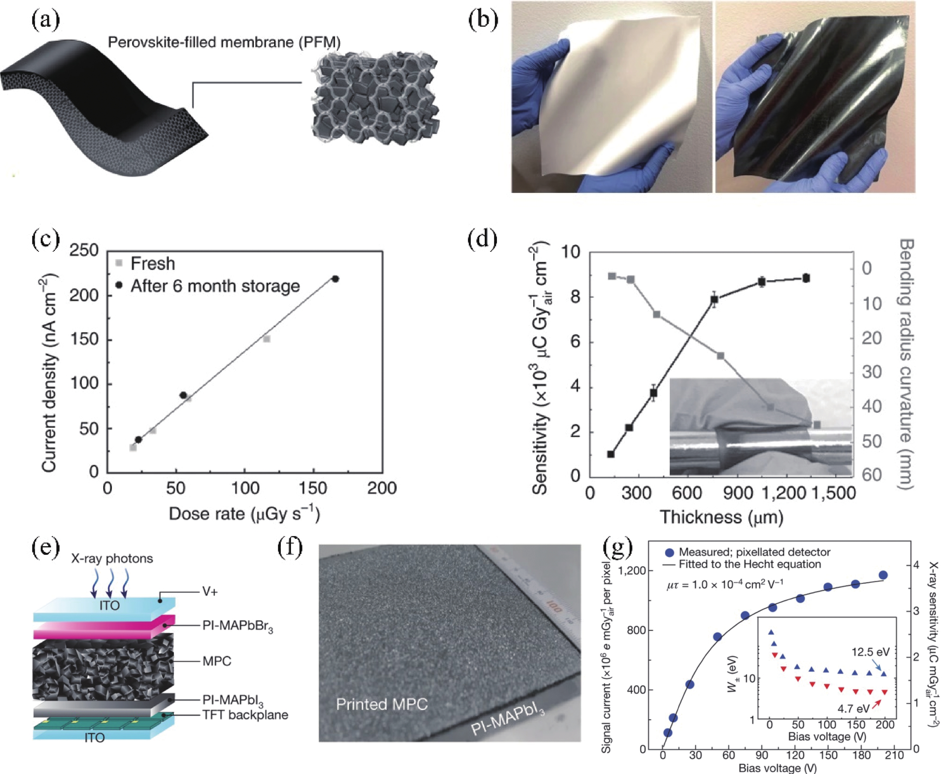
Zhao J, Zhao L, Deng Y, et al. Perovskite-filled membranes for flexible and large-area direct-conversion X-ray detector arrays. Nat Photonics, 2020, 14, 612 doi: 10.1038/s41566-020-0678-x |
| [22] |
Kim Y C, Kim K H, Son D Y, et al. Printable organometallic perovskite enables large-area, low-dose X-ray imaging. Nature, 2017, 550, 87 doi: 10.1038/nature24032 |
| [23] |
He X, Xia M, Wu H, et al. Quasi-2D perovskite thick film for X-ray detection with low detection limit. Adv Funct Mater, 2021, 32, 2109458 doi: 10.1002/adfm.202109458 |
| [24] |
Datta A, Zhong Z, Motakef S. A new generation of direct X-ray detectors for medical and synchrotron imaging applications. Sci Rep, 2020, 10, 20097 doi: 10.1038/s41598-020-76647-5 |
| [25] |
Brenner D J, Elliston C D, Hall E J, et al. Estimated risks of radiation-induced fatal cancer from pediatric CT. Am J Roentgenol, 2001, 176, 289 doi: 10.2214/ajr.176.2.1760289 |
| [26] |
Yang B, Pan W, Wu H, et al. Heteroepitaxial passivation of Cs 2AgBiBr 6 wafers with suppressed ionic migration for X-ray imaging. Nat Commun, 2019, 10, 1989 doi: 10.1038/s41467-018-07882-8 |
| [27] |
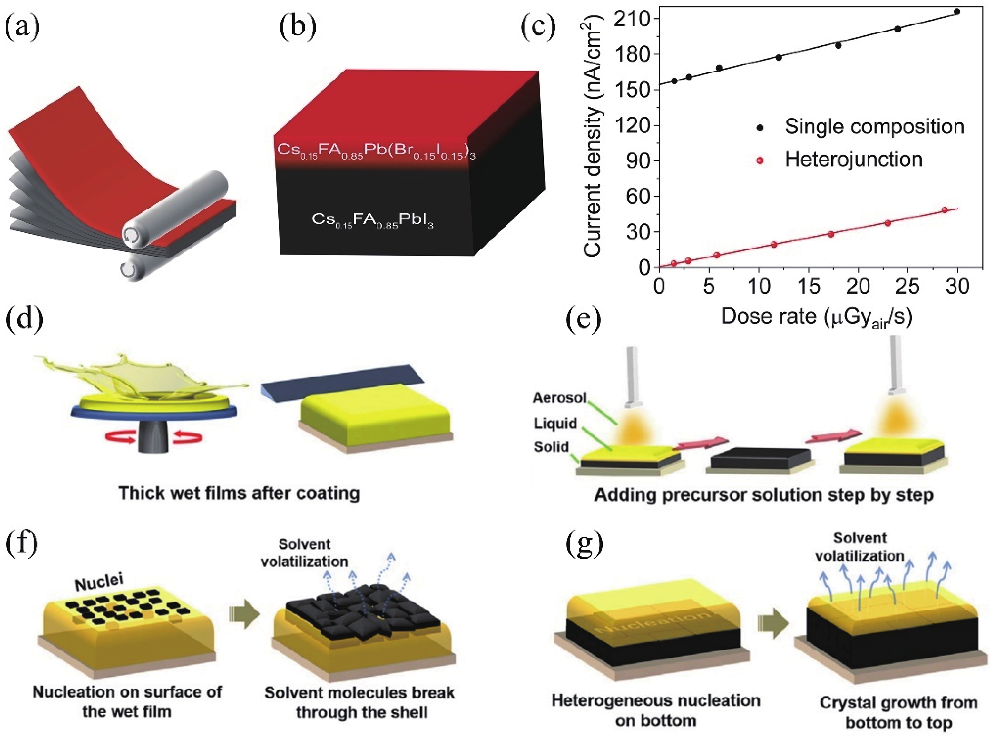
Zhou Y, Zhao L, Ni Z, et al. Heterojunction structures for reduced noise in large-area and sensitive perovskite X-ray detectors. Sci Adv, 2021, 7, eabg6716 doi: 10.1126/sciadv.abg6716 |
| [28] |
Gill H S, Elshahat B, Kokil A, et al. Flexible perovskite based X-ray detectors for dose monitoring in medical imaging applications. Phys Med, 2018, 5, 20 doi: 10.1016/j.phmed.2018.04.001 |
| [29] |
Chen S, Xiao X, Chen B, et al. Crystallization in one-step solution deposition of perovskite films: Upward or downward. Sci Adv, 2021, 7, eabb2412 doi: 10.1126/sciadv.abb2412 |
| [30] |
Qian W, Xu X, Wang J, et al. An aerosol-liquid-solid process for the general synthesis of halide perovskite thick films for direct-conversion X-ray detectors. Matter, 2021, 4, 942 doi: 10.1016/j.matt.2021.01.020 |


 DownLoad: