| [1] |
Pearton S J, Yang J C, Cary P H IV, et al. A review of Ga 2O 3 materials, processing, and devices. Appl Phys Rev, 2018, 5, 011301 doi: 10.1063/1.5006941 |
| [2] |
Stepanov S I, Nikolaev V I, Bougrov V E, et al. Gallium oxide: properties and applications− a review. Rev Adv Mater Sci, 2016, 44, 63
|
| [3] |
Butenko P N, Guzilova L I, Chikiryaka A V, et al. Impact on the subsurface layers of the single-crystal β-Ga 2O 3 wafers induced by a mechanical wear. Mater Sci Semicond Process, 2022, 143, 106520 doi: 10.1016/j.mssp.2022.106520 |
| [4] |
Gao S, Wu Y Q, Kang R K, et al. Nanogrinding induced surface and deformation mechanism of single crystal β-Ga 2O 3. Mater Sci Semicond Process, 2018, 79, 165 doi: 10.1016/j.mssp.2017.12.017 |
| [5] |
Huang C J, Mu W X, Zhou H, et al. Effect of OH − on chemical mechanical polishing of β-Ga 2O 3 (100) substrate using an alkaline slurry. RSC Adv, 2018, 8, 6544 doi: 10.1039/C7RA11570A |
| [6] |
Oshima T, Hashiguchi A, Moribayashi T, et al. Electrical properties of Schottky barrier diodes fabricated on (001) β-Ga 2O 3 substrates with crystal defects. Jpn J Appl Phys, 2017, 56, 086501 doi: 10.7567/JJAP.56.086501 |
| [7] |
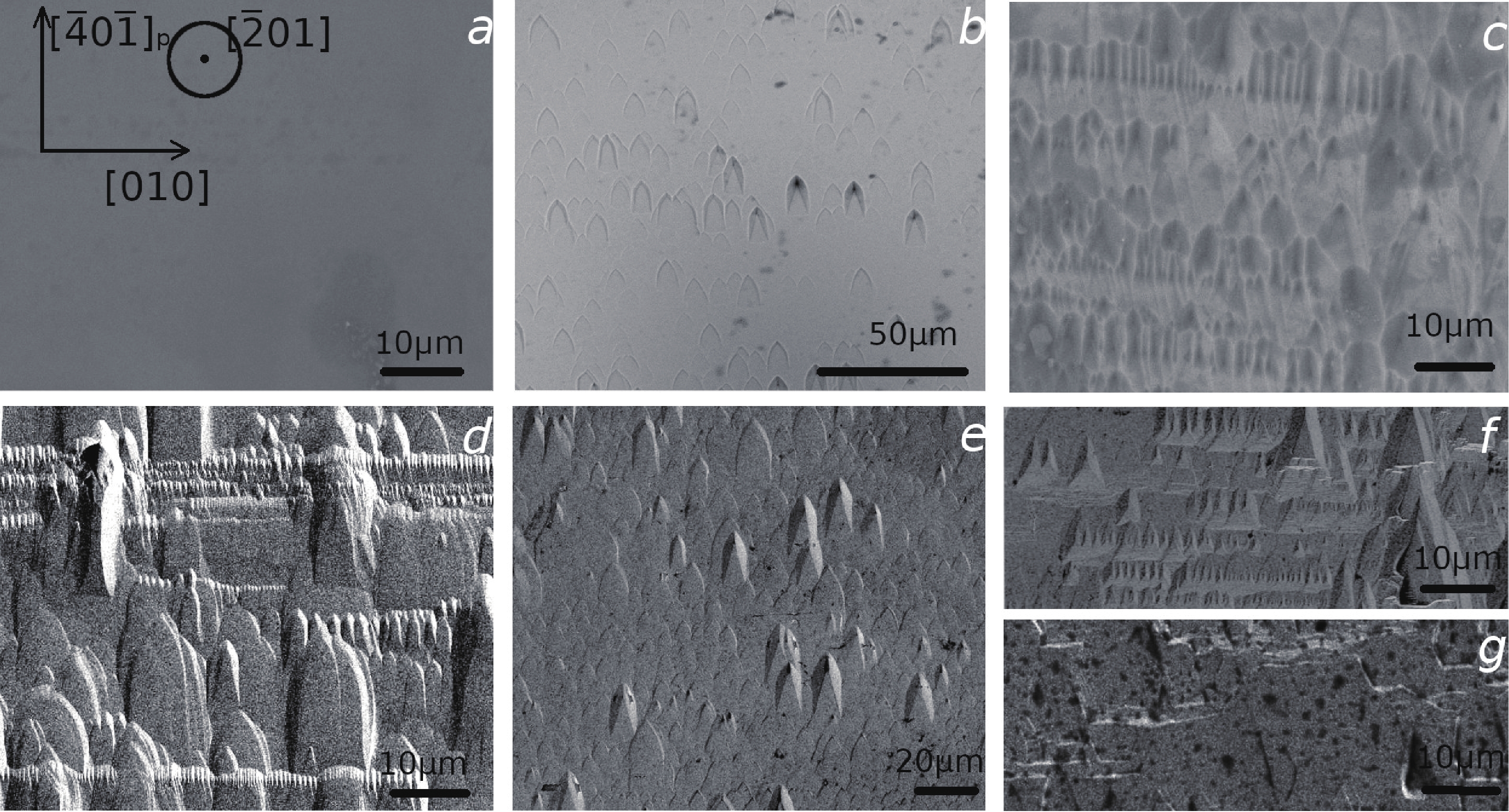
Kasu M, Oshima T, Hanada K, et al. Crystal defects observed by the etch-pit method and their effects on Schottky-barrier-diode characteristics on (-201) β-Ga 2O 3. Jpn J Appl Phys, 2017, 56, 091101 doi: 10.7567/JJAP.56.091101 |
| [8] |
Williamson G K, Hall W H. X-ray line broadening from filed aluminium and wolfram. Acta Metall, 1953, 1, 22 doi: 10.1016/0001-6160(53)90006-6 |
| [9] |
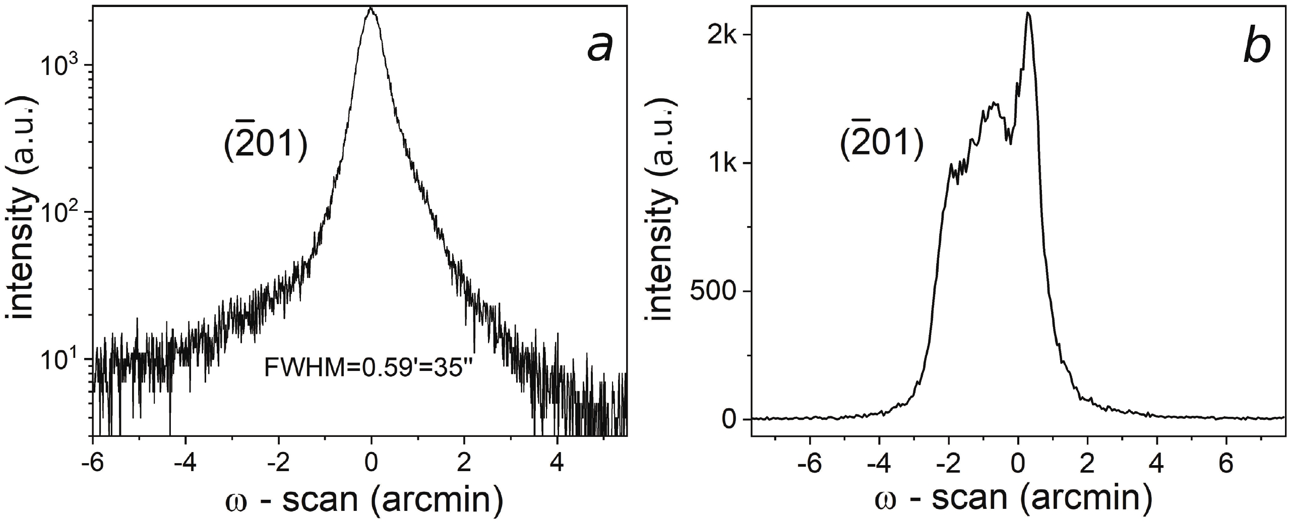
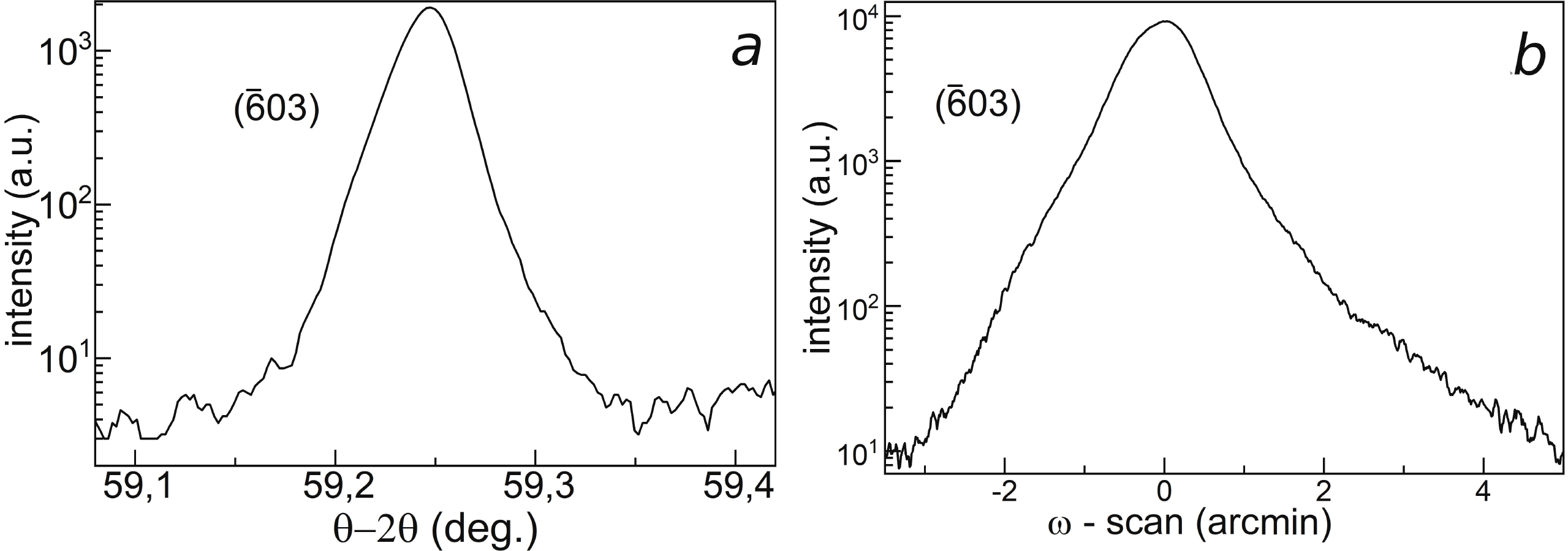
Boiko M E, Sharkov M D, Boiko A M, et al. Investigation of the atomic, crystal, and domain structures of materials based on X-ray diffraction and absorption data: A review. Tech Phys, 2015, 60, 1575 doi: 10.1134/S1063784215110067 |
| [10] |
Yao Y Z, Sugawara Y, Ishikawa Y. Observation of dislocations in β-Ga 2O 3 single-crystal substrates by synchrotron X-ray topography, chemical etching, and transmission electron microscopy. Jpn J Appl Phys, 2020, 59, 045502 doi: 10.35848/1347-4065/ab7dda |
| [11] |
Yao Y Z, Sugawara Y, Sato K, et al. Etch pit formation on β-Ga 2O 3 by molten KOH+NaOH and hot H 3PO 4 and their correlation with dislocations. J Alloys Compd, 2022, 910, 164788 doi: 10.1016/j.jallcom.2022.164788 |
| [12] |
Lu D Z, Jiang Q T, Ma X M, et al. Defect-related etch pits on crystals and their utilization. Crystals, 2022, 12, 1549 doi: 10.3390/cryst12111549 |
| [13] |
Mazzolini P, Vogt P, Schewski R, et al. Faceting and metal-exchange catalysis in (010) β-Ga 2O 3 thin films homoepitaxially grown by plasma-assisted molecular beam epitaxy. APL Mater, 2019, 7, 022511 doi: 10.1063/1.5054386 |
| [14] |
Huang H C, Ren Z J, Chan C, et al. Wet etch, dry etch, and MacEtch of β-Ga 2O 3: A review of characteristics and mechanism. J Mater Res, 2021, 36, 4756 doi: 10.1557/s43578-021-00413-0 |
| [15] |
Ogawa K, Ogawa N, Kosaka R, et al. AFM observation of etch-pit shapes on β-Ga 2O 3 (001) surface formed by molten alkali etching. Mater Sci Forum, 2020, 1004, 512 doi: 10.4028/www.scientific.net/MSF.1004.512 |
| [16] |
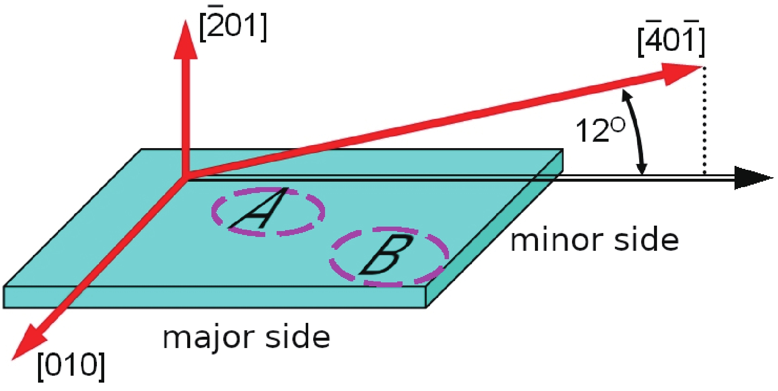
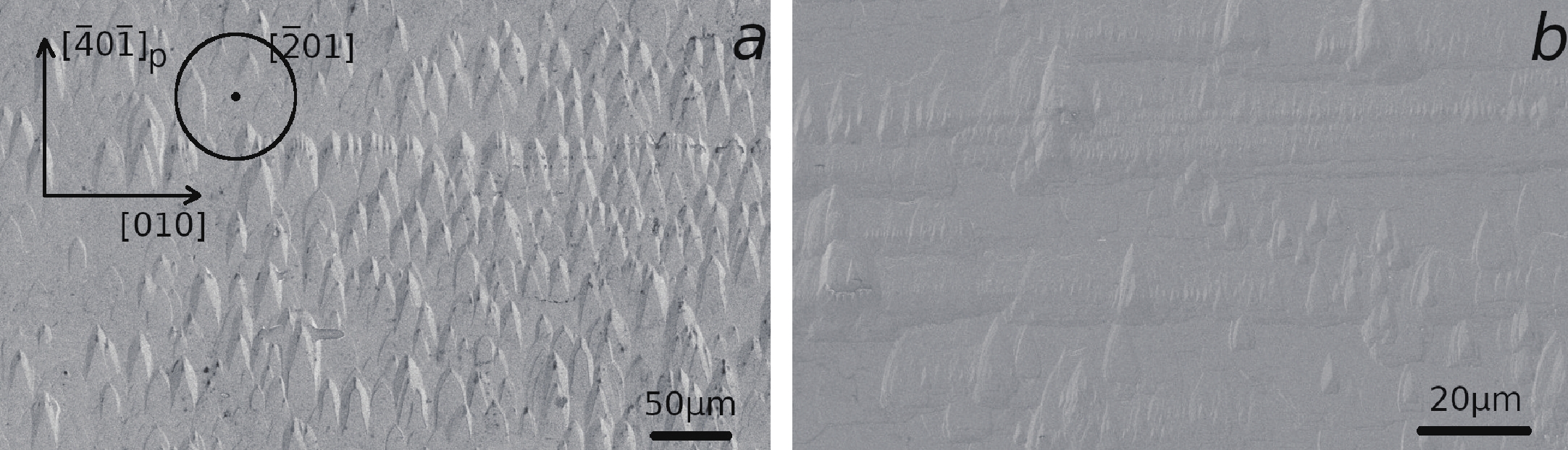
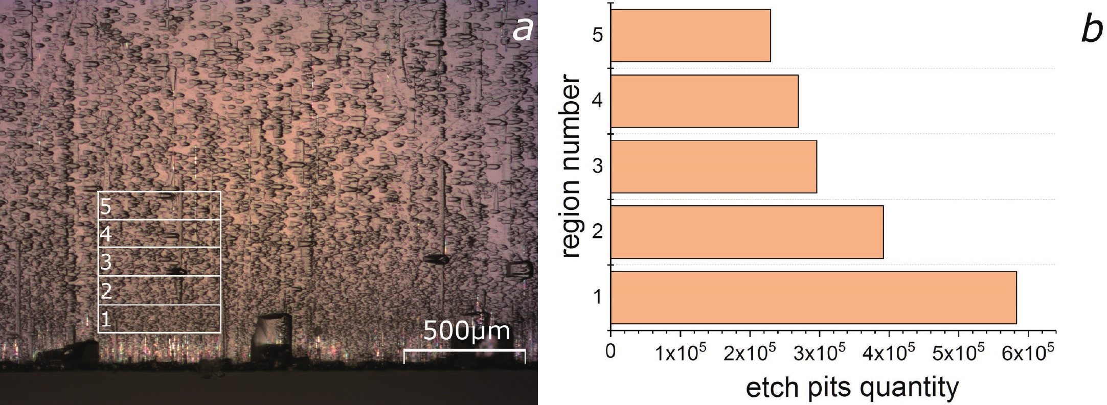
Zarichny A A, Butenko P N, Boiko M E, et al. The analysis of the etch pits parameters in the ( $ \bar{2}01 $) plane of the β-Ga 2O 3 substrate crystals. Materials Physics and Mechanics, 2023, 51(3), 174 doi: 10.18149/MPM.5132023_6 |
| [17] |
Ueda O, Ikenaga N, Koshi K, et al. Structural evaluation of defects in β-Ga 2O 3 single crystals grown by edge-defined film-fed growth process. Jpn J Appl Phys, 2016, 55, 1202BD doi: 10.7567/JJAP.55.1202BD |


 DownLoad:


 Pavel Butenko received his PhD from Peter the Great St. Petersburg Polytechnic University, St. Petersburg, Russia in 2006. He has held various positions at universities in Russia, Germany and China. He is currently a senior researcher in Physics of Shaped Crystals Laboratory, Solid State Physics Department at Ioffe Institute, Russian Academy of Sciences, St. Petersburg, Russia and Laboratory of Ultrawide Bandgap Semiconductors, Department of Semiconductor Electronics and Semiconductor Physics at MISIS University, Moscow, Russia. His research interests include: metal-oxide semiconductors; liquid-phase crystal growth and epitaxy; obtaining free-standing substrates by exfoliation; structure characterization; structure defects
 Michael Boiko received his PhD in Ioffe Institute, Russian Academy of Sciences, Saint-Petersburg, Russia in 1993. He is currently associated professor with Ioffe Institute. At present his research interest include XRD, SAXS, EXAFS of crystal structure and super structure of domains in semiconductors and dielectrics
 Mikhail Sharkov received his PhD in Ioffe Institute, Russian Academy of Sciences, St. Petersburg, Russia in 2009. Now he is working in the same institute at a position of senior researcher. His regions of interest are X-ray-based methods of materials studying, semiconductor heterostructures and XRD data modeling
 Aleksei Almaev received his PhD in the area of Physical and Mathematical Sciences from National Research Tomsk State University, Tomsk, Russia, in 2018. He is currently a Head of the Laboratory of Metal Oxide Semiconductors at Research and Development Center for Advanced Technologies in Microelectronics of the National Research Tomsk State University. His current research interests are metal oxide semiconductors, related devices and functional coatings
 Aleksnder Kitsay received his Master’s degree in engineering in 1976 from St. Petersburg State Institute of Technology, St. Petersburg, Russia. He worked as a researcher at the V. G. Khlopin Radium Institute, St. Petersburg, Russia. He is currently a researcher in Physics of Shaped Crystals Laboratory, Solid State Physics Department at Ioffe Institute, Russian Academy of Sciences. His current research interests include semiconductor crystal growth by flux method
 Vladimir Krymov received his PhD in Ioffe Institute, Russian Academy of Sciences, St. Petersburg, Russia in 1978. No he is working as a senior researcher at the Ioffe Institute, Russian Academy of Sciences. His research interests include the growth and characterization of sapphire and gallium oxide bulk crystals
 Anton Zarichny got his bachelor's degree in 2017 and his master's degree in 2023 from Peter the Great St. Petersburg Polytechnic University, St. Petersburg, Russia. Now he is a PhD student in Physics of Shaped Crystals Laboratory at Ioffe Institute, Russian Academy of Sciences. His research focuses on the characterization of ultrawide bandgap metal-oxide semiconductors
 Vladimir Nikolaev received a PhD in solid state physics from the Ioffe Institute, St. Petersburg, Russia in 1989. In 1990, Dr. Nikolaev was awarded the Prize of the Physical Society of the Ioffe Institute for the discovery of the electro-plastic effect in ferroelectric crystals. Currently, Dr. Nikolaev is the Head of the Physics of Shaped Crystals laboratory at the Ioffe Institute. He is also the founder and CEO of Perfect Crystals LLC. He has published more than 300 scientific articles in peer-reviewed journals, has six granted patents and several chapters in books on electronics and smart materials. He is on the editorial board of the Technical Physics journal


