


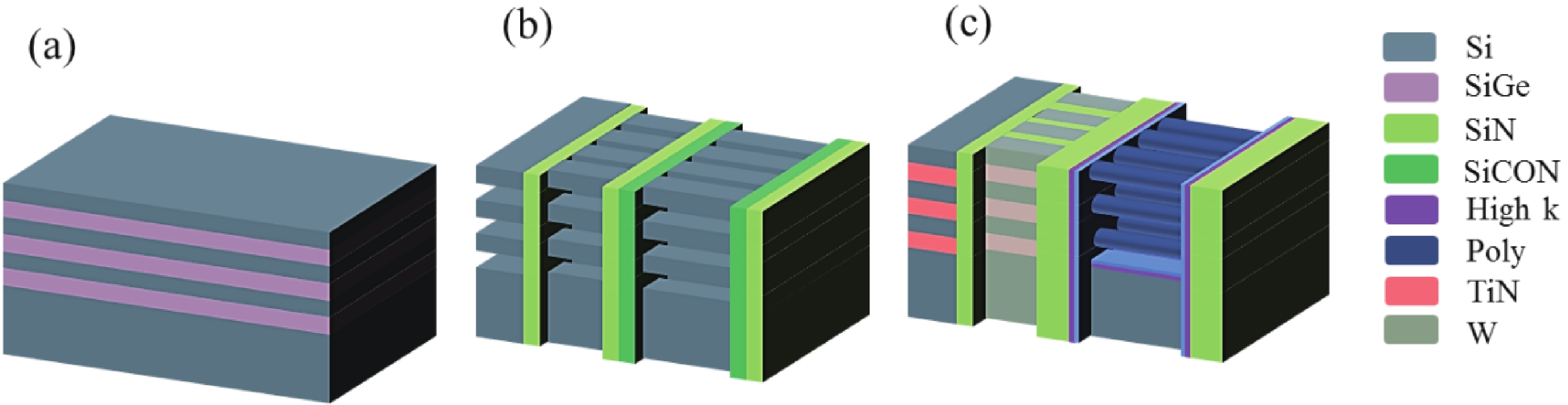
Fig. 1.
(Color online) (a) Si/SiGe epitaxy; (b) SiGe full release; (c) high-k and top electrode deposition.
ARTICLES
Zhenzhen Kong1, 4, Hongxiao Lin3, 4, Hailing Wang2, Yanpeng Song2, Junjie Li1, Xiaomeng Liu2, Anyan Du1, Yuanhao Miao1, 3, Yiwen Zhang1, 4, Yuhui Ren1, 4, Chen Li1, 4, Jiahan Yu1, 4, Jinbiao Liu1, 4, Jingxiong Liu1, 4, Qinzhu Zhang1, Jianfeng Gao1, Huihui Li2, Xiangsheng Wang2, Junfeng Li1, Henry H. Radamson3, Chao Zhao2, Tianchun Ye1, 4 and Guilei Wang2, 5,
Corresponding author: Guilei Wang, Guilei.Wang@bjsamt.org.cn
Abstract: Fifteen periods of Si/Si0.7Ge0.3 multilayers (MLs) with various SiGe thicknesses are grown on a 200 mm Si substrate using reduced pressure chemical vapor deposition (RPCVD). Several methods were utilized to characterize and analyze the ML structures. The high resolution transmission electron microscopy (HRTEM) results show that the ML structure with 20 nm Si0.7Ge0.3 features the best crystal quality and no defects are observed. Stacked Si0.7Ge0.3 ML structures etched by three different methods were carried out and compared, and the results show that they have different selectivities and morphologies. In this work, the fabrication process influences on Si/SiGe MLs are studied and there are no significant effects on the Si layers, which are the channels in lateral gate all around field effect transistor (L-GAAFET) devices. For vertically-stacked dynamic random access memory (VS-DRAM), it is necessary to consider the dislocation caused by strain accumulation and stress release after the number of stacked layers exceeds the critical thickness. These results pave the way for the manufacture of high-performance multivertical-stacked Si nanowires, nanosheet L-GAAFETs, and DRAM devices.
Keywords: RPCVD, epitaxy, SiGe/Si multilayers, L-GAAFETs, VS-DRAM
| [1] |
Radamson H H, Zhu H L, Wu Z H, et al. State of the art and future perspectives in advanced CMOS technology. Nanomaterials (Basel), 2020, 10, 1555 doi: 10.3390/nano10081555
|
| [2] |
Radamson H H, Simeon E. CMOS past, present and future. Amsterdam: Elsevier, 2018, 105
|
| [3] |
Loubet N, Kal S, Alix C, et al. A novel dry selective etch of SiGe for the enablement of high performance logic stacked gate-all-around NanoSheet devices. 2019 IEEE International Electron Devices Meeting (IEDM), 2020, 11.4. 1 doi: 10.1109/IEDM19573.2019.8993615
|
| [4] |
Radamson H H, Zhang Y B, He X B, et al. The challenges of advanced CMOS process from 2D to 3D. Appl Sci, 2017, 7, 1047 doi: 10.3390/app7101047
|
| [5] |
Radamson H H, He X B, Zhang Q Z, et al. Miniaturization of cmos. Micromachines, 2019, 10, 293 doi: 10.3390/mi10050293
|
| [6] |
Radamson H H, Joelsson K B, Ni W X, et al. Characterization of highly boron-doped Si, Si1− xGe x and Ge layers by high-resolution transmission electron microscopy. J Cryst Growth, 1995, 157, 80 doi: 10.1016/0022-0248(95)00375-4
|
| [7] |
Wang G L, Luo J, Qin C L, et al. Integration of highly strained SiGe in source and drain with HK and MG for 22 nm bulk PMOS transistors. Nanoscale Res Lett, 2017, 12, 123 doi: 10.1186/s11671-017-1908-0
|
| [8] |
Singh N, Buddharaju K D, Manhas S K, et al. Si, SiGe nanowire devices by top–down technology and their applications. IEEE Trans Electron Devices, 2008, 55, 3107 doi: 10.1109/TED.2008.2005154
|
| [9] |
Barraud S, Previtali B, Lapras V, et al. Top-down fabrication and electrical characterization of Si and SiGe nanowires for advanced CMOS technologies. Semicond Sci Technol, 2019, 34, 074001 doi: 10.1088/1361-6641/ab1e5b
|
| [10] |
Radamson H H, Kolahdouz M. Selective epitaxy growth of Si1− xGe x layers for MOSFETs and FinFETs. J Mater Sci: Mater Electron, 2015, 26, 4584 doi: 10.1007/s10854-015-3123-z
|
| [11] |
Chu C L, Wu K, Luo G L, et al. Stacked Ge-nanosheet GAAFETs fabricated by Ge/Si multilayer epitaxy. IEEE Electron Device Lett, 2018, 39, 1133 doi: 10.1109/LED.2018.2850366
|
| [12] |
Veloso A, Paraschiv V, Vecchio E, et al. (invited) challenges on surface conditioning in 3D device architectures: Triple-gate FinFETs, gate-all-around lateral and vertical nanowire FETs. ECS Trans, 2017, 80, 3 doi: 10.1149/08002.0003ecst
|
| [13] |
Neisser M. International roadmap for devices and systems lithography roadmap. J Micro/nanopatterning Mater Metrol, 2021, 20, 44601 doi: 10.1117/1.JMM.20.4.044601
|
| [14] |
Ha D, Kim H S. Prospective innovation of DRAM, flash, and logic technologies for digital transformation (DX) era. 2022 IEEE Symposium on VLSI Technology and Circuits (VLSI Technology and Circuits), 2022, 417 doi: 10.1109/VLSITechnologyandCir46769.2022.9830465
|
| [15] |
Huang M, Si S F, He Z, et al. A 3D stackable 1T1C DRAM: Architecture, process integration and circuit simulation. 2023 IEEE International Memory Workshop (IMW), 2023, 1 doi: 10.1109/IMW56887.2023.10145931
|
| [16] |
Han J W, Park S H, Jeong M Y, et al. Ongoing evolution of DRAM scaling via third dimension-vertically stacked DRAM . 2023 IEEE Symposium on VLSI Technology and Circuits (VLSI Technology and Circuits), 2023, 1 doi: 10.23919/VLSITechnologyandCir57934.2023.10185290
|
| [17] |
Rachidi S, Campo A, Loup V, et al. Isotropic dry etching of Si selectively to Si0.7Ge0.3 for CMOS sub-10 nm applications. J Vac Sci Technol A Vac Surf Films, 2020, 38, 033002 doi: 10.1116/1.5143118
|
| [18] |
Huynh-Bao T, Sakhare S, Yakimets D, et al. A comprehensive benchmark and optimization of 5-nm lateral and vertical GAA 6T-SRAMs. IEEE Trans Electron Devices, 2016, 63, 643 doi: 10.1109/TED.2015.2504729
|
| [19] |
Liu Y C, Tu C T, Tsai C E, et al. First highly stacked Ge0.95Si0.05 nGAAFETs with record ION = 110 μA (4100 μA/μm) at VOV=VDS=0.5V and high Gm, max = 340 μS (13000 μS/μm) at VDS=0.5V by wet etching. 2021 Symposium on VLSI Technology, 2021, 1
|
| [20] |
Li J J, Wang W W, Li Y L, et al. Study of selective isotropic etching Si1− xGe x in process of nanowire transistors. J Mater Sci:Mater Electron, 2020, 31, 134 doi: 10.1007/s10854-019-02269-x
|
| [21] |
Lee S, Jeong J, Yoon J S, et al. Sensitivity of inner spacer thickness variations for sub-3-nm node silicon nanosheet field-effect transistors. Nanomaterials, 2022, 12, 3349 doi: 10.3390/nano12193349
|
| [22] |
Reboh S, Coquand R, Barraud S, et al. Strain, stress, and mechanical relaxation in fin-patterned Si/SiGe multilayers for sub-7 nm nanosheet gate-all-around device technology. Appl Phys Lett, 2018, 112, 051901 doi: 10.1063/1.5010997
|
| [23] |
Tuppen C G, Gibbings C J, Hockly M. Mismatch dislocation nucleation and propagation in Si/Si1− xGe x heterostructures. MRS Proc, 1988, 130, 185 doi: 10.1557/PROC-130-185
|
| [24] |
Barbisan L, Marzegalli A, Montalenti F. Atomic-scale insights on the formation of ordered arrays of edge dislocations in Ge/Si(001) films via molecular dynamics simulations. Sci Rep, 2022, 12, 3235 doi: 10.1038/s41598-022-07206-3
|
| [25] |
Orlowski M, Ndoye C, Liu T, et al. (invited) Si, SiGe, Ge, and III-V semiconductor nanomembranes and nanowires enabled by SiGe epitaxy. ECS Trans, 2010, 33, 777 doi: 10.1149/1.3487608
|
| [26] |
Borel S, Arvet C, Bilde J, et al. Isotropic etching of SiGe alloys with high selectivity to similar materials. Microelectron Eng, 2004, 73/74, 301 doi: 10.1016/S0167-9317(04)00115-7
|
| [27] |
Caubet V, Beylier C, Borel S, et al. Mechanisms of isotropic and selective etching between SiGe and Si. J Vac Sci Technol B Microelectron Nanometer Struct Process Meas Phenom, 2006, 24, 2748 doi: 10.1116/1.2393244
|
| [28] |
Zhao Y, Iwase T, Satake M, et al. Formation mechanism of rounded SiGe-etch front in isotropic SiGe plasma etching for gate-all-around FETs. IEEE J Electron Devices Soc, 2021, 9, 1112 doi: 10.1109/JEDS.2021.3130916
|
| [29] |
Chang W Y, Luo G L, Huang Y S, et al. SiGe and Si gate-all-around FET fabricated by selective etching the same epitaxial layers. 2022 6th IEEE Electron Devices Technology & Manufacturing Conference (EDTM), 2022, 21 doi: 10.1109/EDTM53872.2022.9797991
|
| [30] |
Wostyn K, Sebaai F, Rip J, et al. (invited) selective etch of Si and SiGe for gate all-around device architecture. ECS Trans, 2015, 69, 147 doi: 10.1149/06908.0147ecst
|
| [31] |
Choi Y, Jang H, Byun D S, et al. Selective chemical wet etching of Si1- xGe x versus Si in single-layer and multi-layer with HNO3/HF mixtures. Thin Solid Films, 2020, 709, 138230 doi: 10.1016/j.tsf.2020.138230
|
| [32] |
Kim S, Kim M, Ryu D, et al. Investigation of electrical characteristic behavior induced by channel-release process in stacked nanosheet gate-all-around MOSFETs. IEEE Trans Electron Devices, 2020, 67, 2648 doi: 10.1109/TED.2020.2989416
|
| [33] |
Zhuge J, Wang R S, Huang R, et al. Experimental investigation and design optimization guidelines of characteristic variability in silicon nanowire CMOS technology. 2009 IEEE International Electron Devices Meeting (IEDM), 2010, 1 doi: 10.1109/IEDM.2009.5424421
|
| [34] |
Sous S A, Hildmann B O, Kaysser W A. Characterization of dislocation densities in germanium and silicon single crystals by high resolution X-ray diffraction. Phys Stat Sol (a), 1997, 159, 343 doi: 10.1002/1521-396X(199702)159:2<343::AID-PSSA343>3.0.CO;2-#
|
| [35] |
Radamson H H, Moeen M, Abedin A, et al. Sensitivity of signal-to-noise ratio to the layer profile and crystal quality of SiGe/Si multilayers. ECS J Solid State Sci Technol, 2016, 5, P3196 doi: 10.1149/2.0261604jss
|
| [36] |
Hartmann J M, Papon A M, Barnes J P, et al. Growth kinetics of SiGe/Si superlattices on bulk and silicon-on-insulator substrates for multi-channel devices. J Cryst Growth, 2009, 311, 3152 doi: 10.1016/j.jcrysgro.2009.03.027
|
| [37] |
Radamson H H, Hållstedt J. Application of high-resolution X-ray diffraction for detecting defects in SiGe(C) materials. J Phys: Condens Matter, 2005, 17, S2315 doi: 10.1088/0953-8984/17/22/020
|
| [38] |
Destefanis V, Hartmann J M, Hopstaken M, et al. Low-thermal surface preparation, HCl etch and Si/SiGe selective epitaxy on (1 1 0) silicon surfaces. Semicond Sci Technol, 2008, 23, 105018 doi: 10.1088/0268-1242/23/10/105018
|
| [39] |
Loubet N, Kormann T, Chabanne G, et al. Selective etching of Si1− xGe x versus Si with gaseous HCl for the formation of advanced CMOS devices. Thin Solid Films, 2008, 517, 93 doi: 10.1016/j.tsf.2008.08.081
|
| [40] |
Mertens H, Ritzenthaler R, Hikavyy A, et al. Gate-all-around MOSFETs based on vertically stacked horizontal Si nanowires in a replacement metal gate process on bulk Si substrates. 2016 IEEE Symposium on VLSI Technology, 2016, 1 doi: 10.1109/VLSIT.2016.7573416
|
| [41] |
Tsai Y H, Wang M M. Fundamental study on the selective etching of SiGe and Si in ClF3 gas for nanosheet gate-all-around transistor manufacturing: A first principle study. J Vac Sci Technol B, 2022, 40, 013201 doi: 10.1116/6.0001455
|
| [42] |
Catano C, Joy N, Talone C, et al. Peculiarities of selective isotropic Si etch to SiGe for nanowire and GAA transistors. SPIE Advanced Lithography. Proc SPIE 10963, Advanced Etch Technology for Nanopatterning VIII, 2019, 1096, 72 doi: doi.org/10.1117/12.2514566
|
| [43] |
Cams T K, Tanner M O, Wang K L. Chemical etching of Si1– xGe x in HF : H2O2: CH3COOH. J Electrochem Soc, 1995, 142, 1260 doi: 10.1149/1.2044161
|
| [44] |
Holländer B, Buca D, Mantl S, et al. Wet chemical etching of Si, Si1– xGe x, and Ge in HF: H2O2: CH3COOH. J Electrochem Soc, 2010, 157, H643 doi: 10.1149/1.3382944
|
| [45] |
Pacco A, Tao Z, Rip J, et al. Scaled-down c-Si and c-SiGe wagon-wheels for the visualization of the anisotropy and selectivity of wet-chemical etchants. Nanoscale Res Lett, 2019, 14, 1 doi: 10.1186/s11671-018-2843-4
|
| [46] |
Baraissov Z, Pacco A, Koneti S, et al. Selective wet etching of silicon germanium in composite vertical nanowires. ACS Appl Mater Interfaces, 2019, 11, 36839 doi: 10.1021/acsami.9b11934
|
| [47] |
Yin X G, Zhu H L, Zhao L H, et al. Study of isotropic and Si-selective quasi atomic layer etching of Si1– xGe x. ECS J Solid State Sci Technol, 2020, 9, 034012 doi: 10.1149/2162-8777/ab80ae
|
| [48] |
Li Y Y, Zhu H L, Kong Z Z, et al. The effect of doping on the digital etching of silicon-selective silicon–germanium using nitric acids. Nanomaterials, 2021, 11, 1209 doi: 10.3390/nano11051209
|
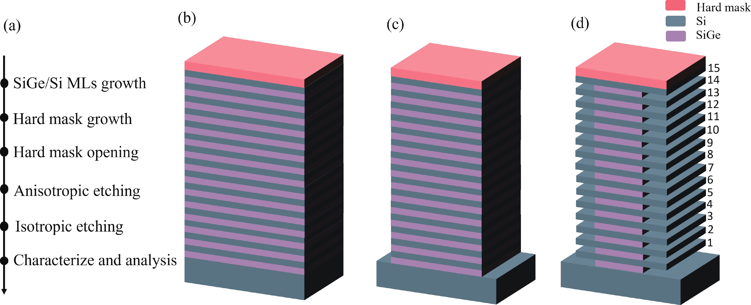
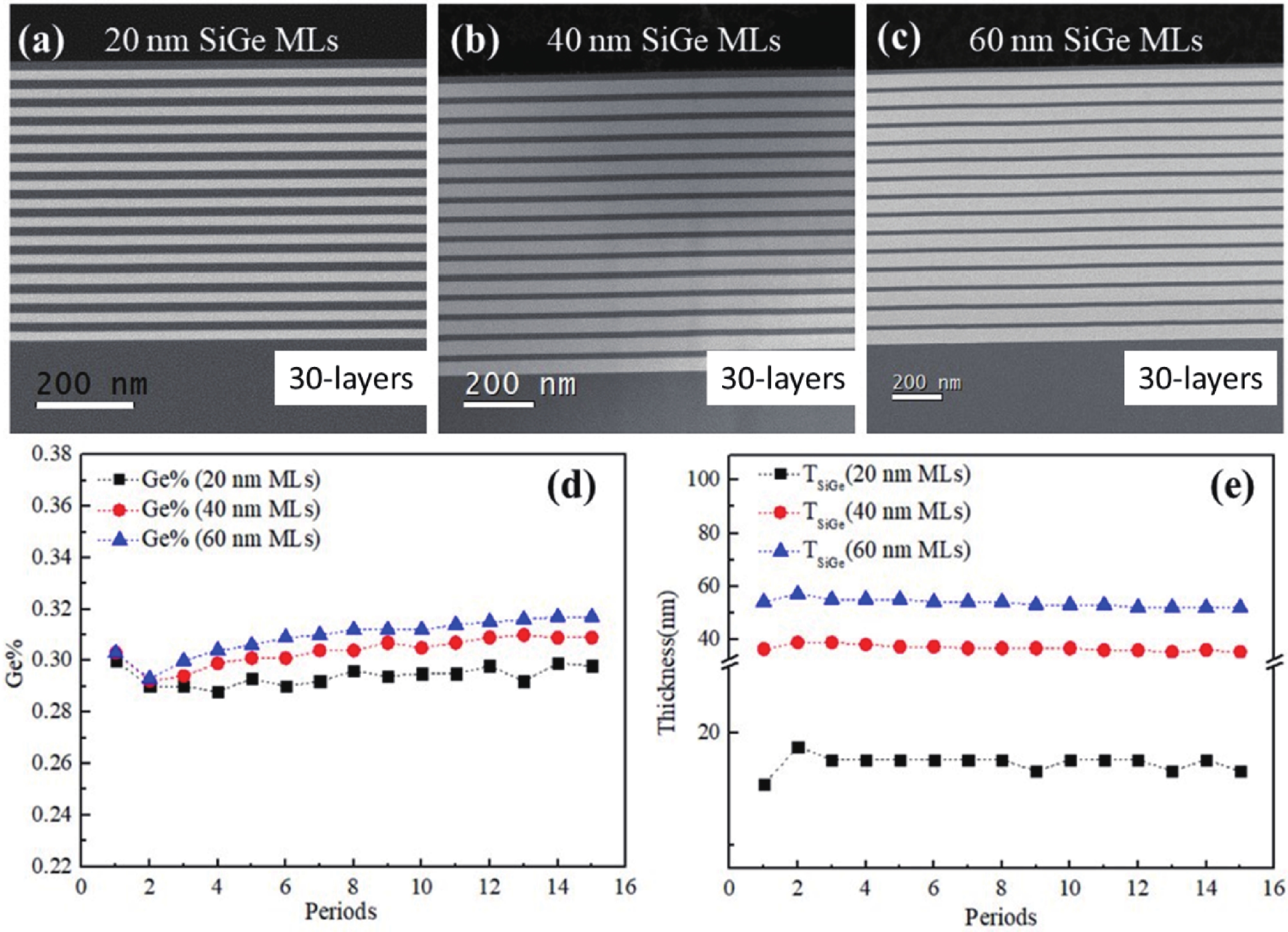
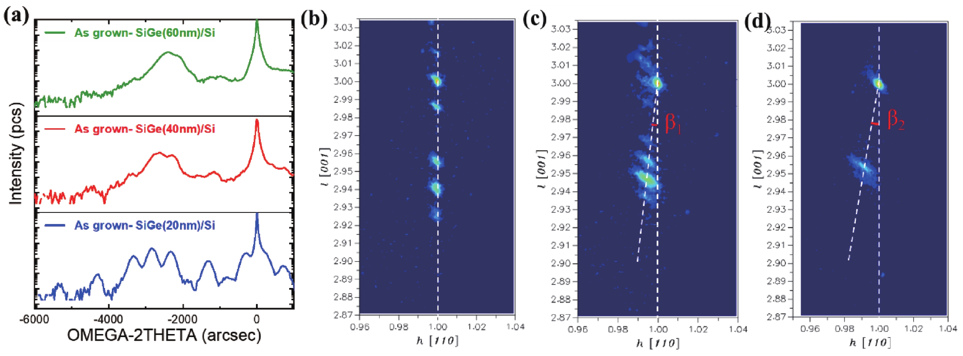
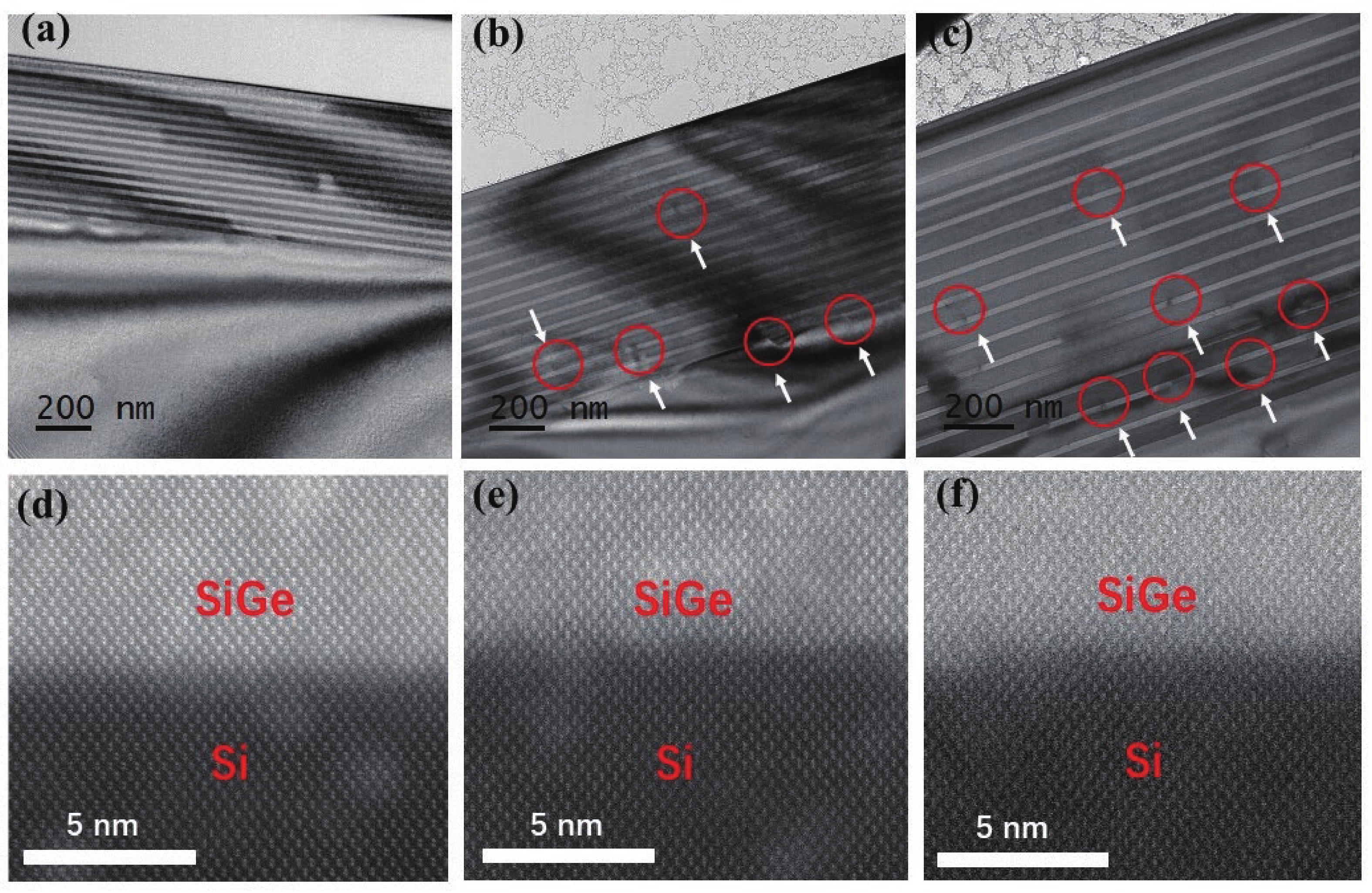
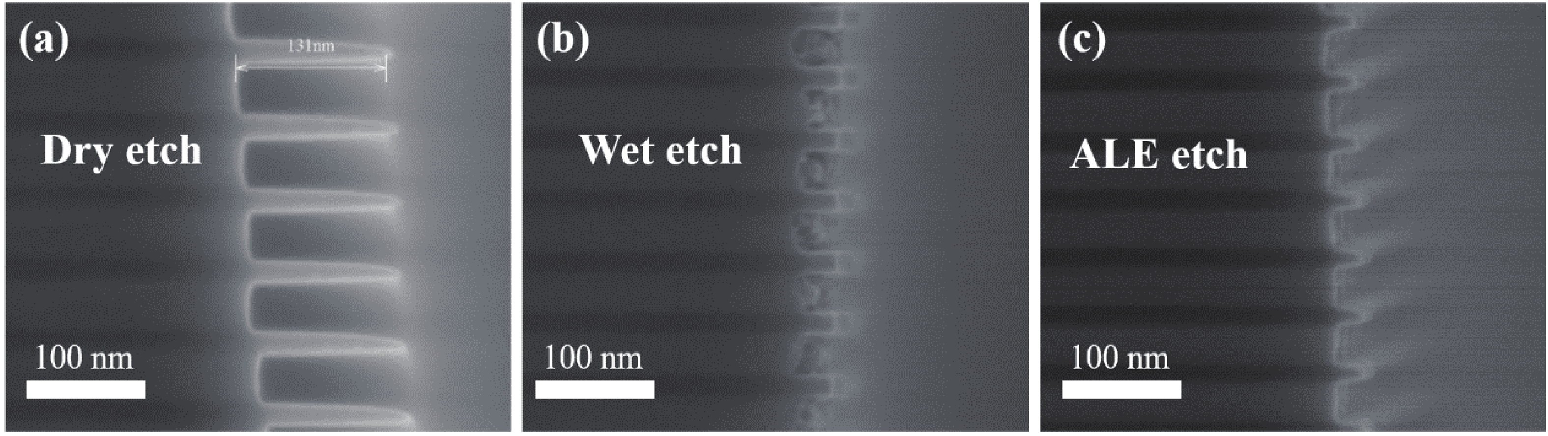
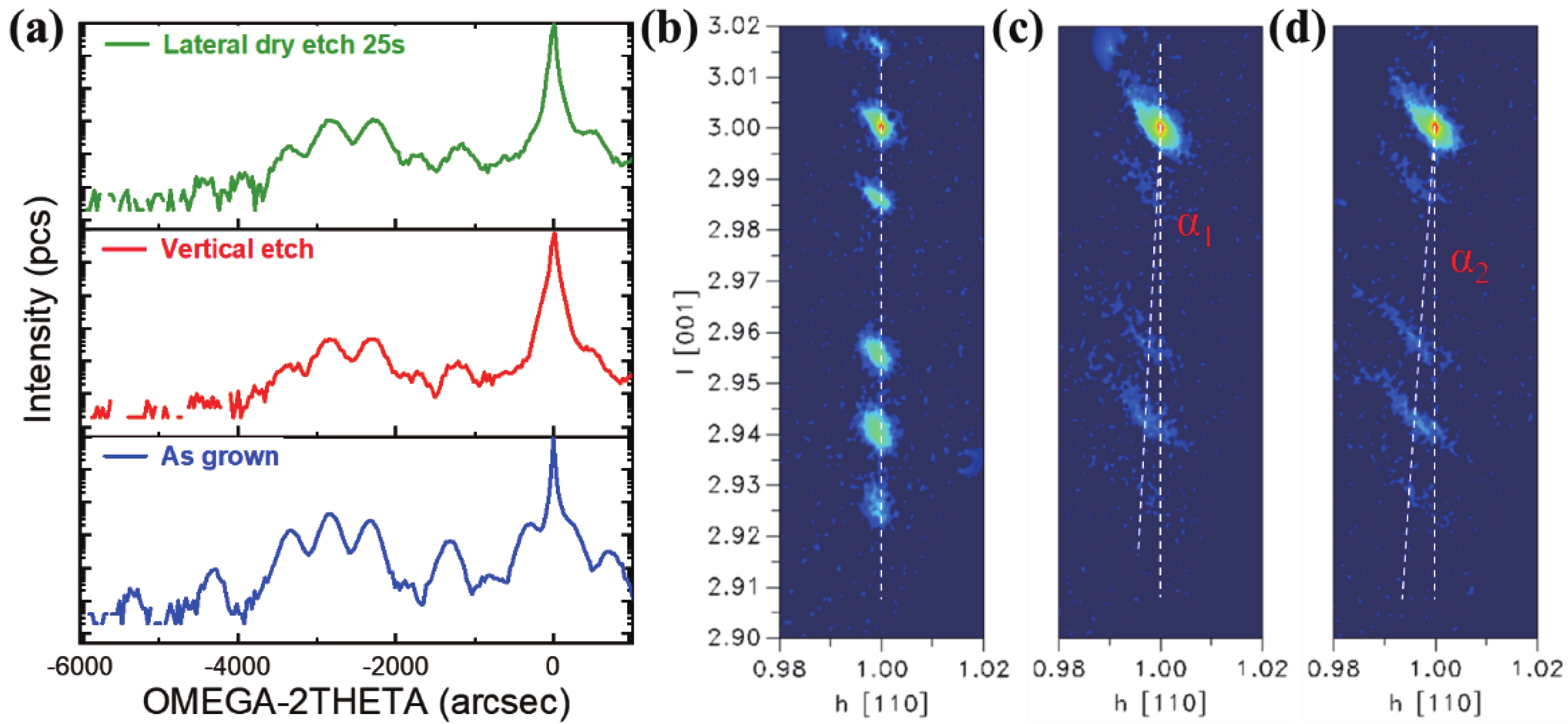
Table 1. Selective etches of SiGe to Si.
| Method | Solution | Advantages | Problem |
| Thermal etching | HCl[38−40] ClF3[41] |
High selectivity | React in chemical vapor deposition (CVD) tool The etching accuracy is limited Different etch rates for different crystal orientations |
| Dry etching | CF4/N2/O2[27] CF4/O2/He[20] NF3/O2/N2[42] |
Easy to use in large wafer size Isotropic Fast |
The etching accuracy is limited |
| Continuous wet etching | HF/HNO3/CH3COOH[25] HF/HNO3/CH3COOH/H2O[31] |
Excellent selectivity High etch rate Uniform etch rate in MLs etching |
Etch rate depends strongly on the Ge content Residues block the tunnel in MLs etching |
| HF/H2O2/CH3COOH[43−45] HF/H2O2/CH3COOH/H2O[46] |
High etch rate Nanoscale etching of SiGe to Si |
Not suitable for small size Long aging time |
|
| Wet ALE | H2O2/BOEs[47] HNO3/BOEs[48] |
Controllable etch rate Atomically smooth surfaces |
Long circle time Multistep processes Surface tension and capillary effect |
 DownLoad: CSV
| [1] |
Radamson H H, Zhu H L, Wu Z H, et al. State of the art and future perspectives in advanced CMOS technology. Nanomaterials (Basel), 2020, 10, 1555 doi: 10.3390/nano10081555
|
| [2] |
Radamson H H, Simeon E. CMOS past, present and future. Amsterdam: Elsevier, 2018, 105
|
| [3] |
Loubet N, Kal S, Alix C, et al. A novel dry selective etch of SiGe for the enablement of high performance logic stacked gate-all-around NanoSheet devices. 2019 IEEE International Electron Devices Meeting (IEDM), 2020, 11.4. 1 doi: 10.1109/IEDM19573.2019.8993615
|
| [4] |
Radamson H H, Zhang Y B, He X B, et al. The challenges of advanced CMOS process from 2D to 3D. Appl Sci, 2017, 7, 1047 doi: 10.3390/app7101047
|
| [5] |
Radamson H H, He X B, Zhang Q Z, et al. Miniaturization of cmos. Micromachines, 2019, 10, 293 doi: 10.3390/mi10050293
|
| [6] |
Radamson H H, Joelsson K B, Ni W X, et al. Characterization of highly boron-doped Si, Si1− xGe x and Ge layers by high-resolution transmission electron microscopy. J Cryst Growth, 1995, 157, 80 doi: 10.1016/0022-0248(95)00375-4
|
| [7] |
Wang G L, Luo J, Qin C L, et al. Integration of highly strained SiGe in source and drain with HK and MG for 22 nm bulk PMOS transistors. Nanoscale Res Lett, 2017, 12, 123 doi: 10.1186/s11671-017-1908-0
|
| [8] |
Singh N, Buddharaju K D, Manhas S K, et al. Si, SiGe nanowire devices by top–down technology and their applications. IEEE Trans Electron Devices, 2008, 55, 3107 doi: 10.1109/TED.2008.2005154
|
| [9] |
Barraud S, Previtali B, Lapras V, et al. Top-down fabrication and electrical characterization of Si and SiGe nanowires for advanced CMOS technologies. Semicond Sci Technol, 2019, 34, 074001 doi: 10.1088/1361-6641/ab1e5b
|
| [10] |
Radamson H H, Kolahdouz M. Selective epitaxy growth of Si1− xGe x layers for MOSFETs and FinFETs. J Mater Sci: Mater Electron, 2015, 26, 4584 doi: 10.1007/s10854-015-3123-z
|
| [11] |
Chu C L, Wu K, Luo G L, et al. Stacked Ge-nanosheet GAAFETs fabricated by Ge/Si multilayer epitaxy. IEEE Electron Device Lett, 2018, 39, 1133 doi: 10.1109/LED.2018.2850366
|
| [12] |
Veloso A, Paraschiv V, Vecchio E, et al. (invited) challenges on surface conditioning in 3D device architectures: Triple-gate FinFETs, gate-all-around lateral and vertical nanowire FETs. ECS Trans, 2017, 80, 3 doi: 10.1149/08002.0003ecst
|
| [13] |
Neisser M. International roadmap for devices and systems lithography roadmap. J Micro/nanopatterning Mater Metrol, 2021, 20, 44601 doi: 10.1117/1.JMM.20.4.044601
|
| [14] |
Ha D, Kim H S. Prospective innovation of DRAM, flash, and logic technologies for digital transformation (DX) era. 2022 IEEE Symposium on VLSI Technology and Circuits (VLSI Technology and Circuits), 2022, 417 doi: 10.1109/VLSITechnologyandCir46769.2022.9830465
|
| [15] |
Huang M, Si S F, He Z, et al. A 3D stackable 1T1C DRAM: Architecture, process integration and circuit simulation. 2023 IEEE International Memory Workshop (IMW), 2023, 1 doi: 10.1109/IMW56887.2023.10145931
|
| [16] |
Han J W, Park S H, Jeong M Y, et al. Ongoing evolution of DRAM scaling via third dimension-vertically stacked DRAM . 2023 IEEE Symposium on VLSI Technology and Circuits (VLSI Technology and Circuits), 2023, 1 doi: 10.23919/VLSITechnologyandCir57934.2023.10185290
|
| [17] |
Rachidi S, Campo A, Loup V, et al. Isotropic dry etching of Si selectively to Si0.7Ge0.3 for CMOS sub-10 nm applications. J Vac Sci Technol A Vac Surf Films, 2020, 38, 033002 doi: 10.1116/1.5143118
|
| [18] |
Huynh-Bao T, Sakhare S, Yakimets D, et al. A comprehensive benchmark and optimization of 5-nm lateral and vertical GAA 6T-SRAMs. IEEE Trans Electron Devices, 2016, 63, 643 doi: 10.1109/TED.2015.2504729
|
| [19] |
Liu Y C, Tu C T, Tsai C E, et al. First highly stacked Ge0.95Si0.05 nGAAFETs with record ION = 110 μA (4100 μA/μm) at VOV=VDS=0.5V and high Gm, max = 340 μS (13000 μS/μm) at VDS=0.5V by wet etching. 2021 Symposium on VLSI Technology, 2021, 1
|
| [20] |
Li J J, Wang W W, Li Y L, et al. Study of selective isotropic etching Si1− xGe x in process of nanowire transistors. J Mater Sci:Mater Electron, 2020, 31, 134 doi: 10.1007/s10854-019-02269-x
|
| [21] |
Lee S, Jeong J, Yoon J S, et al. Sensitivity of inner spacer thickness variations for sub-3-nm node silicon nanosheet field-effect transistors. Nanomaterials, 2022, 12, 3349 doi: 10.3390/nano12193349
|
| [22] |
Reboh S, Coquand R, Barraud S, et al. Strain, stress, and mechanical relaxation in fin-patterned Si/SiGe multilayers for sub-7 nm nanosheet gate-all-around device technology. Appl Phys Lett, 2018, 112, 051901 doi: 10.1063/1.5010997
|
| [23] |
Tuppen C G, Gibbings C J, Hockly M. Mismatch dislocation nucleation and propagation in Si/Si1− xGe x heterostructures. MRS Proc, 1988, 130, 185 doi: 10.1557/PROC-130-185
|
| [24] |
Barbisan L, Marzegalli A, Montalenti F. Atomic-scale insights on the formation of ordered arrays of edge dislocations in Ge/Si(001) films via molecular dynamics simulations. Sci Rep, 2022, 12, 3235 doi: 10.1038/s41598-022-07206-3
|
| [25] |
Orlowski M, Ndoye C, Liu T, et al. (invited) Si, SiGe, Ge, and III-V semiconductor nanomembranes and nanowires enabled by SiGe epitaxy. ECS Trans, 2010, 33, 777 doi: 10.1149/1.3487608
|
| [26] |
Borel S, Arvet C, Bilde J, et al. Isotropic etching of SiGe alloys with high selectivity to similar materials. Microelectron Eng, 2004, 73/74, 301 doi: 10.1016/S0167-9317(04)00115-7
|
| [27] |
Caubet V, Beylier C, Borel S, et al. Mechanisms of isotropic and selective etching between SiGe and Si. J Vac Sci Technol B Microelectron Nanometer Struct Process Meas Phenom, 2006, 24, 2748 doi: 10.1116/1.2393244
|
| [28] |
Zhao Y, Iwase T, Satake M, et al. Formation mechanism of rounded SiGe-etch front in isotropic SiGe plasma etching for gate-all-around FETs. IEEE J Electron Devices Soc, 2021, 9, 1112 doi: 10.1109/JEDS.2021.3130916
|
| [29] |
Chang W Y, Luo G L, Huang Y S, et al. SiGe and Si gate-all-around FET fabricated by selective etching the same epitaxial layers. 2022 6th IEEE Electron Devices Technology & Manufacturing Conference (EDTM), 2022, 21 doi: 10.1109/EDTM53872.2022.9797991
|
| [30] |
Wostyn K, Sebaai F, Rip J, et al. (invited) selective etch of Si and SiGe for gate all-around device architecture. ECS Trans, 2015, 69, 147 doi: 10.1149/06908.0147ecst
|
| [31] |
Choi Y, Jang H, Byun D S, et al. Selective chemical wet etching of Si1- xGe x versus Si in single-layer and multi-layer with HNO3/HF mixtures. Thin Solid Films, 2020, 709, 138230 doi: 10.1016/j.tsf.2020.138230
|
| [32] |
Kim S, Kim M, Ryu D, et al. Investigation of electrical characteristic behavior induced by channel-release process in stacked nanosheet gate-all-around MOSFETs. IEEE Trans Electron Devices, 2020, 67, 2648 doi: 10.1109/TED.2020.2989416
|
| [33] |
Zhuge J, Wang R S, Huang R, et al. Experimental investigation and design optimization guidelines of characteristic variability in silicon nanowire CMOS technology. 2009 IEEE International Electron Devices Meeting (IEDM), 2010, 1 doi: 10.1109/IEDM.2009.5424421
|
| [34] |
Sous S A, Hildmann B O, Kaysser W A. Characterization of dislocation densities in germanium and silicon single crystals by high resolution X-ray diffraction. Phys Stat Sol (a), 1997, 159, 343 doi: 10.1002/1521-396X(199702)159:2<343::AID-PSSA343>3.0.CO;2-#
|
| [35] |
Radamson H H, Moeen M, Abedin A, et al. Sensitivity of signal-to-noise ratio to the layer profile and crystal quality of SiGe/Si multilayers. ECS J Solid State Sci Technol, 2016, 5, P3196 doi: 10.1149/2.0261604jss
|
| [36] |
Hartmann J M, Papon A M, Barnes J P, et al. Growth kinetics of SiGe/Si superlattices on bulk and silicon-on-insulator substrates for multi-channel devices. J Cryst Growth, 2009, 311, 3152 doi: 10.1016/j.jcrysgro.2009.03.027
|
| [37] |
Radamson H H, Hållstedt J. Application of high-resolution X-ray diffraction for detecting defects in SiGe(C) materials. J Phys: Condens Matter, 2005, 17, S2315 doi: 10.1088/0953-8984/17/22/020
|
| [38] |
Destefanis V, Hartmann J M, Hopstaken M, et al. Low-thermal surface preparation, HCl etch and Si/SiGe selective epitaxy on (1 1 0) silicon surfaces. Semicond Sci Technol, 2008, 23, 105018 doi: 10.1088/0268-1242/23/10/105018
|
| [39] |
Loubet N, Kormann T, Chabanne G, et al. Selective etching of Si1− xGe x versus Si with gaseous HCl for the formation of advanced CMOS devices. Thin Solid Films, 2008, 517, 93 doi: 10.1016/j.tsf.2008.08.081
|
| [40] |
Mertens H, Ritzenthaler R, Hikavyy A, et al. Gate-all-around MOSFETs based on vertically stacked horizontal Si nanowires in a replacement metal gate process on bulk Si substrates. 2016 IEEE Symposium on VLSI Technology, 2016, 1 doi: 10.1109/VLSIT.2016.7573416
|
| [41] |
Tsai Y H, Wang M M. Fundamental study on the selective etching of SiGe and Si in ClF3 gas for nanosheet gate-all-around transistor manufacturing: A first principle study. J Vac Sci Technol B, 2022, 40, 013201 doi: 10.1116/6.0001455
|
| [42] |
Catano C, Joy N, Talone C, et al. Peculiarities of selective isotropic Si etch to SiGe for nanowire and GAA transistors. SPIE Advanced Lithography. Proc SPIE 10963, Advanced Etch Technology for Nanopatterning VIII, 2019, 1096, 72 doi: doi.org/10.1117/12.2514566
|
| [43] |
Cams T K, Tanner M O, Wang K L. Chemical etching of Si1– xGe x in HF : H2O2: CH3COOH. J Electrochem Soc, 1995, 142, 1260 doi: 10.1149/1.2044161
|
| [44] |
Holländer B, Buca D, Mantl S, et al. Wet chemical etching of Si, Si1– xGe x, and Ge in HF: H2O2: CH3COOH. J Electrochem Soc, 2010, 157, H643 doi: 10.1149/1.3382944
|
| [45] |
Pacco A, Tao Z, Rip J, et al. Scaled-down c-Si and c-SiGe wagon-wheels for the visualization of the anisotropy and selectivity of wet-chemical etchants. Nanoscale Res Lett, 2019, 14, 1 doi: 10.1186/s11671-018-2843-4
|
| [46] |
Baraissov Z, Pacco A, Koneti S, et al. Selective wet etching of silicon germanium in composite vertical nanowires. ACS Appl Mater Interfaces, 2019, 11, 36839 doi: 10.1021/acsami.9b11934
|
| [47] |
Yin X G, Zhu H L, Zhao L H, et al. Study of isotropic and Si-selective quasi atomic layer etching of Si1– xGe x. ECS J Solid State Sci Technol, 2020, 9, 034012 doi: 10.1149/2162-8777/ab80ae
|
| [48] |
Li Y Y, Zhu H L, Kong Z Z, et al. The effect of doping on the digital etching of silicon-selective silicon–germanium using nitric acids. Nanomaterials, 2021, 11, 1209 doi: 10.3390/nano11051209
|


Article views: 10862 Times PDF downloads: 1812 Times Cited by: 0 Times
Received: 07 July 2023 Revised: 05 August 2023 Online: Accepted Manuscript: 13 September 2023Uncorrected proof: 21 November 2023Published: 10 December 2023
| Citation: |
Zhenzhen Kong, Hongxiao Lin, Hailing Wang, Yanpeng Song, Junjie Li, Xiaomeng Liu, Anyan Du, Yuanhao Miao, Yiwen Zhang, Yuhui Ren, Chen Li, Jiahan Yu, Jinbiao Liu, Jingxiong Liu, Qinzhu Zhang, Jianfeng Gao, Huihui Li, Xiangsheng Wang, Junfeng Li, Henry H. Radamson, Chao Zhao, Tianchun Ye, Guilei Wang. Multiple SiGe/Si layers epitaxy and SiGe selective etching for vertically stacked DRAM[J]. Journal of Semiconductors, 2023, 44(12): 124101. doi: 10.1088/1674-4926/44/12/124101
****
Z Z Kong, H X Lin, H L Wang, Y P Song, J J Li, X M Liu, A Y Du, Y H Miao, Y W Zhang, Y H Ren, C Li, J H Yu, J B Liu, J X Liu, Q Z Zhang, J F Gao, H H Li, X S Wang, J F Li, H H Radamson, C Zhao, T C Ye, G L Wang. Multiple SiGe/Si layers epitaxy and SiGe selective etching for vertically stacked DRAM[J]. J. Semicond, 2023, 44(12): 124101. doi: 10.1088/1674-4926/44/12/124101

|
 Zhenzhen Kong received her BS in 2012. She is now a PhD student at University of Chinese Academy of Sciences under the supervision of Prof. Tianchun Ye, Prof. Henry H. Radamson and Prof. Guilei Wang. Her research focuses on growth of Group Ⅳ for high mobility ultra-thin body MOSFET and quantum computing devices
 Guilei Wang received his Bachelor's degree in 2005 and his PhD in 2016 from the University of Chinese Academy of Sciences. He has been worked as a professor at the Integrated Circuit Advanced Process Center at the Chinese Academy of Sciences until 2021. In October 2021, he joined the Beijing Superstring Academy of Memory Technology as a full professor. His research interests are focused on new materials, devices, and process integration for the IC industry
| [1] |
Radamson H H, Zhu H L, Wu Z H, et al. State of the art and future perspectives in advanced CMOS technology. Nanomaterials (Basel), 2020, 10, 1555 doi: 10.3390/nano10081555
|
| [2] |
Radamson H H, Simeon E. CMOS past, present and future. Amsterdam: Elsevier, 2018, 105
|
| [3] |
Loubet N, Kal S, Alix C, et al. A novel dry selective etch of SiGe for the enablement of high performance logic stacked gate-all-around NanoSheet devices. 2019 IEEE International Electron Devices Meeting (IEDM), 2020, 11.4. 1 doi: 10.1109/IEDM19573.2019.8993615
|
| [4] |
Radamson H H, Zhang Y B, He X B, et al. The challenges of advanced CMOS process from 2D to 3D. Appl Sci, 2017, 7, 1047 doi: 10.3390/app7101047
|
| [5] |
Radamson H H, He X B, Zhang Q Z, et al. Miniaturization of cmos. Micromachines, 2019, 10, 293 doi: 10.3390/mi10050293
|
| [6] |
Radamson H H, Joelsson K B, Ni W X, et al. Characterization of highly boron-doped Si, Si1− xGe x and Ge layers by high-resolution transmission electron microscopy. J Cryst Growth, 1995, 157, 80 doi: 10.1016/0022-0248(95)00375-4
|
| [7] |
Wang G L, Luo J, Qin C L, et al. Integration of highly strained SiGe in source and drain with HK and MG for 22 nm bulk PMOS transistors. Nanoscale Res Lett, 2017, 12, 123 doi: 10.1186/s11671-017-1908-0
|
| [8] |
Singh N, Buddharaju K D, Manhas S K, et al. Si, SiGe nanowire devices by top–down technology and their applications. IEEE Trans Electron Devices, 2008, 55, 3107 doi: 10.1109/TED.2008.2005154
|
| [9] |
Barraud S, Previtali B, Lapras V, et al. Top-down fabrication and electrical characterization of Si and SiGe nanowires for advanced CMOS technologies. Semicond Sci Technol, 2019, 34, 074001 doi: 10.1088/1361-6641/ab1e5b
|
| [10] |
Radamson H H, Kolahdouz M. Selective epitaxy growth of Si1− xGe x layers for MOSFETs and FinFETs. J Mater Sci: Mater Electron, 2015, 26, 4584 doi: 10.1007/s10854-015-3123-z
|
| [11] |
Chu C L, Wu K, Luo G L, et al. Stacked Ge-nanosheet GAAFETs fabricated by Ge/Si multilayer epitaxy. IEEE Electron Device Lett, 2018, 39, 1133 doi: 10.1109/LED.2018.2850366
|
| [12] |
Veloso A, Paraschiv V, Vecchio E, et al. (invited) challenges on surface conditioning in 3D device architectures: Triple-gate FinFETs, gate-all-around lateral and vertical nanowire FETs. ECS Trans, 2017, 80, 3 doi: 10.1149/08002.0003ecst
|
| [13] |
Neisser M. International roadmap for devices and systems lithography roadmap. J Micro/nanopatterning Mater Metrol, 2021, 20, 44601 doi: 10.1117/1.JMM.20.4.044601
|
| [14] |
Ha D, Kim H S. Prospective innovation of DRAM, flash, and logic technologies for digital transformation (DX) era. 2022 IEEE Symposium on VLSI Technology and Circuits (VLSI Technology and Circuits), 2022, 417 doi: 10.1109/VLSITechnologyandCir46769.2022.9830465
|
| [15] |
Huang M, Si S F, He Z, et al. A 3D stackable 1T1C DRAM: Architecture, process integration and circuit simulation. 2023 IEEE International Memory Workshop (IMW), 2023, 1 doi: 10.1109/IMW56887.2023.10145931
|
| [16] |
Han J W, Park S H, Jeong M Y, et al. Ongoing evolution of DRAM scaling via third dimension-vertically stacked DRAM . 2023 IEEE Symposium on VLSI Technology and Circuits (VLSI Technology and Circuits), 2023, 1 doi: 10.23919/VLSITechnologyandCir57934.2023.10185290
|
| [17] |
Rachidi S, Campo A, Loup V, et al. Isotropic dry etching of Si selectively to Si0.7Ge0.3 for CMOS sub-10 nm applications. J Vac Sci Technol A Vac Surf Films, 2020, 38, 033002 doi: 10.1116/1.5143118
|
| [18] |
Huynh-Bao T, Sakhare S, Yakimets D, et al. A comprehensive benchmark and optimization of 5-nm lateral and vertical GAA 6T-SRAMs. IEEE Trans Electron Devices, 2016, 63, 643 doi: 10.1109/TED.2015.2504729
|
| [19] |
Liu Y C, Tu C T, Tsai C E, et al. First highly stacked Ge0.95Si0.05 nGAAFETs with record ION = 110 μA (4100 μA/μm) at VOV=VDS=0.5V and high Gm, max = 340 μS (13000 μS/μm) at VDS=0.5V by wet etching. 2021 Symposium on VLSI Technology, 2021, 1
|
| [20] |
Li J J, Wang W W, Li Y L, et al. Study of selective isotropic etching Si1− xGe x in process of nanowire transistors. J Mater Sci:Mater Electron, 2020, 31, 134 doi: 10.1007/s10854-019-02269-x
|
| [21] |
Lee S, Jeong J, Yoon J S, et al. Sensitivity of inner spacer thickness variations for sub-3-nm node silicon nanosheet field-effect transistors. Nanomaterials, 2022, 12, 3349 doi: 10.3390/nano12193349
|
| [22] |
Reboh S, Coquand R, Barraud S, et al. Strain, stress, and mechanical relaxation in fin-patterned Si/SiGe multilayers for sub-7 nm nanosheet gate-all-around device technology. Appl Phys Lett, 2018, 112, 051901 doi: 10.1063/1.5010997
|
| [23] |
Tuppen C G, Gibbings C J, Hockly M. Mismatch dislocation nucleation and propagation in Si/Si1− xGe x heterostructures. MRS Proc, 1988, 130, 185 doi: 10.1557/PROC-130-185
|
| [24] |
Barbisan L, Marzegalli A, Montalenti F. Atomic-scale insights on the formation of ordered arrays of edge dislocations in Ge/Si(001) films via molecular dynamics simulations. Sci Rep, 2022, 12, 3235 doi: 10.1038/s41598-022-07206-3
|
| [25] |
Orlowski M, Ndoye C, Liu T, et al. (invited) Si, SiGe, Ge, and III-V semiconductor nanomembranes and nanowires enabled by SiGe epitaxy. ECS Trans, 2010, 33, 777 doi: 10.1149/1.3487608
|
| [26] |
Borel S, Arvet C, Bilde J, et al. Isotropic etching of SiGe alloys with high selectivity to similar materials. Microelectron Eng, 2004, 73/74, 301 doi: 10.1016/S0167-9317(04)00115-7
|
| [27] |
Caubet V, Beylier C, Borel S, et al. Mechanisms of isotropic and selective etching between SiGe and Si. J Vac Sci Technol B Microelectron Nanometer Struct Process Meas Phenom, 2006, 24, 2748 doi: 10.1116/1.2393244
|
| [28] |
Zhao Y, Iwase T, Satake M, et al. Formation mechanism of rounded SiGe-etch front in isotropic SiGe plasma etching for gate-all-around FETs. IEEE J Electron Devices Soc, 2021, 9, 1112 doi: 10.1109/JEDS.2021.3130916
|
| [29] |
Chang W Y, Luo G L, Huang Y S, et al. SiGe and Si gate-all-around FET fabricated by selective etching the same epitaxial layers. 2022 6th IEEE Electron Devices Technology & Manufacturing Conference (EDTM), 2022, 21 doi: 10.1109/EDTM53872.2022.9797991
|
| [30] |
Wostyn K, Sebaai F, Rip J, et al. (invited) selective etch of Si and SiGe for gate all-around device architecture. ECS Trans, 2015, 69, 147 doi: 10.1149/06908.0147ecst
|
| [31] |
Choi Y, Jang H, Byun D S, et al. Selective chemical wet etching of Si1- xGe x versus Si in single-layer and multi-layer with HNO3/HF mixtures. Thin Solid Films, 2020, 709, 138230 doi: 10.1016/j.tsf.2020.138230
|
| [32] |
Kim S, Kim M, Ryu D, et al. Investigation of electrical characteristic behavior induced by channel-release process in stacked nanosheet gate-all-around MOSFETs. IEEE Trans Electron Devices, 2020, 67, 2648 doi: 10.1109/TED.2020.2989416
|
| [33] |
Zhuge J, Wang R S, Huang R, et al. Experimental investigation and design optimization guidelines of characteristic variability in silicon nanowire CMOS technology. 2009 IEEE International Electron Devices Meeting (IEDM), 2010, 1 doi: 10.1109/IEDM.2009.5424421
|
| [34] |
Sous S A, Hildmann B O, Kaysser W A. Characterization of dislocation densities in germanium and silicon single crystals by high resolution X-ray diffraction. Phys Stat Sol (a), 1997, 159, 343 doi: 10.1002/1521-396X(199702)159:2<343::AID-PSSA343>3.0.CO;2-#
|
| [35] |
Radamson H H, Moeen M, Abedin A, et al. Sensitivity of signal-to-noise ratio to the layer profile and crystal quality of SiGe/Si multilayers. ECS J Solid State Sci Technol, 2016, 5, P3196 doi: 10.1149/2.0261604jss
|
| [36] |
Hartmann J M, Papon A M, Barnes J P, et al. Growth kinetics of SiGe/Si superlattices on bulk and silicon-on-insulator substrates for multi-channel devices. J Cryst Growth, 2009, 311, 3152 doi: 10.1016/j.jcrysgro.2009.03.027
|
| [37] |
Radamson H H, Hållstedt J. Application of high-resolution X-ray diffraction for detecting defects in SiGe(C) materials. J Phys: Condens Matter, 2005, 17, S2315 doi: 10.1088/0953-8984/17/22/020
|
| [38] |
Destefanis V, Hartmann J M, Hopstaken M, et al. Low-thermal surface preparation, HCl etch and Si/SiGe selective epitaxy on (1 1 0) silicon surfaces. Semicond Sci Technol, 2008, 23, 105018 doi: 10.1088/0268-1242/23/10/105018
|
| [39] |
Loubet N, Kormann T, Chabanne G, et al. Selective etching of Si1− xGe x versus Si with gaseous HCl for the formation of advanced CMOS devices. Thin Solid Films, 2008, 517, 93 doi: 10.1016/j.tsf.2008.08.081
|
| [40] |
Mertens H, Ritzenthaler R, Hikavyy A, et al. Gate-all-around MOSFETs based on vertically stacked horizontal Si nanowires in a replacement metal gate process on bulk Si substrates. 2016 IEEE Symposium on VLSI Technology, 2016, 1 doi: 10.1109/VLSIT.2016.7573416
|
| [41] |
Tsai Y H, Wang M M. Fundamental study on the selective etching of SiGe and Si in ClF3 gas for nanosheet gate-all-around transistor manufacturing: A first principle study. J Vac Sci Technol B, 2022, 40, 013201 doi: 10.1116/6.0001455
|
| [42] |
Catano C, Joy N, Talone C, et al. Peculiarities of selective isotropic Si etch to SiGe for nanowire and GAA transistors. SPIE Advanced Lithography. Proc SPIE 10963, Advanced Etch Technology for Nanopatterning VIII, 2019, 1096, 72 doi: doi.org/10.1117/12.2514566
|
| [43] |
Cams T K, Tanner M O, Wang K L. Chemical etching of Si1– xGe x in HF : H2O2: CH3COOH. J Electrochem Soc, 1995, 142, 1260 doi: 10.1149/1.2044161
|
| [44] |
Holländer B, Buca D, Mantl S, et al. Wet chemical etching of Si, Si1– xGe x, and Ge in HF: H2O2: CH3COOH. J Electrochem Soc, 2010, 157, H643 doi: 10.1149/1.3382944
|
| [45] |
Pacco A, Tao Z, Rip J, et al. Scaled-down c-Si and c-SiGe wagon-wheels for the visualization of the anisotropy and selectivity of wet-chemical etchants. Nanoscale Res Lett, 2019, 14, 1 doi: 10.1186/s11671-018-2843-4
|
| [46] |
Baraissov Z, Pacco A, Koneti S, et al. Selective wet etching of silicon germanium in composite vertical nanowires. ACS Appl Mater Interfaces, 2019, 11, 36839 doi: 10.1021/acsami.9b11934
|
| [47] |
Yin X G, Zhu H L, Zhao L H, et al. Study of isotropic and Si-selective quasi atomic layer etching of Si1– xGe x. ECS J Solid State Sci Technol, 2020, 9, 034012 doi: 10.1149/2162-8777/ab80ae
|
| [48] |
Li Y Y, Zhu H L, Kong Z Z, et al. The effect of doping on the digital etching of silicon-selective silicon–germanium using nitric acids. Nanomaterials, 2021, 11, 1209 doi: 10.3390/nano11051209
|
 23070008.pdf
|

|

 WeChat ID
Journal of Semiconductors © 2017 All Rights Reserved 京ICP备05085259号-2


