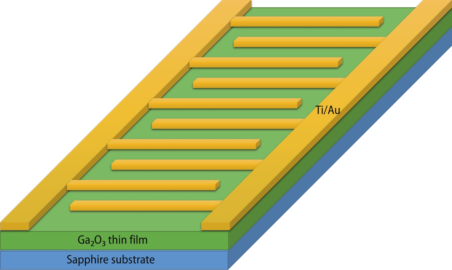
Fig. 1.
(Color online) Schematic diagram of solar-blind photodetector with MSM structure.
ARTICLES
Lijun Li, Chengkun Li, Shaoqing Wang, Qin Lu, Yifan Jia and Haifeng Chen
Corresponding author: Lijun Li, lilijun007@163.com
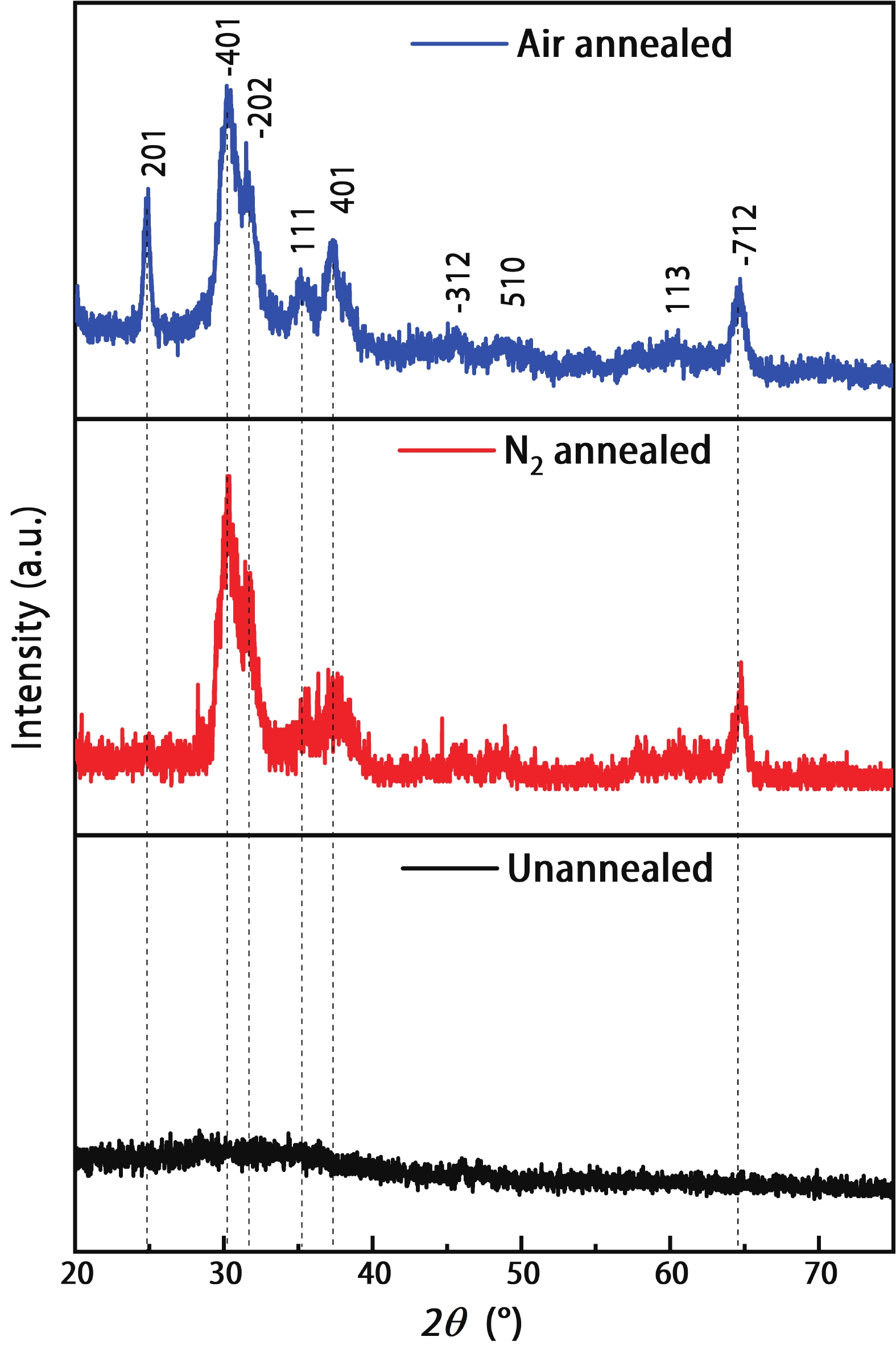
Abstract: Sn doping is an effective way to improve the response rate of Ga2O3 film based solar-blind detectors. In this paper, Sn-doped Ga2O3 films were prepared on a sapphire substrate by radio frequency magnetron sputtering. The films were characterized by X-ray diffraction, scanning electron microscopy, X-ray photoelectron spectroscopy and ultraviolet visible spectroscopy, and the effect of annealing atmosphere on the properties of films was studied. The Ga2O3 films changed from amorphous to β-Ga2O3 after annealing at 900 °C. The films were composed of micro crystalline particles with a diameter of about 5–20 nm. The β-Ga2O3 had high transmittance for wavelengths above 300 nm, and obvious absorption for solar-blind signals at 200–280 nm. The metal semiconductor metal type solar-blind detectors were prepared. The detector based on Sn-doped β-Ga2O3 thin film annealed in N2 has the best response performance to 254 nm light. The photo-current is 10 μA at 20 V, the dark-current is 5.76 pA, the photo dark current ratio is 1.7 × 10⁶, the response rate is 12.47 A/W, the external quantum efficiency is 6.09 × 10³%, the specific detection rate is 2.61 × 10¹² Jones, the response time and recovery time are 378 and 90 ms, respectively.
Keywords: Sn doped Ga2O3, RF magnetron sputtering, solar-blind photodetector
| [1] |
Xu J J, Zheng W, Huang F. Gallium oxide solar-blind ultraviolet photodetectors: A review. J Mater Chem C, 2019, 7, 8753 doi: 10.1039/C9TC02055A
|
| [2] |
Xie C, Lu X T, Tong X W, et al. Ultrawide-bandgap semiconductors: Recent progress in solar-blind deep-ultraviolet photodetectors based on inorganic ultrawide bandgap semiconductors. Adv Funct Mater, 2019, 29, 1970057 doi: 10.1002/adfm.201970057
|
| [3] |
Chen X H, Ren F F, Gu S L, et al. Review of gallium-oxide-based solar-blind ultraviolet photodetectors. Photon Res, 2019, 7, 381 doi: 10.1364/PRJ.7.000381
|
| [4] |
Wang J, Xiong Y Q, Ye L J, et al. Balanced performance for β-Ga2O3 solar blind photodetectors: The role of oxygen vacancies. Opt Mater, 2021, 112, 110808 doi: 10.1016/j.optmat.2021.110808
|
| [5] |
Oh Y Y, Ji J H, Kim S H, et al. Innovative Infrared-pulsed laser assisted RF sputtered β-Ga2O3 thin film at low temperature process. J Alloys Compd, 2021, 879, 160435 doi: 10.1016/j.jallcom.2021.160435
|
| [6] |
Guo D Y, Li P G, Chen Z W, et al. Ultra-wide bandgap semiconductor of β-Ga2O3 and its research progress of deep ultraviolet transparent electrode and solar-blind photodetector. Acta Phys Sin, 2019, 68, 078501 doi: 10.7498/aps.68.20181845
|
| [7] |
Xu R, Ma X C, Chen Y H, et al. Effect of oxygen vacancies in heteroepitaxial β-Ga2O3 thin film solar blind photodetectors. Mater Sci Semicond Process, 2022, 144, 106621 doi: 10.1016/j.mssp.2022.106621
|
| [8] |
Wu C, Wu F, Ma C, et al. A general strategy to ultrasensitive Ga2O3 based self-powered solar-blind photodetectors. Mater Today Phys, 2022, 23, 100643 doi: 10.1016/j.mtphys.2022.100643
|
| [9] |
Liu Z, Zhi Y S, Zhang S H, et al. Ultrahigh-performance planar β-Ga2O3 solar-blind Schottky photodiode detectors. Sci China Technol Sci, 2021, 64, 59 doi: 10.1007/s11431-020-1701-2
|
| [10] |
Zhang T, Li Y F, Cheng Q, et al. Influence of O2 pulse on the β-Ga2O3 films deposited by pulsed MOCVD. Ceram Int, 2022, 48, 8268 doi: 10.1016/j.ceramint.2021.12.031
|
| [11] |
Sasaki K, Higashiwaki M, Kuramata A, et al. MBE grown Ga2O3 and its power device applications. J Cryst Growth, 2013, 378, 591 doi: 10.1016/j.jcrysgro.2013.02.015
|
| [12] |
Liu W M, Zhu X D, He J B, et al. Atomic-layer-Ti-doped Ga2O3 thin films with tunable optical properties and wide ultraviolet optoelectronic responses. Phys Status Solidi RRL, 2021, 15, 2100411 doi: 10.1002/pssr.202100411
|
| [13] |
Gu L, Ma H P, Shen Y, et al. Temperature-dependent oxygen annealing effect on the properties of Ga2O3 thin film deposited by atomic layer deposition. J Alloys Compd, 2022, 925, 166727 doi: 10.1016/j.jallcom.2022.166727
|
| [14] |
Zhang X Y, Yang Y, Fan W H, et al. Growth and characterization of Si-doped Ga2O3 thin films by remote plasma atomic layer deposition: Toward UVC-LED application. Surf Coat Technol, 2022, 435, 128252 doi: 10.1016/j.surfcoat.2022.128252
|
| [15] |
Huang Y F, Deng G F, Saito K, et al. Current-controlled electroluminescence from light-emitting diodes based on Tm, Er, and Eu codoped Ga2O3 thin films. Appl Phys Express, 2022, 15, 081005 doi: 10.35848/1882-0786/ac851d
|
| [16] |
Zhang J Y, Willis J, Yang Z N, et al. Deep UV transparent conductive oxide thin films realized through degenerately doped wide-bandgap gallium oxide. Cell Rep Phys Sci, 2022, 3, 100801 doi: 10.1016/j.xcrp.2022.100801
|
| [17] |
Wu C, Guo D Y, Zhang L Y, et al. Systematic investigation of the growth kinetics of β-Ga2O3 epilayer by plasma enhanced chemical vapor deposition. Appl Phys Lett, 2020, 116, 072102 doi: 10.1063/1.5142196
|
| [18] |
Hou X H, Zhao X L, Zhang Y, et al. High-performance harsh-environment-resistant GaOx solar-blind photodetectors via defect and doping engineering. Adv Mater, 2022, 34, 2270009 doi: 10.1002/adma.202270009
|
| [19] |
Gu K Y, Zhang Z L, Tang K, et al. Effect of a seed layer on microstructure and electrical properties of Ga2O3 films on variously oriented Si substrates. Vacuum, 2022, 195, 110671 doi: 10.1016/j.vacuum.2021.110671
|
| [20] |
Li S F, Jiao S J, Wang D B, et al. The influence of sputtering power on the structural, morphological and optical properties of β-Ga2O3 thin films. J Alloys Compd, 2018, 753, 186 doi: 10.1016/j.jallcom.2018.04.196
|
| [21] |
Singh A K, Yadav S, Kulriya P K, et al. Sapphire substrate induced effects on β-Ga2O3 thin films. J Mater Sci:Mater Electron, 2022, 33, 12629 doi: 10.1007/s10854-022-08212-x
|
| [22] |
Zhang T, Guan D G, Liu N T, et al. Room temperature fabrication and post-annealing treatment of amorphous Ga2O3 photodetectors for deep-ultraviolet light detection. Appl Phys Express, 2022, 15, 022007 doi: 10.35848/1882-0786/ac48d9
|
| [23] |
Li S F. Study on GaO thin films prepared by magnetron sputtering and their photoelectric properties. M. S. Dissertation, Harbin Institute of Technology, 2018 (in Chinese)
|
| [24] |
Mi W, Li Z, Luan C N, et al. Transparent conducting tin-doped Ga2O3 films deposited on MgAl2O4 (100) substrates by MOCVD. Ceram Int, 2015, 41, 2572 doi: 10.1016/j.ceramint.2014.11.004
|
| [25] |
Feng Q J, Dong Z J, Liu W, et al. High responsivity solar-blind UV photodetector based on single centimeter-sized Sn-doped β-Ga2O3 microwire. Micro Nanostructures, 2022, 167, 207255 doi: 10.1016/j.micrna.2022.207255
|
| [26] |
Zhao X L, Cui W, Wu Z P, et al. Growth and characterization of Sn doped β-Ga2O3 thin films and enhanced performance in a solar-blind photodetector. J Electron Mater, 2017, 46, 2366 doi: 10.1007/s11664-017-5291-5
|
| [27] |
Hou S, Liu Q, Xing Z Y, et al. Effect of Sn doping on the performance of Ga2O3 based solar blind UV detector. Opto-Electr Engineering, 2019, 46, 190011 doi: 10.12086/oee.2019.190011
|
| [28] |
Fan M M, Lu Y J, Xu K L, et al. Growth and characterization of Sn-doped β-Ga2O3 thin films by chemical vapor deposition using solid powder precursors toward solar-blind ultraviolet photodetection. Appl Surf Sci, 2020, 509, 144867 doi: 10.1016/j.apsusc.2019.144867
|
| [29] |
Shen Y, Ma H P, Gu L, et al. Atomic-level Sn doping effect in Ga2O3 films using plasma-enhanced atomic layer deposition. Nanomaterials, 2022, 12, 4256 doi: 10.3390/nano12234256
|
| [30] |
Du X J, Li Z, Luan C N, et al. Preparation and characterization of Sn-doped β-Ga2O3 homoepitaxial films by MOCVD. J Mater Sci, 2015, 50, 3252 doi: 10.1007/s10853-015-8893-4
|
| [31] |
Yang Y, Liu W M, Huang T T, et al. Low deposition temperature amorphous ALD-Ga2O3 thin films and decoration with MoS2 multilayers toward flexible solar-blind photodetectors. ACS Appl Mater Interfaces, 2021, 13, 41802 doi: 10.1021/acsami.1c11692
|
| [32] |
Tao J J, Lu H L, Gu Y, et al. Investigation of growth characteristics, compositions, and properties of atomic layer deposited amorphous Zn-doped Ga2O3 films. Appl Surf Sci, 2019, 476, 733 doi: 10.1016/j.apsusc.2019.01.177
|
| [33] |
Ma H L, Su Q. Effect of oxygen pressure on structure and optical band gap of gallium oxide thin films prepared by sputtering. Acta Phys Sin, 2014, 63, 116701 doi: 10.7498/aps.63.116701
|
| [34] |
Li Z M, Jiao T, Li W C, et al. Solar-blind ultraviolet photodetectors based on homoepitaxial β-Ga2O3 films. Opt Mater, 2021, 122, 111665 doi: 10.1016/j.optmat.2021.111665
|
| [35] |
Liu Z, Zhang M L, Yang L L, et al. Enhancement-mode normally-off β-Ga2O3: Si metal-semiconductor field-effect deep-ultraviolet phototransistor. Semicond Sci Technol, 2022, 37, 015001 doi: 10.1088/1361-6641/ac38bd
|
| [36] |
Pratiyush A S, Krishnamoorthy S, Kumar S, et al. Demonstration of zero bias responsivity in MBE grown β-Ga2O3 lateral deep-UV photodetector. Jpn J Appl Phys, 2018, 57, 060313 doi: 10.7567/JJAP.57.060313
|
| [37] |
Arora K, Goel N, Kumar M, et al. Ultrahigh performance of self-powered β-Ga2O3 thin film solar-blind photodetector grown on cost-effective Si substrate using high-temperature seed layer. ACS Photonics, 2018, 5, 2391 doi: 10.1021/acsphotonics.8b00174
|
| [38] |
Xu Y, Chen X H, Zhang Y F, et al. Fast speed Ga2O3 solar-blind Schottky photodiodes with large sensitive area. IEEE Electron Device Lett, 2020, 41, 997 doi: 10.1109/LED.2020.2998804
|
| [39] |
Kalita G, Mahyavanshi R D, Desai P, et al. Photovoltaic action in graphene –Ga 2O3 heterojunction with deep-ultraviolet irradiation. Phys Status Solidi R, 2018, 12, 1800198 doi: 10.1002/pssr.201800198
|
| [40] |
Chen M Z, Ma J G, Li P, et al. Zero-biased deep ultraviolet photodetectors based on graphene/cleaved (100) Ga2O3 heterojunction. Opt Express, 2019, 27, 8717 doi: 10.1364/OE.27.008717
|
| [41] |
Wu C, He C, Guo D, et al. Vertical α/β-Ga2O3 phase junction nanorods array with graphene-silver nanowire hybrid conductive electrode for high-performance self-powered solar-blind photodetectors. Mater Today Phys, 2020, 12, 100193 doi: 10.1016/j.mtphys.2020.100193
|
| [42] |
Chen K, Wang S L, He C R, et al. Photoelectrochemical self-powered solar-blind photodetectors based on Ga2O3 nanorod array/electrolyte solid/liquid heterojunctions with a large separation interface of photogenerated carriers. ACS Appl Nano Mater, 2019, 2, 6169 doi: 10.1021/acsanm.9b00992
|
| [43] |
Wu C, Wu F M, Hu H Z, et al. Work function tunable laser induced graphene electrodes for Schottky type solar-blind photodetectors. Appl Phys Lett, 2022, 120, 101102 doi: 10.1063/5.0080855
|
| [44] |
Huang L, Feng Q, Han G Q, et al. Comparison study of β-Ga2O3 photodetectors grown on sapphire at different oxygen pressures. IEEE Photonics J, 2017, 9, 1 doi: 10.1109/JPHOT.2017.2731625
|
| [45] |
Liu X Z, Liu Q, Zhao B W, et al. Comparison of β-Ga2O3 thin films grown on r-plane and c-plane sapphire substrates. Vacuum, 2020, 178, 109435 doi: 10.1016/j.vacuum.2020.109435
|
| [46] |
Wang Q L, Chen J, Huang P, et al. Influence of growth temperature on the characteristics of β-Ga2O3 epitaxial films and related solar-blind photodetectors. Appl Surf Sci, 2019, 489, 101 doi: 10.1016/j.apsusc.2019.05.328
|
| [47] |
He C R, Guo D Y, Chen K, et al. α-Ga2O3 nanorod array–Cu2O microsphere p–n junctions for self-powered spectrum-distinguishable photodetectors. ACS Appl Nano Mater, 2019, 2, 4095 doi: 10.1021/acsanm.9b00527
|
| [48] |
Guo D, Chen K, Wang S, et al. Self-powered solar-blind photodetectors based on α/β phase junction of Ga2O3. Phys Rev Appl, 2020, 13, 024051 doi: 10.1103/PhysRevApplied.13.024051
|
| [49] |
Wu C, Wu F M, Hu H Z, et al. Review of self-powered solar-blind photodetectors based on Ga2O3. Mater Today Phys, 2022, 28, 100883 doi: 10.1016/j.mtphys.2022.100883
|
| [50] |
Kaur D, Kumar M. A strategic review on gallium oxide based deep-ultraviolet photodetectors: Recent progress and future prospects. Adv Optical Mater, 2021, 9, 2002160 doi: 10.1002/adom.202002160
|
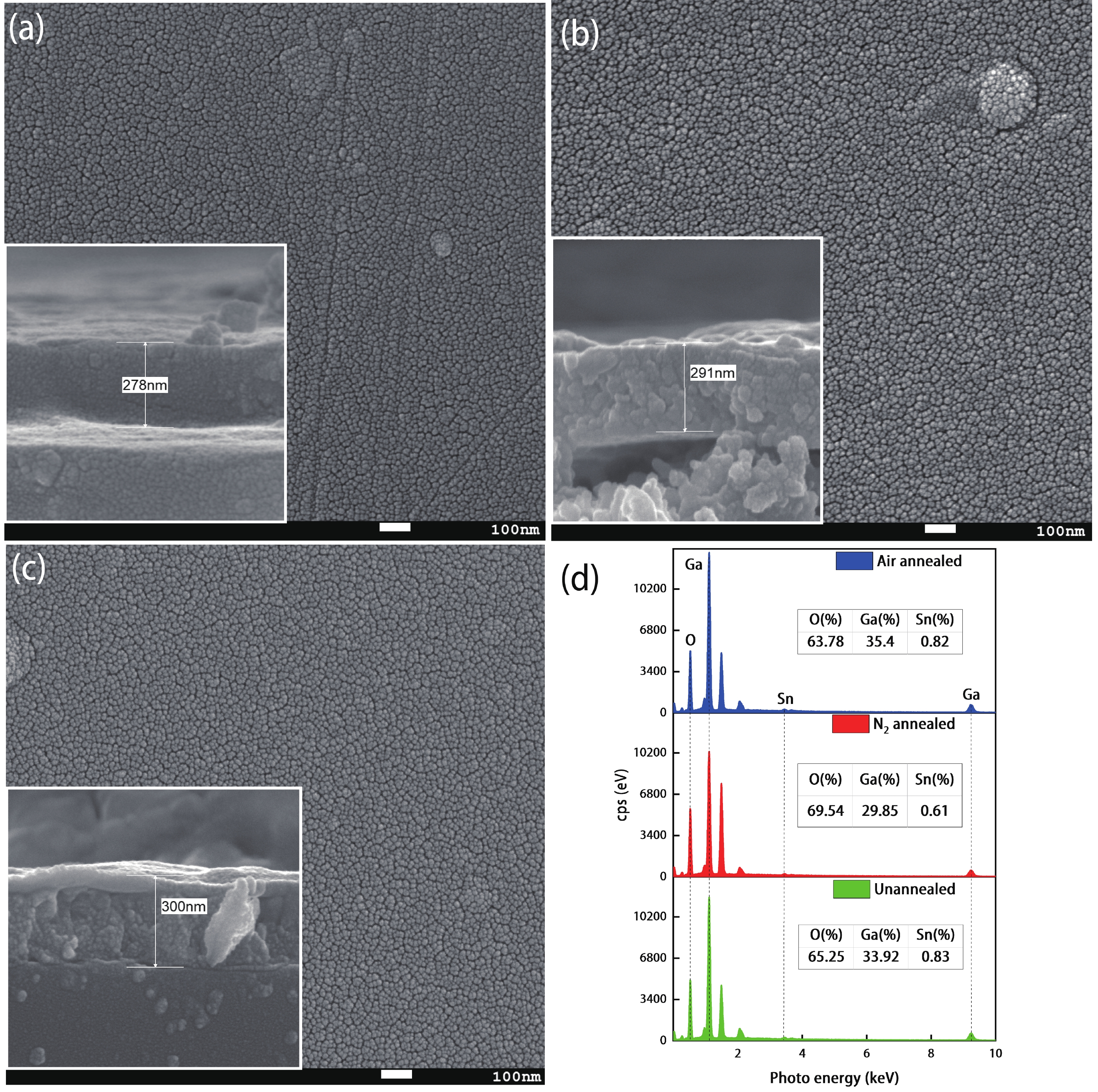
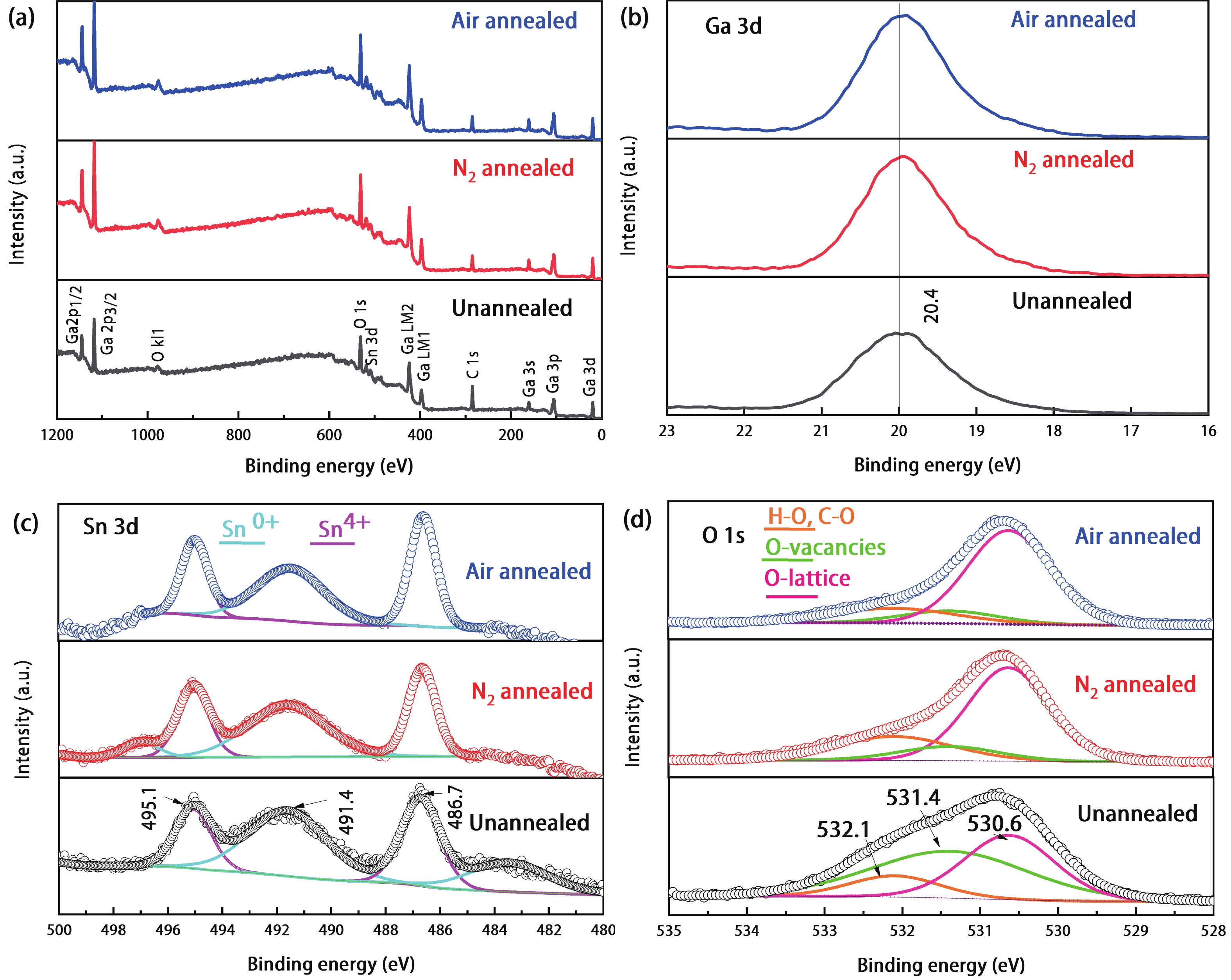
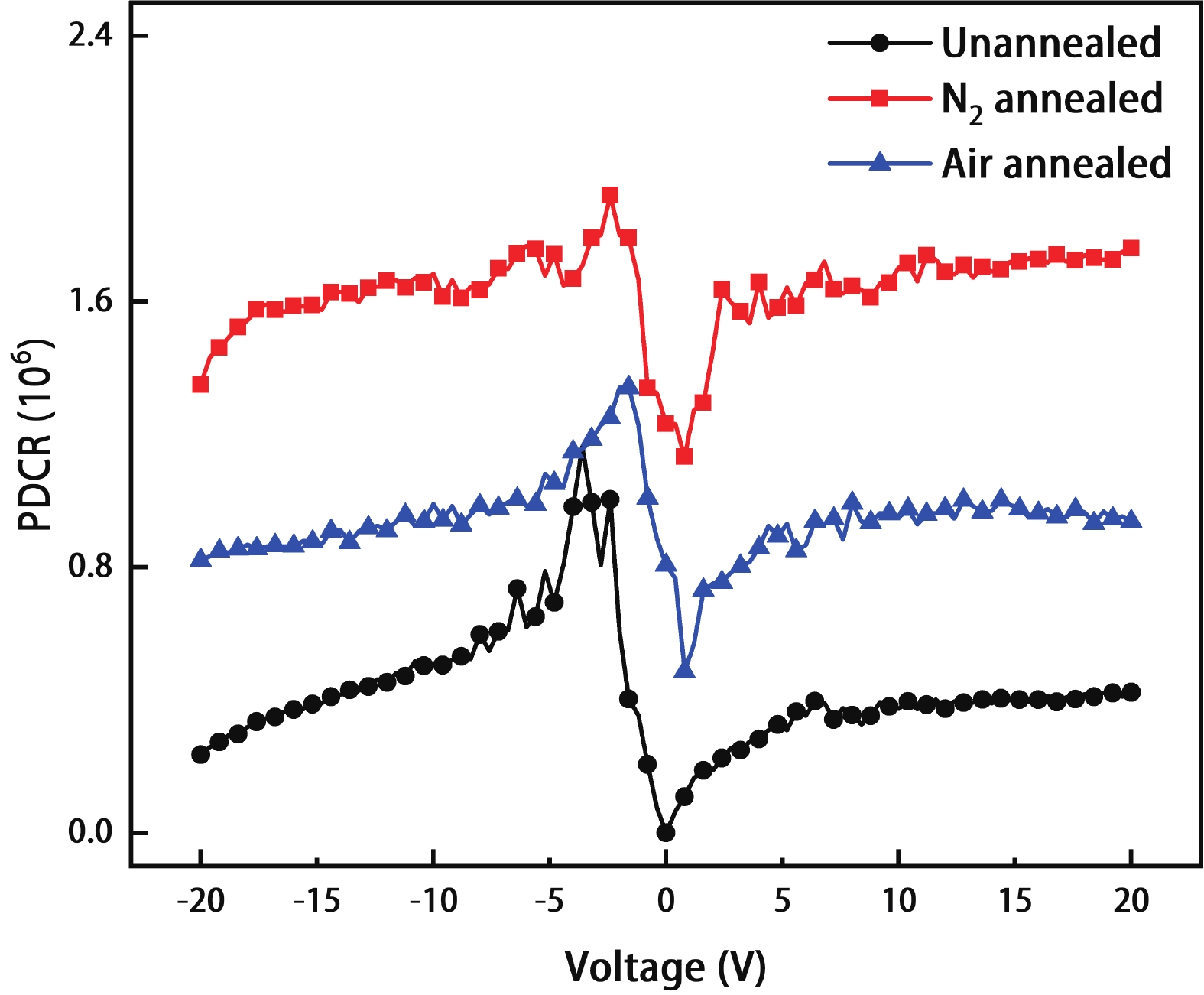
Table 1. Key parameters of Ga2O3 thin film photoelectric detector.
| Material | Structure | PDCR | R (A/W) | EQE (%) | D* (Jones) | τr/τd | Ref. |
| Ni/Au/β-Ga2O3 | MSM | 103 | 1.4 × 10⁻³ | 0.5 | 2.0 × 10¹² | 1.1 s/0.3 s | [36] |
| Au/β-Ga2O3/Si | MSM | 6.13 | 96.13 | 4.77 × 10⁴ | – | 32 ms/78 ms | [37] |
| Ni/Au/β-Ga2O3/Ti/Au | MSM | 104 | 9.78 | 4.25 × 10³ | 3.92 × 10¹⁴ | 5.19 μs | [38] |
| Au/Graphene/β-Ga2O3/In | MSM | – | 6.1 | 2.98 × 10³ | – | 0.62 s/0.67 s | [39] |
| Graphene/β-Ga2O3 wafer | MSM | 2.28 × 10² | 0.01 | 5 | – | 30 ns/2.24 μs | [40] |
| α/β-Ga2O3 NRAS | PEC | 2.0 × 10³ | 2.6 × 10⁻⁴ | – | 2.8 × 10⁹ | 0.54 s/1.63 s | [41] |
| β-Ga2O3 NRAS | PEC | 28.97 | 3.8 × 10⁻³ | 1.86 | 0.29 s/0.16 s | [42] | |
| LIG(Graphene)/Ga2O3 | – | 3.72 × 10³ | 0.043 | – | 6.73 × 10¹² | 0.4 s/0.06 s | [43] |
| Ti/Au/β-Ga2O3 | MSM | 510 | 0.06 | 28.3 | – | 2.92 s/2.97 s | [44] |
| Ti/Au/β-Ga2O3 | MSM | 773 | 91.9 | – | 7.2 × 10¹³ | 5.4 s/2.1 s | [45] |
| Au/β-Ga2O3/Au | MSM | 1.6 × 10³ | 18.23 | – | – | 0.44 s/0.72 s | [46] |
| α-Ga2O3/Cu2O | PEC | – | 4.2 × 10⁻⁴ | – | – | 10.3 s/10.1 s | [47] |
| MSM@Unannealed | 4.21 × 10⁵ | 1.86 | 9.08 × 10² | 4.94 × 10¹¹ | 0.54 s/0.6 s | ||
| β-Ga2O3 thin films | MSM@N2 annealed | 1.75 × 10⁶ | 12.47 | 6.09 × 10³ | 2.61 × 10¹² | 0.37 s/0.09 s | This work |
| MSM@Air annealed | 9.44 × 10⁵ | 8.56 | 4.18 × 10³ | 1.59 × 10¹² | 0.39 s/0.12 s |
 DownLoad: CSV
| [1] |
Xu J J, Zheng W, Huang F. Gallium oxide solar-blind ultraviolet photodetectors: A review. J Mater Chem C, 2019, 7, 8753 doi: 10.1039/C9TC02055A
|
| [2] |
Xie C, Lu X T, Tong X W, et al. Ultrawide-bandgap semiconductors: Recent progress in solar-blind deep-ultraviolet photodetectors based on inorganic ultrawide bandgap semiconductors. Adv Funct Mater, 2019, 29, 1970057 doi: 10.1002/adfm.201970057
|
| [3] |
Chen X H, Ren F F, Gu S L, et al. Review of gallium-oxide-based solar-blind ultraviolet photodetectors. Photon Res, 2019, 7, 381 doi: 10.1364/PRJ.7.000381
|
| [4] |
Wang J, Xiong Y Q, Ye L J, et al. Balanced performance for β-Ga2O3 solar blind photodetectors: The role of oxygen vacancies. Opt Mater, 2021, 112, 110808 doi: 10.1016/j.optmat.2021.110808
|
| [5] |
Oh Y Y, Ji J H, Kim S H, et al. Innovative Infrared-pulsed laser assisted RF sputtered β-Ga2O3 thin film at low temperature process. J Alloys Compd, 2021, 879, 160435 doi: 10.1016/j.jallcom.2021.160435
|
| [6] |
Guo D Y, Li P G, Chen Z W, et al. Ultra-wide bandgap semiconductor of β-Ga2O3 and its research progress of deep ultraviolet transparent electrode and solar-blind photodetector. Acta Phys Sin, 2019, 68, 078501 doi: 10.7498/aps.68.20181845
|
| [7] |
Xu R, Ma X C, Chen Y H, et al. Effect of oxygen vacancies in heteroepitaxial β-Ga2O3 thin film solar blind photodetectors. Mater Sci Semicond Process, 2022, 144, 106621 doi: 10.1016/j.mssp.2022.106621
|
| [8] |
Wu C, Wu F, Ma C, et al. A general strategy to ultrasensitive Ga2O3 based self-powered solar-blind photodetectors. Mater Today Phys, 2022, 23, 100643 doi: 10.1016/j.mtphys.2022.100643
|
| [9] |
Liu Z, Zhi Y S, Zhang S H, et al. Ultrahigh-performance planar β-Ga2O3 solar-blind Schottky photodiode detectors. Sci China Technol Sci, 2021, 64, 59 doi: 10.1007/s11431-020-1701-2
|
| [10] |
Zhang T, Li Y F, Cheng Q, et al. Influence of O2 pulse on the β-Ga2O3 films deposited by pulsed MOCVD. Ceram Int, 2022, 48, 8268 doi: 10.1016/j.ceramint.2021.12.031
|
| [11] |
Sasaki K, Higashiwaki M, Kuramata A, et al. MBE grown Ga2O3 and its power device applications. J Cryst Growth, 2013, 378, 591 doi: 10.1016/j.jcrysgro.2013.02.015
|
| [12] |
Liu W M, Zhu X D, He J B, et al. Atomic-layer-Ti-doped Ga2O3 thin films with tunable optical properties and wide ultraviolet optoelectronic responses. Phys Status Solidi RRL, 2021, 15, 2100411 doi: 10.1002/pssr.202100411
|
| [13] |
Gu L, Ma H P, Shen Y, et al. Temperature-dependent oxygen annealing effect on the properties of Ga2O3 thin film deposited by atomic layer deposition. J Alloys Compd, 2022, 925, 166727 doi: 10.1016/j.jallcom.2022.166727
|
| [14] |
Zhang X Y, Yang Y, Fan W H, et al. Growth and characterization of Si-doped Ga2O3 thin films by remote plasma atomic layer deposition: Toward UVC-LED application. Surf Coat Technol, 2022, 435, 128252 doi: 10.1016/j.surfcoat.2022.128252
|
| [15] |
Huang Y F, Deng G F, Saito K, et al. Current-controlled electroluminescence from light-emitting diodes based on Tm, Er, and Eu codoped Ga2O3 thin films. Appl Phys Express, 2022, 15, 081005 doi: 10.35848/1882-0786/ac851d
|
| [16] |
Zhang J Y, Willis J, Yang Z N, et al. Deep UV transparent conductive oxide thin films realized through degenerately doped wide-bandgap gallium oxide. Cell Rep Phys Sci, 2022, 3, 100801 doi: 10.1016/j.xcrp.2022.100801
|
| [17] |
Wu C, Guo D Y, Zhang L Y, et al. Systematic investigation of the growth kinetics of β-Ga2O3 epilayer by plasma enhanced chemical vapor deposition. Appl Phys Lett, 2020, 116, 072102 doi: 10.1063/1.5142196
|
| [18] |
Hou X H, Zhao X L, Zhang Y, et al. High-performance harsh-environment-resistant GaOx solar-blind photodetectors via defect and doping engineering. Adv Mater, 2022, 34, 2270009 doi: 10.1002/adma.202270009
|
| [19] |
Gu K Y, Zhang Z L, Tang K, et al. Effect of a seed layer on microstructure and electrical properties of Ga2O3 films on variously oriented Si substrates. Vacuum, 2022, 195, 110671 doi: 10.1016/j.vacuum.2021.110671
|
| [20] |
Li S F, Jiao S J, Wang D B, et al. The influence of sputtering power on the structural, morphological and optical properties of β-Ga2O3 thin films. J Alloys Compd, 2018, 753, 186 doi: 10.1016/j.jallcom.2018.04.196
|
| [21] |
Singh A K, Yadav S, Kulriya P K, et al. Sapphire substrate induced effects on β-Ga2O3 thin films. J Mater Sci:Mater Electron, 2022, 33, 12629 doi: 10.1007/s10854-022-08212-x
|
| [22] |
Zhang T, Guan D G, Liu N T, et al. Room temperature fabrication and post-annealing treatment of amorphous Ga2O3 photodetectors for deep-ultraviolet light detection. Appl Phys Express, 2022, 15, 022007 doi: 10.35848/1882-0786/ac48d9
|
| [23] |
Li S F. Study on GaO thin films prepared by magnetron sputtering and their photoelectric properties. M. S. Dissertation, Harbin Institute of Technology, 2018 (in Chinese)
|
| [24] |
Mi W, Li Z, Luan C N, et al. Transparent conducting tin-doped Ga2O3 films deposited on MgAl2O4 (100) substrates by MOCVD. Ceram Int, 2015, 41, 2572 doi: 10.1016/j.ceramint.2014.11.004
|
| [25] |
Feng Q J, Dong Z J, Liu W, et al. High responsivity solar-blind UV photodetector based on single centimeter-sized Sn-doped β-Ga2O3 microwire. Micro Nanostructures, 2022, 167, 207255 doi: 10.1016/j.micrna.2022.207255
|
| [26] |
Zhao X L, Cui W, Wu Z P, et al. Growth and characterization of Sn doped β-Ga2O3 thin films and enhanced performance in a solar-blind photodetector. J Electron Mater, 2017, 46, 2366 doi: 10.1007/s11664-017-5291-5
|
| [27] |
Hou S, Liu Q, Xing Z Y, et al. Effect of Sn doping on the performance of Ga2O3 based solar blind UV detector. Opto-Electr Engineering, 2019, 46, 190011 doi: 10.12086/oee.2019.190011
|
| [28] |
Fan M M, Lu Y J, Xu K L, et al. Growth and characterization of Sn-doped β-Ga2O3 thin films by chemical vapor deposition using solid powder precursors toward solar-blind ultraviolet photodetection. Appl Surf Sci, 2020, 509, 144867 doi: 10.1016/j.apsusc.2019.144867
|
| [29] |
Shen Y, Ma H P, Gu L, et al. Atomic-level Sn doping effect in Ga2O3 films using plasma-enhanced atomic layer deposition. Nanomaterials, 2022, 12, 4256 doi: 10.3390/nano12234256
|
| [30] |
Du X J, Li Z, Luan C N, et al. Preparation and characterization of Sn-doped β-Ga2O3 homoepitaxial films by MOCVD. J Mater Sci, 2015, 50, 3252 doi: 10.1007/s10853-015-8893-4
|
| [31] |
Yang Y, Liu W M, Huang T T, et al. Low deposition temperature amorphous ALD-Ga2O3 thin films and decoration with MoS2 multilayers toward flexible solar-blind photodetectors. ACS Appl Mater Interfaces, 2021, 13, 41802 doi: 10.1021/acsami.1c11692
|
| [32] |
Tao J J, Lu H L, Gu Y, et al. Investigation of growth characteristics, compositions, and properties of atomic layer deposited amorphous Zn-doped Ga2O3 films. Appl Surf Sci, 2019, 476, 733 doi: 10.1016/j.apsusc.2019.01.177
|
| [33] |
Ma H L, Su Q. Effect of oxygen pressure on structure and optical band gap of gallium oxide thin films prepared by sputtering. Acta Phys Sin, 2014, 63, 116701 doi: 10.7498/aps.63.116701
|
| [34] |
Li Z M, Jiao T, Li W C, et al. Solar-blind ultraviolet photodetectors based on homoepitaxial β-Ga2O3 films. Opt Mater, 2021, 122, 111665 doi: 10.1016/j.optmat.2021.111665
|
| [35] |
Liu Z, Zhang M L, Yang L L, et al. Enhancement-mode normally-off β-Ga2O3: Si metal-semiconductor field-effect deep-ultraviolet phototransistor. Semicond Sci Technol, 2022, 37, 015001 doi: 10.1088/1361-6641/ac38bd
|
| [36] |
Pratiyush A S, Krishnamoorthy S, Kumar S, et al. Demonstration of zero bias responsivity in MBE grown β-Ga2O3 lateral deep-UV photodetector. Jpn J Appl Phys, 2018, 57, 060313 doi: 10.7567/JJAP.57.060313
|
| [37] |
Arora K, Goel N, Kumar M, et al. Ultrahigh performance of self-powered β-Ga2O3 thin film solar-blind photodetector grown on cost-effective Si substrate using high-temperature seed layer. ACS Photonics, 2018, 5, 2391 doi: 10.1021/acsphotonics.8b00174
|
| [38] |
Xu Y, Chen X H, Zhang Y F, et al. Fast speed Ga2O3 solar-blind Schottky photodiodes with large sensitive area. IEEE Electron Device Lett, 2020, 41, 997 doi: 10.1109/LED.2020.2998804
|
| [39] |
Kalita G, Mahyavanshi R D, Desai P, et al. Photovoltaic action in graphene –Ga 2O3 heterojunction with deep-ultraviolet irradiation. Phys Status Solidi R, 2018, 12, 1800198 doi: 10.1002/pssr.201800198
|
| [40] |
Chen M Z, Ma J G, Li P, et al. Zero-biased deep ultraviolet photodetectors based on graphene/cleaved (100) Ga2O3 heterojunction. Opt Express, 2019, 27, 8717 doi: 10.1364/OE.27.008717
|
| [41] |
Wu C, He C, Guo D, et al. Vertical α/β-Ga2O3 phase junction nanorods array with graphene-silver nanowire hybrid conductive electrode for high-performance self-powered solar-blind photodetectors. Mater Today Phys, 2020, 12, 100193 doi: 10.1016/j.mtphys.2020.100193
|
| [42] |
Chen K, Wang S L, He C R, et al. Photoelectrochemical self-powered solar-blind photodetectors based on Ga2O3 nanorod array/electrolyte solid/liquid heterojunctions with a large separation interface of photogenerated carriers. ACS Appl Nano Mater, 2019, 2, 6169 doi: 10.1021/acsanm.9b00992
|
| [43] |
Wu C, Wu F M, Hu H Z, et al. Work function tunable laser induced graphene electrodes for Schottky type solar-blind photodetectors. Appl Phys Lett, 2022, 120, 101102 doi: 10.1063/5.0080855
|
| [44] |
Huang L, Feng Q, Han G Q, et al. Comparison study of β-Ga2O3 photodetectors grown on sapphire at different oxygen pressures. IEEE Photonics J, 2017, 9, 1 doi: 10.1109/JPHOT.2017.2731625
|
| [45] |
Liu X Z, Liu Q, Zhao B W, et al. Comparison of β-Ga2O3 thin films grown on r-plane and c-plane sapphire substrates. Vacuum, 2020, 178, 109435 doi: 10.1016/j.vacuum.2020.109435
|
| [46] |
Wang Q L, Chen J, Huang P, et al. Influence of growth temperature on the characteristics of β-Ga2O3 epitaxial films and related solar-blind photodetectors. Appl Surf Sci, 2019, 489, 101 doi: 10.1016/j.apsusc.2019.05.328
|
| [47] |
He C R, Guo D Y, Chen K, et al. α-Ga2O3 nanorod array–Cu2O microsphere p–n junctions for self-powered spectrum-distinguishable photodetectors. ACS Appl Nano Mater, 2019, 2, 4095 doi: 10.1021/acsanm.9b00527
|
| [48] |
Guo D, Chen K, Wang S, et al. Self-powered solar-blind photodetectors based on α/β phase junction of Ga2O3. Phys Rev Appl, 2020, 13, 024051 doi: 10.1103/PhysRevApplied.13.024051
|
| [49] |
Wu C, Wu F M, Hu H Z, et al. Review of self-powered solar-blind photodetectors based on Ga2O3. Mater Today Phys, 2022, 28, 100883 doi: 10.1016/j.mtphys.2022.100883
|
| [50] |
Kaur D, Kumar M. A strategic review on gallium oxide based deep-ultraviolet photodetectors: Recent progress and future prospects. Adv Optical Mater, 2021, 9, 2002160 doi: 10.1002/adom.202002160
|


Article views: 2933 Times PDF downloads: 277 Times Cited by: 0 Times
Received: 19 November 2022 Revised: 21 February 2023 Online: Accepted Manuscript: 09 March 2023Uncorrected proof: 09 March 2023Corrected proof: 22 May 2023Published: 08 June 2023
| Citation: |
Lijun Li, Chengkun Li, Shaoqing Wang, Qin Lu, Yifan Jia, Haifeng Chen. Preparation of Sn-doped Ga2O3 thin films and their solar-blind photoelectric detection performance[J]. Journal of Semiconductors, 2023, 44(6): 062805. doi: 10.1088/1674-4926/44/6/062805
****
L J Li, C K Li, S Q Wang, Q Lu, Y F Jia, H F Chen. Preparation of Sn-doped Ga2O3 thin films and their solar-blind photoelectric detection performance[J]. J. Semicond, 2023, 44(6): 062805. doi: 10.1088/1674-4926/44/6/062805

|
 Lijun Li:got her PhD degree in 2010 at East China Normal University. Then she joined Xi’an University of Post and Telecommunications. Her reaserch focuses on semiconductor thin film materials, photoelectric detectors and power devices
| [1] |
Xu J J, Zheng W, Huang F. Gallium oxide solar-blind ultraviolet photodetectors: A review. J Mater Chem C, 2019, 7, 8753 doi: 10.1039/C9TC02055A
|
| [2] |
Xie C, Lu X T, Tong X W, et al. Ultrawide-bandgap semiconductors: Recent progress in solar-blind deep-ultraviolet photodetectors based on inorganic ultrawide bandgap semiconductors. Adv Funct Mater, 2019, 29, 1970057 doi: 10.1002/adfm.201970057
|
| [3] |
Chen X H, Ren F F, Gu S L, et al. Review of gallium-oxide-based solar-blind ultraviolet photodetectors. Photon Res, 2019, 7, 381 doi: 10.1364/PRJ.7.000381
|
| [4] |
Wang J, Xiong Y Q, Ye L J, et al. Balanced performance for β-Ga2O3 solar blind photodetectors: The role of oxygen vacancies. Opt Mater, 2021, 112, 110808 doi: 10.1016/j.optmat.2021.110808
|
| [5] |
Oh Y Y, Ji J H, Kim S H, et al. Innovative Infrared-pulsed laser assisted RF sputtered β-Ga2O3 thin film at low temperature process. J Alloys Compd, 2021, 879, 160435 doi: 10.1016/j.jallcom.2021.160435
|
| [6] |
Guo D Y, Li P G, Chen Z W, et al. Ultra-wide bandgap semiconductor of β-Ga2O3 and its research progress of deep ultraviolet transparent electrode and solar-blind photodetector. Acta Phys Sin, 2019, 68, 078501 doi: 10.7498/aps.68.20181845
|
| [7] |
Xu R, Ma X C, Chen Y H, et al. Effect of oxygen vacancies in heteroepitaxial β-Ga2O3 thin film solar blind photodetectors. Mater Sci Semicond Process, 2022, 144, 106621 doi: 10.1016/j.mssp.2022.106621
|
| [8] |
Wu C, Wu F, Ma C, et al. A general strategy to ultrasensitive Ga2O3 based self-powered solar-blind photodetectors. Mater Today Phys, 2022, 23, 100643 doi: 10.1016/j.mtphys.2022.100643
|
| [9] |
Liu Z, Zhi Y S, Zhang S H, et al. Ultrahigh-performance planar β-Ga2O3 solar-blind Schottky photodiode detectors. Sci China Technol Sci, 2021, 64, 59 doi: 10.1007/s11431-020-1701-2
|
| [10] |
Zhang T, Li Y F, Cheng Q, et al. Influence of O2 pulse on the β-Ga2O3 films deposited by pulsed MOCVD. Ceram Int, 2022, 48, 8268 doi: 10.1016/j.ceramint.2021.12.031
|
| [11] |
Sasaki K, Higashiwaki M, Kuramata A, et al. MBE grown Ga2O3 and its power device applications. J Cryst Growth, 2013, 378, 591 doi: 10.1016/j.jcrysgro.2013.02.015
|
| [12] |
Liu W M, Zhu X D, He J B, et al. Atomic-layer-Ti-doped Ga2O3 thin films with tunable optical properties and wide ultraviolet optoelectronic responses. Phys Status Solidi RRL, 2021, 15, 2100411 doi: 10.1002/pssr.202100411
|
| [13] |
Gu L, Ma H P, Shen Y, et al. Temperature-dependent oxygen annealing effect on the properties of Ga2O3 thin film deposited by atomic layer deposition. J Alloys Compd, 2022, 925, 166727 doi: 10.1016/j.jallcom.2022.166727
|
| [14] |
Zhang X Y, Yang Y, Fan W H, et al. Growth and characterization of Si-doped Ga2O3 thin films by remote plasma atomic layer deposition: Toward UVC-LED application. Surf Coat Technol, 2022, 435, 128252 doi: 10.1016/j.surfcoat.2022.128252
|
| [15] |
Huang Y F, Deng G F, Saito K, et al. Current-controlled electroluminescence from light-emitting diodes based on Tm, Er, and Eu codoped Ga2O3 thin films. Appl Phys Express, 2022, 15, 081005 doi: 10.35848/1882-0786/ac851d
|
| [16] |
Zhang J Y, Willis J, Yang Z N, et al. Deep UV transparent conductive oxide thin films realized through degenerately doped wide-bandgap gallium oxide. Cell Rep Phys Sci, 2022, 3, 100801 doi: 10.1016/j.xcrp.2022.100801
|
| [17] |
Wu C, Guo D Y, Zhang L Y, et al. Systematic investigation of the growth kinetics of β-Ga2O3 epilayer by plasma enhanced chemical vapor deposition. Appl Phys Lett, 2020, 116, 072102 doi: 10.1063/1.5142196
|
| [18] |
Hou X H, Zhao X L, Zhang Y, et al. High-performance harsh-environment-resistant GaOx solar-blind photodetectors via defect and doping engineering. Adv Mater, 2022, 34, 2270009 doi: 10.1002/adma.202270009
|
| [19] |
Gu K Y, Zhang Z L, Tang K, et al. Effect of a seed layer on microstructure and electrical properties of Ga2O3 films on variously oriented Si substrates. Vacuum, 2022, 195, 110671 doi: 10.1016/j.vacuum.2021.110671
|
| [20] |
Li S F, Jiao S J, Wang D B, et al. The influence of sputtering power on the structural, morphological and optical properties of β-Ga2O3 thin films. J Alloys Compd, 2018, 753, 186 doi: 10.1016/j.jallcom.2018.04.196
|
| [21] |
Singh A K, Yadav S, Kulriya P K, et al. Sapphire substrate induced effects on β-Ga2O3 thin films. J Mater Sci:Mater Electron, 2022, 33, 12629 doi: 10.1007/s10854-022-08212-x
|
| [22] |
Zhang T, Guan D G, Liu N T, et al. Room temperature fabrication and post-annealing treatment of amorphous Ga2O3 photodetectors for deep-ultraviolet light detection. Appl Phys Express, 2022, 15, 022007 doi: 10.35848/1882-0786/ac48d9
|
| [23] |
Li S F. Study on GaO thin films prepared by magnetron sputtering and their photoelectric properties. M. S. Dissertation, Harbin Institute of Technology, 2018 (in Chinese)
|
| [24] |
Mi W, Li Z, Luan C N, et al. Transparent conducting tin-doped Ga2O3 films deposited on MgAl2O4 (100) substrates by MOCVD. Ceram Int, 2015, 41, 2572 doi: 10.1016/j.ceramint.2014.11.004
|
| [25] |
Feng Q J, Dong Z J, Liu W, et al. High responsivity solar-blind UV photodetector based on single centimeter-sized Sn-doped β-Ga2O3 microwire. Micro Nanostructures, 2022, 167, 207255 doi: 10.1016/j.micrna.2022.207255
|
| [26] |
Zhao X L, Cui W, Wu Z P, et al. Growth and characterization of Sn doped β-Ga2O3 thin films and enhanced performance in a solar-blind photodetector. J Electron Mater, 2017, 46, 2366 doi: 10.1007/s11664-017-5291-5
|
| [27] |
Hou S, Liu Q, Xing Z Y, et al. Effect of Sn doping on the performance of Ga2O3 based solar blind UV detector. Opto-Electr Engineering, 2019, 46, 190011 doi: 10.12086/oee.2019.190011
|
| [28] |
Fan M M, Lu Y J, Xu K L, et al. Growth and characterization of Sn-doped β-Ga2O3 thin films by chemical vapor deposition using solid powder precursors toward solar-blind ultraviolet photodetection. Appl Surf Sci, 2020, 509, 144867 doi: 10.1016/j.apsusc.2019.144867
|
| [29] |
Shen Y, Ma H P, Gu L, et al. Atomic-level Sn doping effect in Ga2O3 films using plasma-enhanced atomic layer deposition. Nanomaterials, 2022, 12, 4256 doi: 10.3390/nano12234256
|
| [30] |
Du X J, Li Z, Luan C N, et al. Preparation and characterization of Sn-doped β-Ga2O3 homoepitaxial films by MOCVD. J Mater Sci, 2015, 50, 3252 doi: 10.1007/s10853-015-8893-4
|
| [31] |
Yang Y, Liu W M, Huang T T, et al. Low deposition temperature amorphous ALD-Ga2O3 thin films and decoration with MoS2 multilayers toward flexible solar-blind photodetectors. ACS Appl Mater Interfaces, 2021, 13, 41802 doi: 10.1021/acsami.1c11692
|
| [32] |
Tao J J, Lu H L, Gu Y, et al. Investigation of growth characteristics, compositions, and properties of atomic layer deposited amorphous Zn-doped Ga2O3 films. Appl Surf Sci, 2019, 476, 733 doi: 10.1016/j.apsusc.2019.01.177
|
| [33] |
Ma H L, Su Q. Effect of oxygen pressure on structure and optical band gap of gallium oxide thin films prepared by sputtering. Acta Phys Sin, 2014, 63, 116701 doi: 10.7498/aps.63.116701
|
| [34] |
Li Z M, Jiao T, Li W C, et al. Solar-blind ultraviolet photodetectors based on homoepitaxial β-Ga2O3 films. Opt Mater, 2021, 122, 111665 doi: 10.1016/j.optmat.2021.111665
|
| [35] |
Liu Z, Zhang M L, Yang L L, et al. Enhancement-mode normally-off β-Ga2O3: Si metal-semiconductor field-effect deep-ultraviolet phototransistor. Semicond Sci Technol, 2022, 37, 015001 doi: 10.1088/1361-6641/ac38bd
|
| [36] |
Pratiyush A S, Krishnamoorthy S, Kumar S, et al. Demonstration of zero bias responsivity in MBE grown β-Ga2O3 lateral deep-UV photodetector. Jpn J Appl Phys, 2018, 57, 060313 doi: 10.7567/JJAP.57.060313
|
| [37] |
Arora K, Goel N, Kumar M, et al. Ultrahigh performance of self-powered β-Ga2O3 thin film solar-blind photodetector grown on cost-effective Si substrate using high-temperature seed layer. ACS Photonics, 2018, 5, 2391 doi: 10.1021/acsphotonics.8b00174
|
| [38] |
Xu Y, Chen X H, Zhang Y F, et al. Fast speed Ga2O3 solar-blind Schottky photodiodes with large sensitive area. IEEE Electron Device Lett, 2020, 41, 997 doi: 10.1109/LED.2020.2998804
|
| [39] |
Kalita G, Mahyavanshi R D, Desai P, et al. Photovoltaic action in graphene –Ga 2O3 heterojunction with deep-ultraviolet irradiation. Phys Status Solidi R, 2018, 12, 1800198 doi: 10.1002/pssr.201800198
|
| [40] |
Chen M Z, Ma J G, Li P, et al. Zero-biased deep ultraviolet photodetectors based on graphene/cleaved (100) Ga2O3 heterojunction. Opt Express, 2019, 27, 8717 doi: 10.1364/OE.27.008717
|
| [41] |
Wu C, He C, Guo D, et al. Vertical α/β-Ga2O3 phase junction nanorods array with graphene-silver nanowire hybrid conductive electrode for high-performance self-powered solar-blind photodetectors. Mater Today Phys, 2020, 12, 100193 doi: 10.1016/j.mtphys.2020.100193
|
| [42] |
Chen K, Wang S L, He C R, et al. Photoelectrochemical self-powered solar-blind photodetectors based on Ga2O3 nanorod array/electrolyte solid/liquid heterojunctions with a large separation interface of photogenerated carriers. ACS Appl Nano Mater, 2019, 2, 6169 doi: 10.1021/acsanm.9b00992
|
| [43] |
Wu C, Wu F M, Hu H Z, et al. Work function tunable laser induced graphene electrodes for Schottky type solar-blind photodetectors. Appl Phys Lett, 2022, 120, 101102 doi: 10.1063/5.0080855
|
| [44] |
Huang L, Feng Q, Han G Q, et al. Comparison study of β-Ga2O3 photodetectors grown on sapphire at different oxygen pressures. IEEE Photonics J, 2017, 9, 1 doi: 10.1109/JPHOT.2017.2731625
|
| [45] |
Liu X Z, Liu Q, Zhao B W, et al. Comparison of β-Ga2O3 thin films grown on r-plane and c-plane sapphire substrates. Vacuum, 2020, 178, 109435 doi: 10.1016/j.vacuum.2020.109435
|
| [46] |
Wang Q L, Chen J, Huang P, et al. Influence of growth temperature on the characteristics of β-Ga2O3 epitaxial films and related solar-blind photodetectors. Appl Surf Sci, 2019, 489, 101 doi: 10.1016/j.apsusc.2019.05.328
|
| [47] |
He C R, Guo D Y, Chen K, et al. α-Ga2O3 nanorod array–Cu2O microsphere p–n junctions for self-powered spectrum-distinguishable photodetectors. ACS Appl Nano Mater, 2019, 2, 4095 doi: 10.1021/acsanm.9b00527
|
| [48] |
Guo D, Chen K, Wang S, et al. Self-powered solar-blind photodetectors based on α/β phase junction of Ga2O3. Phys Rev Appl, 2020, 13, 024051 doi: 10.1103/PhysRevApplied.13.024051
|
| [49] |
Wu C, Wu F M, Hu H Z, et al. Review of self-powered solar-blind photodetectors based on Ga2O3. Mater Today Phys, 2022, 28, 100883 doi: 10.1016/j.mtphys.2022.100883
|
| [50] |
Kaur D, Kumar M. A strategic review on gallium oxide based deep-ultraviolet photodetectors: Recent progress and future prospects. Adv Optical Mater, 2021, 9, 2002160 doi: 10.1002/adom.202002160
|

 WeChat ID
Journal of Semiconductors © 2017 All Rights Reserved 京ICP备05085259号-2