| [1] |
De Vos A. Detailed balance limit of the efficiency of tandem solar cells. J Phys D: Appl Phys, 1980, 13, 839 doi: 10.1088/0022-3727/13/5/018 |
| [2] |
Shockley W, Queisser H J. Detailed balance limit of efficiency of p-n junction solar cells. J Appl Phys, 1961, 32(3), 510 doi: 10.1063/1.1736034 |
| [3] |
Schäfer S, Brendel R. Accurate calculation of the absorptance enhances efficiency limit of crystalline silicon solar cells with lambertian light trapping. IEEE J Photovolt, 2018, 8(4), 1156 doi: 10.1109/JPHOTOV.2018.2824024 |
| [4] |
Bremner S P, Levy M Y, Honsberg C B. Analysis of tandem solar cell efficiencies under AM1.5G spectrum using a rapid flux calculation method. Prog Photovolt, 2008, 16(3), 225 doi: 10.1002/pip.799 |
| [5] |
Shen H P, Walter D, Wu Y L, et al. Monolithic perovskite/Si tandem solar cells: Pathways to over 30% efficiency. Adv Energy Mater, 2020, 10(13), 1902840 doi: 10.1002/aenm.201902840 |
| [6] |
Helmholtz-Zentrum-Berlin. World record back at HZB: Tandem solar cell achieves 32.5 percent efficiency. 2022
|
| [7] |
Yoshikawa K, Kawasaki H, Yoshida W, et al. Silicon heterojunction solar cell with interdigitated back contacts for a photoconversion efficiency over 26%. Nat Energy, 2017, 2(5), 17032 doi: 10.1038/nenergy.2017.32 |
| [8] |
Peibst R, Rienäcker M, Larionova Y, et al. Towards 28%-efficient Si single-junction solar cells with better passivating POLO junctions and photonic crystals. Sol Energy Mater Sol Cells, 2022, 238, 111560 doi: 10.1016/j.solmat.2021.111560 |
| [9] |
|
| [10] |
Luque A, Hegedus S. Handbook of photovoltaic science and engineering. John Wiley & Sons, 2011
|
| [11] |
McIntosh K R. Lumps, Humps and Bumps: Three Detrimental E Ects in the Current-Voltage Curve of Silicon Solar Cells. University of New South Wales, 2001
|
| [12] |
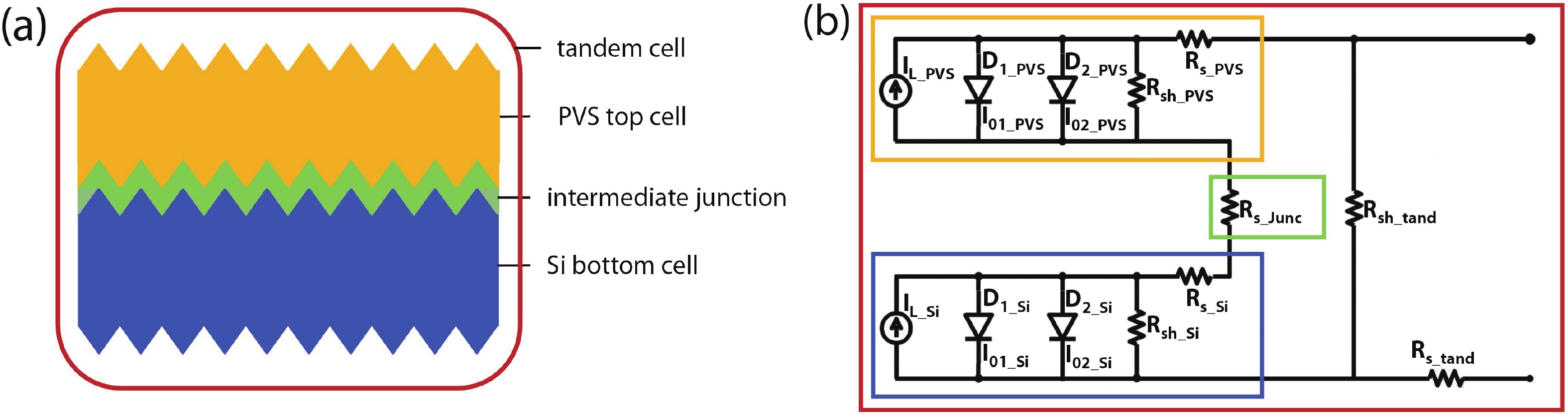
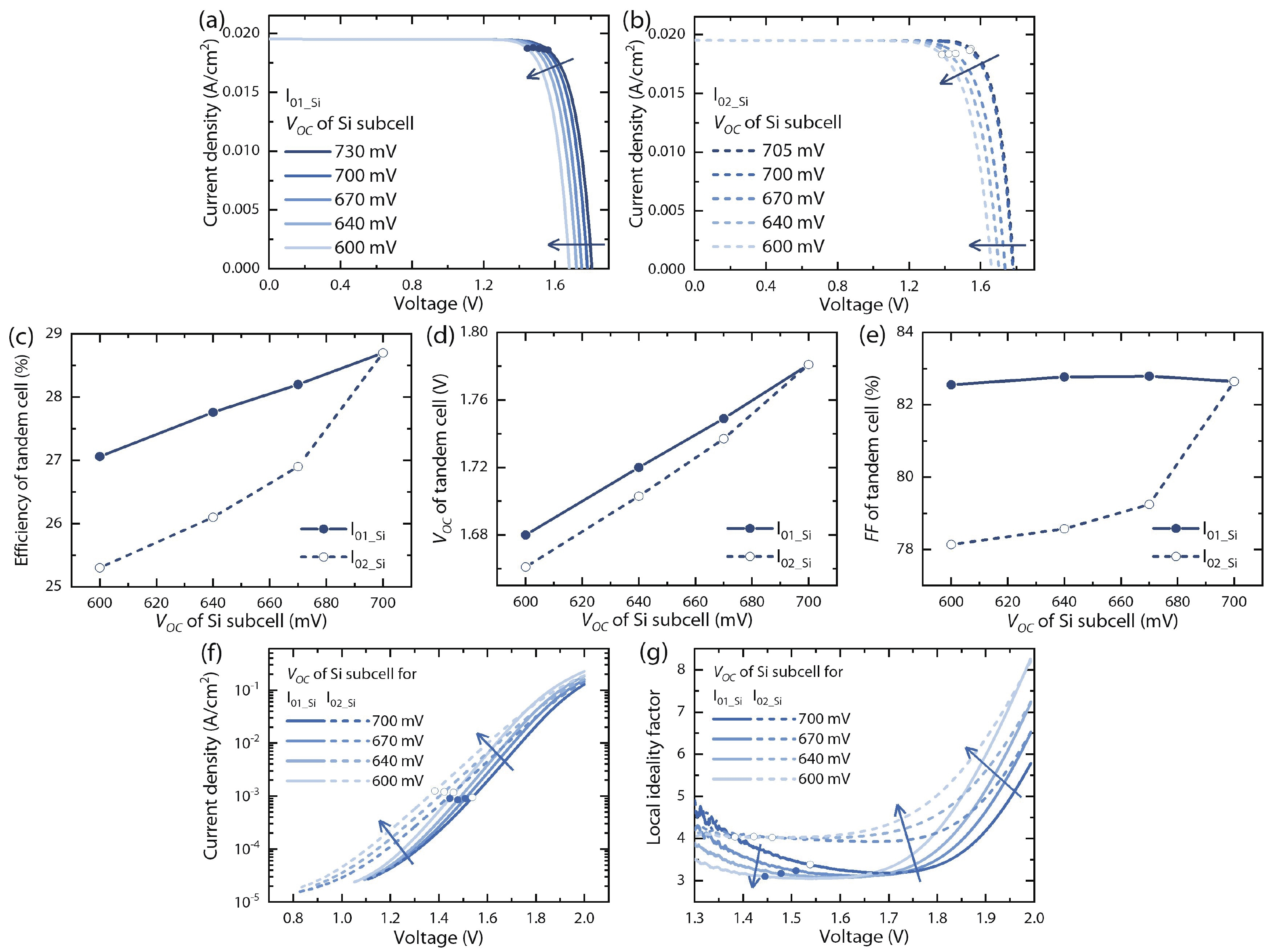
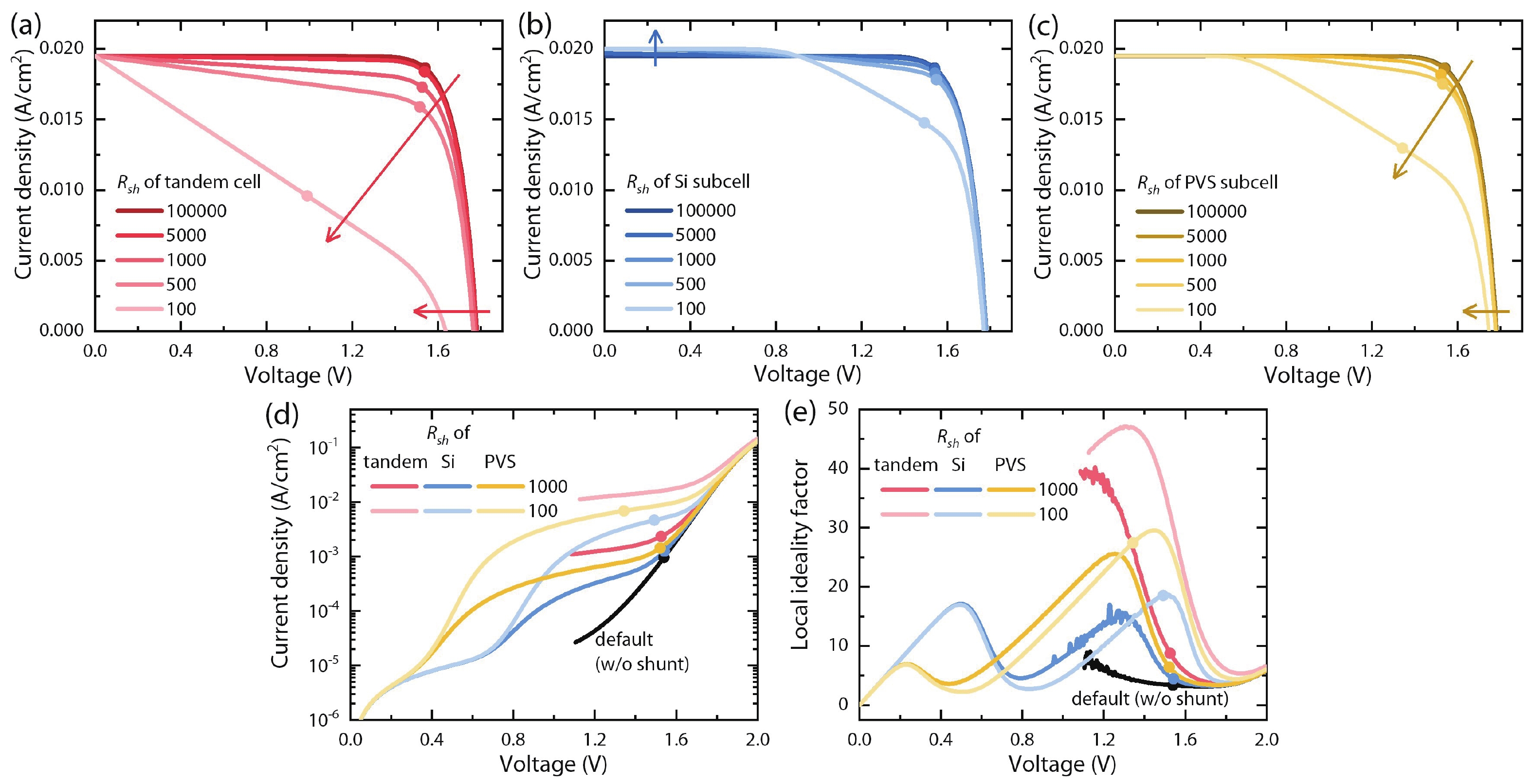
Bauer A, Hanisch J, Ahlswede E. An effective single solar cell equivalent circuit model for two or more solar cells connected in series. IEEE J Photovolt, 2014, 4(1), 340 doi: 10.1109/JPHOTOV.2013.2283056 |
| [13] |
Domínguez C, Antón I, Sala G. Multijunction solar cell model for translating I-V characteristics as a function of irradiance, spectrum, and cell temperature. Prog Photovolt, 2010, 18(4), 272 doi: doi.org/10.1002/pip.965 |
| [14] |
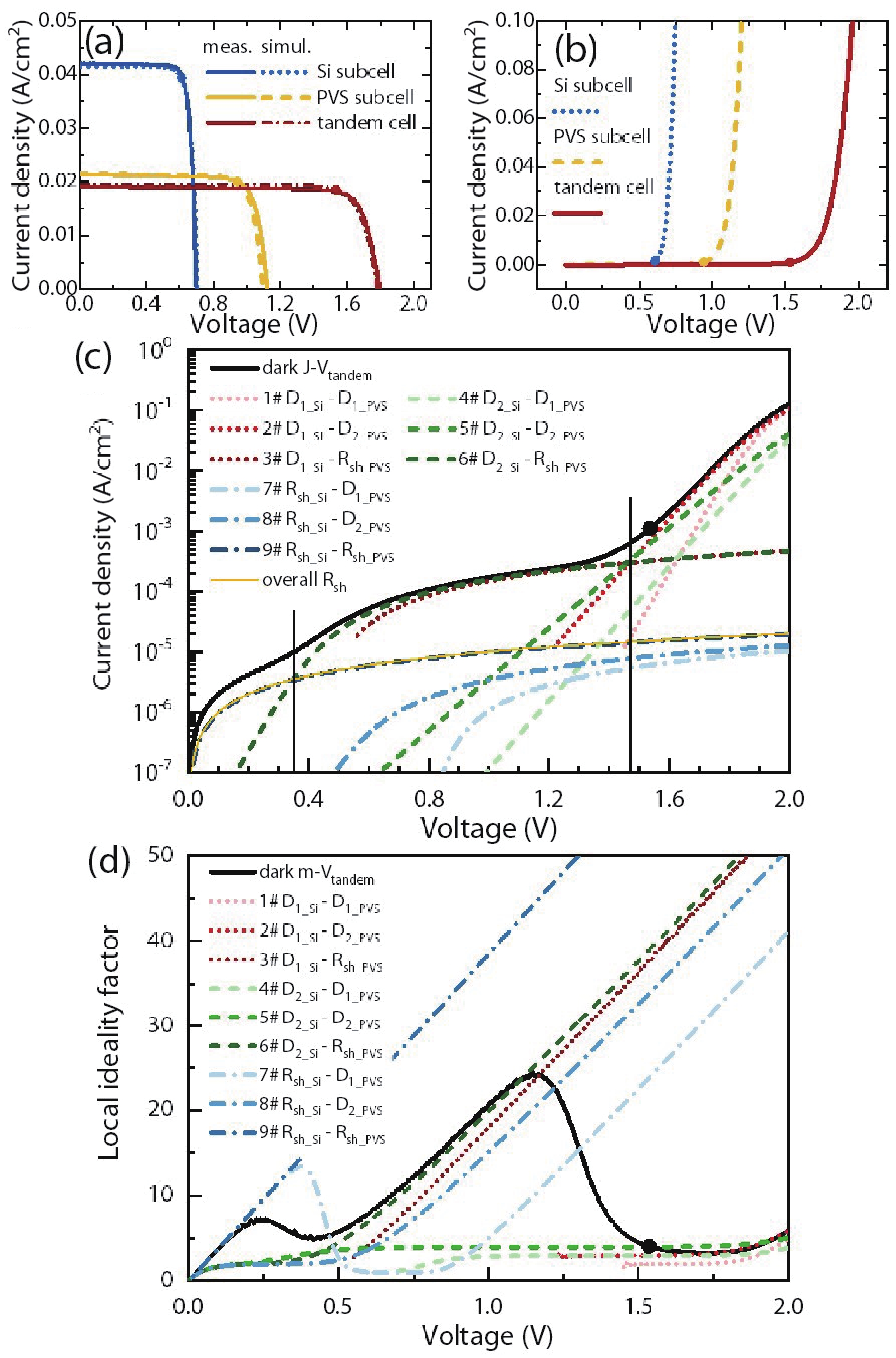
Lang F, Köhnen E, Warby J, et al. Revealing fundamental efficiency limits of monolithic perovskite/silicon tandem photovoltaics through subcell characterization. ACS Energy Lett, 2021, 6(11), 3982 doi: 10.1021/acsenergylett.1c01783 |
| [15] |
Agarwal Y, Das B, Dutta A J, et al. Numerical simulation of tunneling effect in high-efficiency perovskite/silicon tandem solar cell. 2020 47th IEEE Photovoltaic Specialists Conference (PVSC), 2021, 1318 doi: 10.1109/PVSC45281.2020.9300412 |
| [16] |
Blaga C, Christmann G, Boccard M, et al. Palliating the efficiency loss due to shunting in perovskite/silicon tandem solar cells through modifying the resistive properties of the recombination junction. Sustainable Energy Fuels, 2021, 5(7), 2036 doi: 10.1039/D1SE00030F |
| [17] |
Miyano K, Tripathi N, Yanagida M, et al. Lead halide perovskite photovoltaic as a model p–i–n diode. Acc Chem Res, 2016, 49, 303 doi: 10.1021/acs.accounts.5b00436 |
| [18] |
Velilla E, Cano J, Jimenez K, et al. Numerical analysis to determine reliable one-diode model parameters for perovskite solar cells. Energies, 2018, 11(8), 1963 doi: 10.3390/en11081963 |
| [19] |
Cappelletti M A, Casas G A, Cédola A P, et al. Study of the reverse saturation current and series resistance of p-p-n perovskite solar cells using the single and double-diode models. Superlattices Microstruct, 2018, 123, 338 doi: 10.1016/j.spmi.2018.09.023 |
| [20] |
Boccard M, Ballif C. Influence of the subcell properties on the fill factor of two-terminal perovskite–silicon tandem solar cells. ACS Energy Lett, 2020, 5(4), 1077 doi: 10.1021/acsenergylett.0c00156 |
| [21] |
Tockhorn P, Wagner P, Kegelmann L, et al. Three-terminal perovskite/silicon tandem solar cells with top and interdigitated rear contacts. ACS Appl Energy Mater, 2020, 3(2), 1381 doi: 10.1021/acsaem.9b01800 |
| [22] |
Green M A. Solar cells: operating principles, technology, and system applications. Englewood Cliffs, 1982
|
| [23] |
Sah C T, Noyce R N, Shockley W. Carrier generation and recombination in P-N junctions and P-N junction characteristics. Proc IRE, 1957, 45(9), 1228 doi: 10.1109/JRPROC.1957.278528 |
| [24] |
Henry C H, Logan R A, Merritt F R. The effect of surface recombination on current in Al xGa 1–xAs heterojunctions. J Appl Phys, 1978, 49(6), 3530 doi: 10.1063/1.325265 |
| [25] |
Fong K C, McIntosh K R, Blakers A W. Accurate series resistance measurement of solar cells. Prog Photovolt, 2013, 21(4), 490 doi: 10.1002/pip.1216 |
| [26] |
Lin Y R, Yang Z H, Liu Z K, et al. Dual-functional carbon-doped polysilicon films for passivating contact solar cells: Regulating physical contacts while promoting photoelectrical properties. Energy Environ Sci, 2021, 14, 6406 doi: 10.1039/D1EE02011K |
| [27] |
Ying Z Q, Yang X, Zheng J M, et al. Charge-transfer induced multifunctional BCP: Ag complexes for semi-transparent perovskite solar cells with a record fill factor of 80.1%. J Mater Chem A, 2021, 9(20), 12009 doi: 10.1039/D1TA01180D |
| [28] |
Ying Z Q, Yang Z H, Zheng J M, et al. Monolithic perovskite/black-silicon tandems based on tunnel oxide passivated contacts. Joule, 2022, 6, 2644 doi: 10.1016/j.joule.2022.09.006 |
| [29] |
Shou C H, Zheng J M, Han Q L, et al. Optimization of tunnel-junction for perovskite/tunnel oxide passivated contact (TOPCon) tandem solar cells. Phys Status Solidi A, 2021, 218, 2100562 doi: 10.1002/pssa.202100562 |
| [30] |
Green M A, Blakers A W, Osterwald C R. Characterization of high-efficiency silicon solar cells. J Appl Phys, 1985, 58(11), 4402 doi: 10.1063/1.336286 |
| [31] |
Saint-Cast P, Werner S, Greulich J, et al. Analysis of the losses of industrial-type PERC solar cells. Phys Status Solidi A, 2017, 214(3), 1600708 doi: 10.1002/pssa.201600708 |


 DownLoad:


 Yuheng Zeng:received his bachelor's and PhD degrees from Zhejiang University. He is a professor at Ningbo Institute of Materials Technology & Engineering (CAS). His research interests include crystalline silicon materials, silicon solar cells, and perovskite/silicon tandem solar cells. He has published more than 100 SCI papers
 Zhenhai Yang:received his master and PhD degree from Soochow University and the University of Nottingham (Ningbo), respectively. His research interests include the advanced optical designs, photoelectric models/simulations, structure designs, carrier transport processes, and the related mechanisms for TOPCon and perovskite-based single/tandem solar cells
 Jichun Ye:received his bachelor's and PhD degrees from University of Science and Technology of China and University of California Davis. He has more than 20 years of research and development experience in semiconductor devices, solar cells, and materials and has published more than 220 high-quality papers


