| [1] |
|
| [2] |
Dietl T, Ohno H, Matsukura F, et al. Zener model description of ferromagnetism in zinc-blende magnetic semiconductors. Science, 2000, 287, 1019 doi: 10.1126/science.287.5455.1019 |
| [3] |
Chiba D, Sawicki M, Nishitani Y, et al. Magnetization vector manipulation by electric fields. Nature, 2008, 455, 515 doi: 10.1038/nature07318 |
| [4] |
Jungwirth T, Wunderlich J, Novák V, et al. Spin-dependent phenomena and device concepts explored in (Ga, Mn)As. Rev Mod Phys, 2014, 86, 855 doi: 10.1103/RevModPhys.86.855 |
| [5] |
Dietl T, Ohno H. Dilute ferromagnetic semiconductors: Physics and spintronic structures. Rev Mod Phys, 2014, 86, 187 doi: 10.1103/RevModPhys.86.187 |
| [6] |
Ohno H, Munekata H, Penney T, et al. Magnetotransport properties of p-type (In, Mn)As diluted magnetic III-V semiconductors. Phys Rev Lett, 1992, 68, 2664 doi: 10.1103/PhysRevLett.68.2664 |
| [7] |
Koshihara S, Oiwa A, Hirasawa M, et al. Ferromagnetic order induced by photogenerated carriers in magnetic III-V semiconductor heterostructures of (In, Mn)As/GaSb. Phys Rev Lett, 1997, 78, 4617 doi: 10.1103/PhysRevLett.78.4617 |
| [8] |
Akai H. Ferromagnetism and its stability in the diluted magnetic semiconductor (In, Mn)As. Phys Rev Lett, 1998, 81, 3002 doi: 10.1103/PhysRevLett.81.3002 |
| [9] |
Oiwa A, Endo A, Katsumoto S, et al. Magnetic and transport properties of the ferromagnetic semiconductor heterostructures (In, Mn)As/(Ga, Al)Sb. Phys Rev B, 1999, 59, 5826 doi: 10.1103/PhysRevB.59.5826 |
| [10] |
Schallenberg T, Munekata H. Preparation of ferromagnetic (In, Mn)As with a high Curie temperature of 90K. Appl Phys Lett, 2006, 89, 042507 doi: 10.1063/1.2236210 |
| [11] |
Ohno H, Shen A, Matsukura F, et al. (Ga, Mn)As: A new diluted magnetic semiconductor based on GaAs. Appl Phys Lett, 1996, 69, 363 doi: 10.1063/1.118061 |
| [12] |
Matsukura F, Ohno H, Shen A, et al. Transport properties and origin of ferromagnetism in (Ga, Mn)As. Phys Rev B, 1998, 57, R2037 doi: 10.1103/PhysRevB.57.R2037 |
| [13] |
Chen L, Yang X, Yang F H, et al. Enhancing the curie temperature of ferromagnetic semiconductor (Ga, Mn)As to 200 K via nanostructure engineering. Nano Lett, 2011, 11, 2584 doi: 10.1021/nl201187m |
| [14] |
Wang H L, Ma J L, Zhao J H. Giant modulation of magnetism in (Ga, Mn)As ultrathin films via electric field. J Semicond, 2019, 40, 092501 doi: 10.1088/1674-4926/40/9/092501 |
| [15] |
Wang H L, Ma J L, Wei Q Q, et al. Mn doping effects on the gate-tunable transport properties of Cd 3As 2 films epitaxied on GaAs. J Semicond, 2020, 41, 072903 doi: 10.1088/1674-4926/41/7/072903 |
| [16] |
Tu N T, Hai P N, Anh L D, et al. (Ga, Fe)Sb: A p-type ferromagnetic semiconductor. Appl Phys Lett, 2014, 105, 132402 doi: 10.1063/1.4896539 |
| [17] |
Tu N T, Hai P N, Anh L D, et al. Magnetic properties and intrinsic ferromagnetism in (Ga, Fe)Sb ferromagnetic semiconductors. Phys Rev B, 2015, 92, 144403 doi: 10.1103/PhysRevB.92.144403 |
| [18] |
Tu N T, Hai P N, Anh L D, et al. High-temperature ferromagnetism in heavily Fe-doped ferromagnetic semiconductor (Ga, Fe)Sb. Appl Phys Lett, 2016, 108, 192401 doi: 10.1063/1.4948692 |
| [19] |
Goel S, Anh L D, Ohya S, et al. Ferromagnetic resonance and control of magnetic anisotropy by epitaxial strain in the ferromagnetic semiconductor (Ga 0.8, Fe 0.2)Sb at room temperature. Phys Rev B, 2019, 99, 014431 doi: 10.1103/PhysRevB.99.014431 |
| [20] |
Goel S, Anh L D, Ohya S, et al. In-plane to perpendicular magnetic anisotropy switching in heavily-Fe-doped ferromagnetic semiconductor (Ga, Fe)Sb with high Curie temperature. Phys Rev Materials , 2019, 084417 doi: 10.1103/PhysRevMaterials.3.084417 |
| [21] |
Tu N T, Hai P N, Anh L D, et al. High-temperature ferromagnetism in new n-type Fe-doped ferromagnetic semiconductor (In, Fe)Sb. Appl Phys Express, 2018, 11, 063005 doi: 10.7567/APEX.11.063005 |
| [22] |
Nguyen T T, Pham N, Le D, et al. Electrical control of ferromagnetism in the n-type ferromagnetic semiconductor (In, Fe)Sb with high Curie temperature. Appl Phys Lett, 2018, 112, 122409 doi: 10.1063/1.5022828 |
| [23] |
Nguyen T T, Pham N H, Le D A, et al. Heavily Fe-doped n-type ferromagnetic semiconductor (In, Fe)Sb with high Curie temperature and large magnetic anisotropy. 2019 Compound Semiconductor Week (CSW), Nara, Japan, 2019, 1 doi: 10.1109/ICIPRM.2019.8819236 |
| [24] |
Sakamoto S, Tu N T, Takeda Y, et al. Electronic structure of the high-T C ferromagnetic semiconductor (Ga, Fe)Sb: X-ray magnetic circular dichroism and resonance photoemission spectroscopy studies. Phys Rev B, 2019, 100, 035204 doi: 10.1103/PhysRevB.100.035204 |
| [25] |
Sriharsha K, Anh L D, Tu N T, et al. Magneto-optical spectra and the presence of an impurity band in p-type ferromagnetic semiconductor (Ga, Fe)Sb with high Curie temperature. APL Mater, 2019, 7, 021105 doi: 10.1063/1.5083175 |
| [26] |
Tanaka M. Recent progress in ferromagnetic semiconductors and spintronics devices. Jpn J Appl Phys, 2021, 60, 010101 doi: 10.35848/1347-4065/abcadc |
| [27] |
Stefanowicz W, Śliwa C, Aleshkevych P, et al. Magnetic anisotropy of epitaxial (Ga, Mn)As on (113)A GaAs. Phys Rev B, 2010, 81, 155203 doi: 10.1103/PhysRevB.81.155203 |


 Zhi Deng obtained his B.E. degree from Center of Materials Science and Optoelectronics Engineering in 2020 at University of Chinese Academy of Sciences. He then joined the State Key Laboratory of Superlattices and Microstructures under the supervision of Prof. Jianhua Zhao. His research focuses on Fe-based Ⅲ−Ⅴ magnetic semiconductors.
 Hailong Wang received his B.Sc. degree from the School of Physics of Peking University in 2009, and a PhD degree from the University of Chinese Academy of Sciences in 2014. From 2014 to 2016, he was a postdoc at the Institute of Physics in Chinese Academy of Sciences, and then worked in the Institute of Semiconductors in Chinese Academy of Sciences. His current interests include Ⅲ−Ⅴ magnetic semiconductors, semiconductor two-dimensional electron gas and magnetic metal/semiconductor heterostructures.
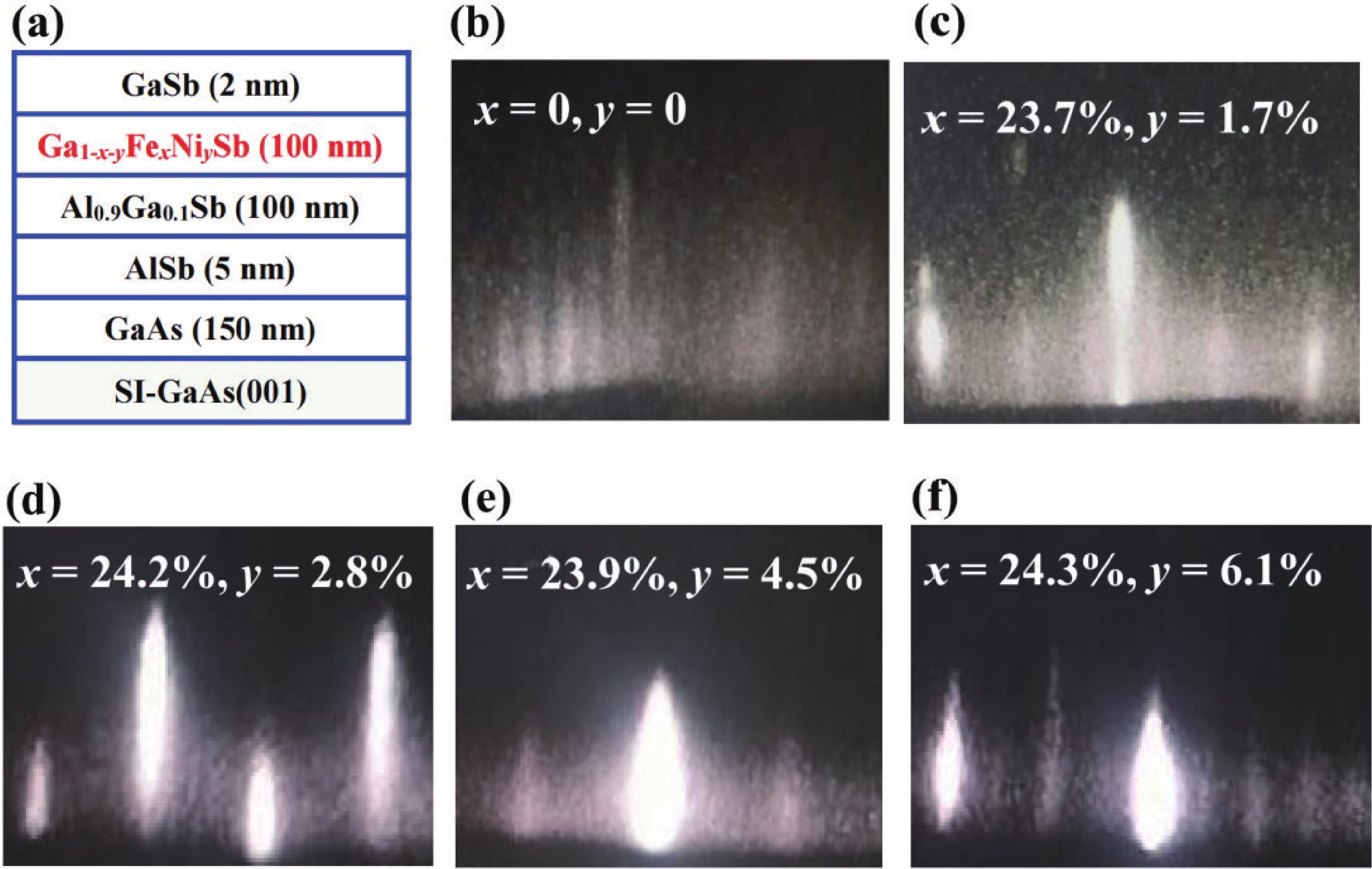
 DownLoad: