J. Semicond. > 2024, Volume 45 > Issue 2 > 022701

ARTICLES

An advanced theoretical approach to study super-multiperiod superlattices: theory vs experiments

Alexander Sergeevich Dashkov1, 2, , Semyon Andreevich Khakhulin1, Dmitrii Alekseevich Shapran1, Gennadii Fedorovich Glinskii1, Nikita Andreevich Kostromin1, 3, Alexander Leonidovich Vasiliev4, 5, Sergey Nikolayevich Yakunin4, 5, Oleg Sergeevich Komkov1, Evgeniy Viktorovich Pirogov2, Maxim Sergeevich Sobolev2, Leonid Ivanovich Goray1, 2, 6, 7 and Alexei Dmitrievich Bouravleuv1, 6, 7, 8

+ Author Affiliations

 Corresponding author: Alexander Sergeevich Dashkov, dashkov.Alexander.OM@gmail.com

DOI: 10.1088/1674-4926/45/2/022701

PDF

Turn off MathJax

Abstract: A new theoretical method to study super-multiperiod superlattices has been developed. The method combines the precision of the 8-band kp-method with the flexibility of the shooting method and the Monte Carlo approach. This method was applied to examine the finest quality samples of super-multiperiod Al0.3Ga0.7As/GaAs superlattices grown by molecular beam epitaxy. The express photoreflectance spectroscopy method was utilized to validate the proposed theoretical method. For the first time, the accurate theoretical analysis of the energy band diagram of super-multiperiod superlattices with experimental verification has been conducted. The proposed approach highly accurately determines transition peak positions and enables the calculation of the energy band diagram, transition energies, relaxation rates, and gain estimation. It has achieved a remarkably low 5% error compared to the commonly used method, which typically results in a 25% error, and allowed to recover the superlattice parameters. The retrieved intrinsic parameters of the samples aligned with XRD data and growth parameters. The proposed method also accurately predicted the escape of the second energy level for quantum well thicknesses less than 5 nm, as was observed in photoreflectance experiments. The new designs of THz light-emitting devices operating at room temperature were suggested by the developed method.

Key words: super-multiperiod superlatticephotoreflectance spectroscopyKane modelkp-methodenergy band diagramlight amplifiers

Semiconductor superlattices (SLs) are semiconductor materials that incorporate a one-dimensional periodic potential with a period larger than the crystal lattice[1]. In these materials, the motion of charge carriers is confined along one of the dimensions, resulting in unique quantum properties and modification of the band structure of the host semiconductors. Even several decades after the first study of SL was published, scientific groups still discover new applications[2, 3] and curious properties[4, 5] of these quantum structures.

One of their most promising applications is the creation of THz-emitting devices. The THz radiation has a variety of essential applications in medicine, astronomy, and telecommunications[6, 7], which indicates the need to produce new cutting-edge tunable THz sources operating at room temperature. Multiperiod SLs are the prime candidates for this job because they have all the components required for light amplification and their designs seems to be simpler and more reliable, than designs of quantum cascade lasers (QCLs)[8, 9]. The ongoing simplification of designs of QCLs towards the SLs[10, 11] confirms this conclusion.

Experimental studies and fabrication of SLs have become possible in the last several decades due to significant progress in growth technologies. The most valuable contribution to this research field was made by molecular beam epitaxy (MBE), which brought to life more and more devices with ultra-thin layers. Moreover, a new type of SL, super-multiperiod (SMP) structures, i.e., SLs with a number of layers from several hundred up to few thousands have been recently implemented by MBE[9, 1216].

In both cases (ordinary or SMP SLs), researchers need to solve the Schrödinger equation with the given periodic electronic potential. The introduction of such potential leads to the transformation of the initial electronic Bloch states and minibands formation. Currently, there are plenty of numerical methods to get this information qualitatively and quantitatively. But they all incorporate a variety of assumptions, limitations, and approximations. For instance, kp-methods consider states in the vicinity of the selected point of the Brillouin zone, whereas the density functional theory calculations require a complex and intense computation procedure[17]. At the same time, all these methods are the most appropriate ways to tackle the problem of determination of the electronic properties of SL. However, in more intriguing cases, the theory is yet to be solidified, e.g., SMP SLs under external electric fields. One of the vivid examples of this fact is the problem of predicted low gain values in SLs[11]. It was suggested, that in similar SL structures, the gain is strongly affected by elastic scattering for a higher temperature. To the best of our knowledge, such comprehensive investigations, which considers combination of both experimental and theoretical approaches, have not been conducted yet.

In this work, a new theoretical approach for the modelling of SMP SL parameters is developed. Our method combines theoretical and numerical models, including 8 band kp- and shooting methods, as well as Monte Carlo (MC) simulations. The developed approach was proved by the study of the properties of AlxGa1-xAs/GaAs SMP SL samples of the finest quality obtained by MBE. These samples were also examined by the express method of photoreflectance spectroscopy (PRS) and high-resolution transmission electron microscopy (HR ТЕМ). Conducted research establishes the accuracy, applicability, and versatility of the developed approach.

The AlxGa1-xAs/GaAs SMP SLs of high quality were grown on one-sided semi-insulating GaAs (100) substrates using the Riber 49 MBE setup. The reflection high-energy electron diffraction system was used to control the growth processes in situ. The thickness of the GaAs layers in the synthesized SMP SL structures differs across the samples, while the barrier AlxGa1-xAs thickness remains constant. The Al mole fraction x in the barrier layers was equal to 30%. The grown SMP SL structures were doped identically in barriers and wells with silicon as an n-type dopant. All samples had the same concentrations of n-type donor dopant (n = 1016 cm−3). Table 1 contains all the essential parameters for the samples.

Table 1.  Parameters of the AlxGa1-xAs/GaAs superlattices samples under study.
No. Al(%) Doping level
(сm−3)
Number of periods
(counts)
Well thickness (nm) Barrier thickness (nm) Designed period
(nm)
Period from XRD
(nm)
1 30 1016 100 10 2 12 12.0
2 30 1016 100 7 2 9 8.99
DownLoad: CSV  | Show Table

Obtained samples exhibit the excellent quality of the SMP SLs which was confirmed by different methods. The detailed metrology of the grown doped and undoped SMP SL AlxGa1-xAs/GaAs structures with period numbers of 100–400 was carried out by high-resolution X-ray reflectometric (HRXRR), deep X-ray reflectometric (DXRR) and high-resolution diffractometric (HRXRD) studies, in particular, using a synchrotron radiation source[12, 13, 15, 16]. The difference in the thicknesses of the grown layers, estimated by three methods and over the entire depth of the optimized SL structures, was no more than 0.5–2.0 percent, the interface root mean square (RMS) roughness was a few Å, and the composition inaccuracy was ~0.5 atomic percent. The high sharpness of SLs’ interfaces was also demonstrated by high-resolution transmission electron microscopy (HR TEM) (see Fig. A1 and Supplementary materials)[13, 18].

One of the main methods used for precise energy spectrum retrieving was PRS[19, 20]. PRS is the non-contact, non-destructive, and highly sensitive express method for diagnosing nanostructures. It allowed us to determine the energies of interband optical transitions in nanostructures not only at low[21], but also at room temperature ranges[22, 23]. One can also obtain information about higher-order optical transitions in different nanostructures[24, 25], including type-Ⅱ SLs[26]. The high quality of the grown samples makes this method applicable for the precise examination of optical properties of SMP SLs even at room temperatures. PRS is based on the application of both the probe laser beam, which varies in a wide energy range, and the periodic modulated laser beam. The electron−hole pairs photoinduced as a result of laser exposure are separated by the near-surface built-in electric field. At the frequency of the periodic laser perturbation, a change in the reflectance coefficient is synchronously detected, which underlies the recorded signal[19]. During the study of low-dimensional semiconductor structures, the formation of a signal can occur due to a change in the position of quantum-dimensional levels under the action of a change in the built-in electric field due to the Stark effect[27]. In case of SLs, the quantum-dimensional levels can be transformed into several energy minibands of finite width. Therefore, singularities in the photoreflectance (PR) spectra can be observed at energies corresponding to the maximum and minimum energies of possible transitions between minibands (near the Г and П points of the Brillouin zone of the SL)[2830].

The PR spectra were measured using an experimental setup assembled on the basis of an IKS-31 diffraction spectrometer. The source of modulating radiation was a highly stable SSP-DHS-405 violet laser with an operating wavelength of λ = 405 nm. The laser beam was aimed at the exact area of the sample where the spectrometer's monochromatic light was directed to. Modulation signal was recorded using a silicon photodiode, a preamplifier, and a lock-in amplifier (SR830, Stanford Research). The measured PR spectra represent a series of differential signals, the inflection points of which determine the energy values of optical transitions[19]. To get accurate energy values and characterize spectral features, PR spectra were transformed using the Kramers–Kronig relations (Kramers–Kronig method, KKM)[31]. The Appendix B provides a detailed explanation of this transformation. The extrema of transformed signals determine the precise energy values of the observed optical transitions.

The presented SMP SL structures in Table 1 were initially designed for the light amplifiers’ implementation. The geometry of these SLs was inspired by the structures proposed in Ref. [8] and underwent a few modifications for output characteristics improvement, including estimated gain[9]. When the electric field is applied to such SLs, light amplification becomes possible due to the emergence of optical intersubband transitions. Since these transitions occur between energy minibands of SL, their relative position, i.e., the emitting wavelength, can be tuned with the applied field. In this case, all output characteristics of the SLs depend on their parameters (layer thicknesses, composition, and doping concentrations). For instance, thinner Al0.3Ga0.7As barriers maintain higher dipole matrix element values for optical transitions, resulting in higher gain values. Such qualitative considerations provide a general idea of the structure design but do not define it completely. Therefore, to fully define the structure, i.e., to choose structure parameters suitable for the task, it is necessary to carry out numerical simulations of the SL energy spectrum.

The initial designing process was based entirely on the results of the classical shooting method (CSM) simulations[32]. Applied CSM utilizes the approximation of the single-band kp-model, an easily-implementable computation scheme which showed a good agreement with experimental results for a single quantum well, multiple quantum well structures, and ordinary SLs[33, 3437]. This method has been also selected because it is frequently utilized to address similar QCL simulation tasks[10, 38]. CSM retrieves the electronic eigenstates, which define the electronic energy spectrum for a given SL periodic potential. A boundary value problem for the Schrödinger equation in CSM is reduced to the Cauchy problem, i.e., an initial value problem[32]. The electronic eigenstates are determined by 'shooting' solutions from one boundary condition with different initial conditions until the other boundary condition is met. Once the eigenvalues are found, one can employ a transfer matrix approach to retrieve wavefunctions via the propagation procedure. The transition energies are defined as the difference between the values of the corresponding eigenenergies (minibands' boundaries). The electronic energetic spectrum is then utilized in a stochastic MC approach to gather information about the kinetics of the SLs, such as transition rates and gain estimations. The Fermi golden rule is applied to calculate the scattering rates used in MC, including phonon and impurity scattering rates. For example, to calculate the impurity scattering rate the following formula can be employed:

Wik,j=m||je44πϵ23π0Fij(q)dθq2,
(1)

where q(θ)=|kk|,Fij=dznD(z)[ψi(z)ψj(z)exp(q|zz|)dz]2, k,k are plane wave vectors, θ is the angle between k, k, V is impurity potential, nD is doping sheet density for the considered layer, i, j are indexes of eigenenergy levels of SL between which the scattering occurs, m||j is in-plane electron effective mass for the j-th energy level, e is the elementary charge, the dielectric permittivity ϵ=ϵ0ϵr,0, ϵ0 is the vacuum permittivity, ϵr,0 is the static dielectric constant. For scattering on longitudinal optical (LO) phonon:

Wik,j=m||je2ωLO(ϵ1r,ϵ1r,0)(Nph+12+12)8π22ϵ02π0Fijdθ,
(2)

where q=|kk|,Fij=πqdzdznD(z)ψj(z)ψj(z)ψi(z)ψi(z)exp(q|zz|),ωLO is the LO phonon frequency at Q=0,Q is the phonon wave vector, Nph is the mode independent phonon occupation number, ϵr, is the high frequency dielectric constant.

To estimate gain based on dipole matrix element D and doping concentrating ne, the following formula, obtained from two level model was used[32]:

αg=4πωe2necnωγD2(E21ω)2+γ2tanh(E212kT),
(3)

where γ=τ11+τ12, D is the dipole matrix element, E21 is the energy of transition, ω is the angular frequency of radiation, nω is the refractive index of the structure, T is the electron temperature, c is the vacuum speed of light, τi is the lifetime of the level i. The influence of the coherence of the electron transport[39] was considered implicitly in the MC approach via collisional broadening in the γ parameter[40]. Usually, a depolarization shift is also taken into account in classical designs of THz QCLs[41]. However, this shift was neglected in that case due to several reasons. First, in case of SMP SLs with the considered doping levels and slightly different lasing scheme (compared to QCLs), further investigation is still required to analyze the impact of such depolarization shift. Moreover, all the computations were performed for room temperature and biases of approximately 50 kV/cm. There is experimental evidence that in such cases, the depolarization effect influences the shape of the gain curve, but the shift becomes less pronounced[42, 43]. Also, the figure of merit FM was utilized to take into account both dipole matrix element and population inversion between upper u and lower l states[44]:

FM=D2ulτeff=Dulτu(1τlτul),
(4)

where Dul is the dipole matrix element for transition between upper and lower levels, τul is the inverse transition rate between upper and lower levels.

During the design phase, we varied the thicknesses of all the layers and layer composition to maximize both the figure of merit and gain estimation while preserving the emitting wavelength in the THz range. In order to check the calculated design, a series of SMP SL Al0.3Ga0.7As/GaAs structures were grown (Table 1). SMP SL structures had sharp interfaces, their thicknesses and composition deviations were minimal (see Fig. A1 and Supplementary materials). The creation of such high-quality SMP SLs with required layer thicknesses and acceptable interface widths became possible due to laboratory and synchrotron studies[12], as it was mentioned in the previous section.

The optical properties of the samples were examined by PRS to determine the electronic energy spectrum. The PR examination is a suitable verification tool because the electronic energy spectrum and the optical output features of the structures are closely interconnected. Therefore, for all the grown SMP SL structures, PR spectra were measured and transformed according to the method described in the previous section and Supplementary materials. The data obtained were compared with CSM results. For instance, the e1−hh1 transition energy, i.e., the difference between the first electronic (e1) and the first heavy hole (hh1) energy levels, was compared with the position of the first peak in the transformed spectrum.

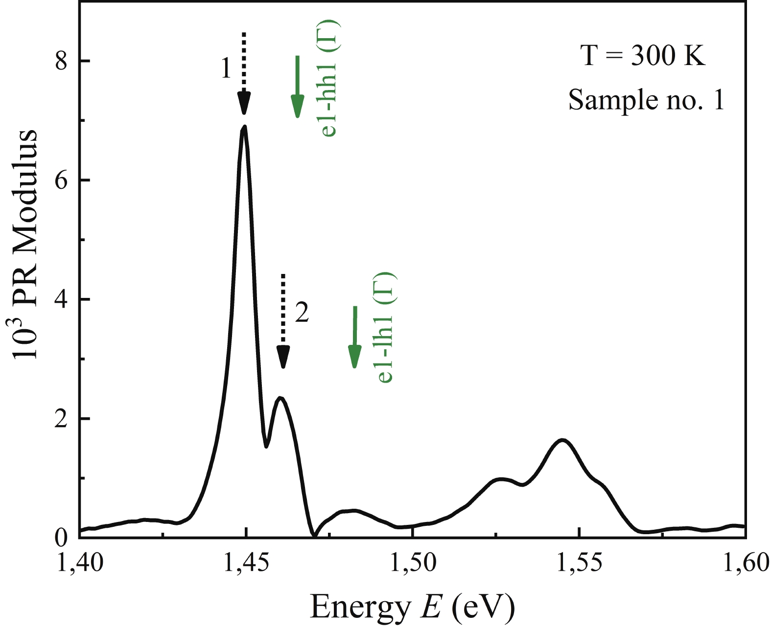
We anticipated only minor deviations between experimental and simulated values since CSM is widely applied in similar QCL design tasks[32]. However, the PR analysis (Fig. 1) of sample no. 1 showed a significant deviation from the expected band structure: simulated energy values (green arrows in Fig. 1) and experimental values (black dotted arrows in Fig. 1) differed for e1−hh1 and e1−lh1 transitions by 15 meV and 23 meV, respectively. That results in a total error of about 25% and makes CSM inapplicable for the proper and complete electronic energy spectra analysis of SMP SLs.

Fig. 1.  (Color online) The transformed PR spectrum of sample no. 1 measured at T = 300 K. Black dotted arrows indicate the experimental transition energy peaks and green solid arrows indicate the transition energy positions computed by CSM.

As CSM was not suitable for the analysis of the transformed PR spectrum, we had to find an alternative simulation approach. The first idea was to test more advanced purely numerical methods: the finite elements method (FEM), which numerically solves the Schrödinger equation for an infinite SL on the specified grid[32]; the transfer matrix approach with the Airy functions and immense modifications of the shooting method, which also provides the numerical procedure to obtain the minibands position of SL[32, 37]. We reduced the error to 10%, but the accuracy of these methods was still insufficient for an unambiguous analysis of experimental data. Therefore, we changed our simulation approach to a more elaborate one.

It is well known that the theoretical study of semiconductor heterostructures and SLs can be done in various ways: the empirical pseudopotential method (EPM)[33, 4548], the tight binding (TB) method[33, 48], and the kp-method[3336]. All of the mentioned methods allow to simulate SLs with a large number of periods (here, SMP SLs). However, there are few works only[8, 11] that include the experimental study of such SLs combined with theoretical and numerical analysis. Some of these methods even assume that the SL under consideration is infinite[3336, 4652]. This is also an approximation to be verified with the experimental data. Taking into account all of these facts, it was not clear which method to choose. The EPM has an advantage over TB, since EPM requires fewer adjustable parameters and a suitable basis for the solving of the Schrödinger equation can always be chosen. The EPM makes it possible to obtain results those are in good agreement with the experiment[33, 45, 46], since it can account any number of bands contributing to the formation of energy states. However, such many band EPM considerations impose additional computational requirements even for the structures whose dimensions are just a few nanometers. Although there are ways to get around these difficulties[33], the computers used have not allowed one to study SMP SLs with a supercell of more than ~2–3 nm in size by this method. The kp-method is suitable for investigation of nanostructures larger than a few nanometers, including SMP SLs, as it was demonstrated in Refs. [36, 50]. This method is also among the most appropriate methods for analyzing experimental data. The complexity of the kp-method increases with the number of bands considered in the calculation[3436, 53]. The initial simulation approach included only an approximation of the single band kp-method, which probably was the reason for poor accuracy. Thus, we selected the below-described 8-band kp-method, also known as the Kane model, for the appropriate theoretical study of the SMP SLs.

The 8-band Kane model was previously used to calculate the energy spectrum and interband matrix elements of similar heterostructures and SLs[49]. One of the key advantages of the Kane model is that it allows to consider the nonparabolicity of the charge carriers' dispersion law. Another bonus is the insignificant computational burden of the model, even in our case of SMP SLs[35]. The model can be formulated as an eigenenergy problem for the Schrödinger equation with the following Hamiltonian:

Hkk(K)=(H(Γc6)kk(K)HΓc6Γv8kk(K)HΓc6Γv7kk(K)[HΓc6Γv8kk(K)]H(Γv8)kk(K)HΓv8Γv7kk(K)[HΓc6Γv7kk(K)][HΓv8Γv7kk(K)]H(Γv7)kk(K)).
(5)

According to Refs. [35, 49], this Hamiltonian matrix includes the effective Hamiltonians Hαα'kk'(K) , where k,k are the wave vector of an electron in the Brillouin zone of the crystal, α,α are the indexes of the considered bands (Γc6, Γv8 and Γv7 are the centers of the Brillouin zone of a bulk crystal for the conduction, valence, and spin-split bands, respectively, with spin momentum projections Γc6(c=±1/2), Γv8(v=±3/2,±1/2) and Γv7(v=±1/2), K is the wave vector of an electron in the Brillouin zone of SL. The main diagonal elements are the one-band effective Hamiltonians, and the off-diagonal elements describe the effects of the interband kp-interaction. Both types of Hamiltonians include the difference in the interband parameters of the materials when passing through the interface. When solving this problem, one can prevent false solutions in the multiband model by the k—representation method since the considered region of k—space can be limited based on the estimated width of the wave functions compared to the size of the Brillouin zone.

The primary method to solve the Schrödinger equation involved a periodical continuation of a single quantum well[35, 51, 52]. The periodicity condition leads to the fact that the wave vector k of an electron in a crystal becomes discrete, and the Schrödinger equation itself turns into a system of algebraic equations

α,kHααkk'(K)Fαk',l(K)=El(K)Fαk,l(K),
(6)

where Fαk,l(K)—the envelope wave function of an electron in the k-representation, l is the number of the band in the SL band structure. The components of the eigencolumns of the Hamiltonian Fαk,l(K) determine the contribution of the states |α,k of the reference crystal corresponding to the bands to the superlattice state |l,k.

To interpret the experimental data presented in Fig. 1, the calculation of the energy spectrum of charge carriers by Eq. (6) is not enough, since the experimental data reflect only the optical transition probabilities. The optical transition probabilities can be obtained from analyses of interband matrix elements, which are calculated with the following formula (neglecting the kp-interaction of electrons and holes):

Pll(K)=c,vkFΓc6l,k(K)PcvFΓv8,7k,l(K),
(7)

where Pcv is the matrix element of the momentum operator. For transitions of charge carriers from the valence band Γv8 to the conduction band Γc6, Pcv=Γc6|ˆP|Γv8. For transitions from the spin-split band Γv7 to the conduction band Γc6 Pcvso=Γc6|ˆP|Γv7, its projections have the form

Pxcv=P(i600i36i3600i6),Pycv=P(16001361360016),Pzcv=P(0i360000i360),
Pxcvso=P(0i3i30),Pycvso=P(0i3i30),Pzcvso=P(i300i3),
(8)

where P=Γ1|ˆpx|Γx15=Γ1|ˆpy|Γy15=Γ1|ˆpz|Γz15. Since the structures under study were grown in the direction [001], the projection of the matrix element onto the z axis did not contribute. It is important to note that the band anticrossing effects take place in the band structure for the hole states of the superlattice in the Kz direction. This leads to a sharp change in the selection rules for the optical matrix element Pll(K) when passing through the Kz point corresponding to the "anticrossing" of terms.

Table 2.  The band structure parameters used in the Kane model calculations at T = 300 K.
Parameter Material
GaAs AlAs AlxGa1xAs
a (Å) 5.6532 5 5.6611 aAlAsx+aGaAs(1x)
E(Γ)g(eV) 1.422 3.003 EAlAsx+EGaAs(1x)+(0.127+1.310x)(1x)
Δso(eV) 0.341 0.28 ΔAlAsx+ΔGaAs(1x)
me(Γ) 0.067 0.124
γL1 6.98 3.76
γL2 2.06 0.82
γL3 2.93 1.42
EP(eV) 28.8 21.1 EPAlAsx+EPGaAs(1x)
DownLoad: CSV  | Show Table

For the energy spectrum of charge carriers and interband matrix elements calculations the parameters of initial materials from Table 2 were used[54]. The Kane parameters required for the calculation were determined through the constants presented in Table 2 as follows:

γKc=γLcEp3[2E(Γ)g1E(Γ)g+Δso],γLc=1me(Γ),
γK1=γL1Ep3E(Γ)g,γK2=γL2Ep6E(Γ)g,γK3=γL3Ep6E(Γ)g,
γKiAlxGa1xAs=γKiAlAsx+γKiGaAs(1x),
Ep=2P2m0,
(9)

where m0 is the electron mass.

The band offset parameters were obtained from Ref. [50] and corresponded to the following relationship ΔEc/ΔEv=0.67/0.33. The band offset of spin-split bands was defined as ΔESO=ΔEv+(ΔGaAsSOΔAlxGa1xAsSO). It was also assumed that neglected deformation effects are insignificant since the relative difference between the constant lattices of the well and barrier materials is |ϵ|=0.097%. Therefore, the lattice period in the superlattice was taken as the AlxGa1-xAs period. We computed the transition energies for considered SMP SL structures using the above-described formulae. The resulting values are demonstrated in Table 3 and they were used for further PR spectra analysis.

Table 3.  Values of the optical transition energies (eV) calculated with the Kane model.
Transition type Point in k-space
Sample no. 1 Sample no. 2
Г П Г П
e1−hh1 1.449 1.466 1.486 1.516
e1−lh1 1.454 1.485 1.497 1.549
e2−hh2 1.591 1.529 1.763 1.647
e2−lh2 1.655 1.556 1.876 1.691
e3−hh3 1.662 1.779
e3−lh3 1.729 1.895
DownLoad: CSV  | Show Table
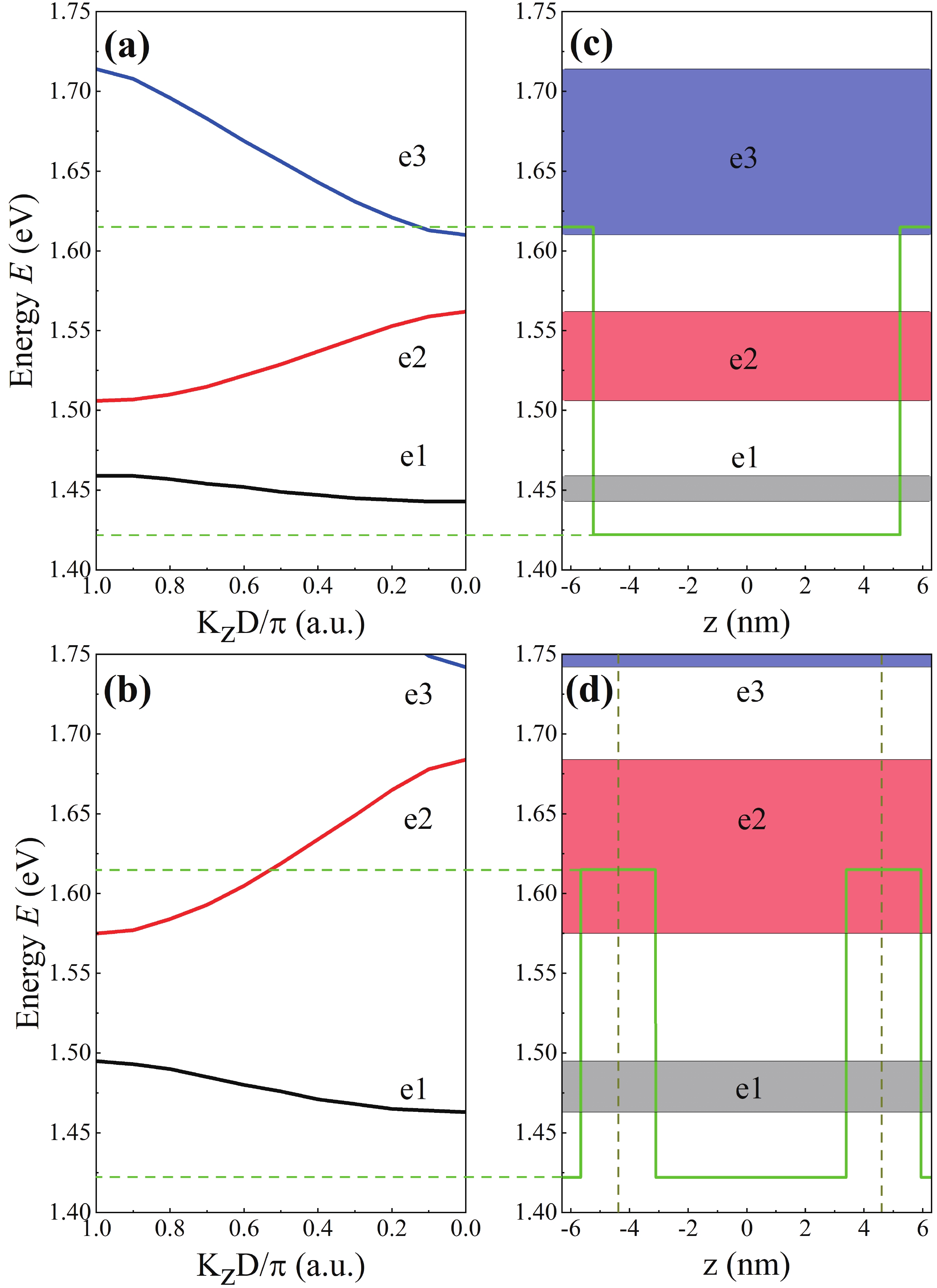
Fig. 2.  (Color online) The electronic energy-band structure calculated by Kane model corresponding to sample no. 1 and 2 from Table 1. (a) Electronic energy-band structure of the SMP SL no. 1. (b) Electronic energy-band structure of the SMP SL no. 2. (c) Electronic subband energies and bandwidth of the SMP SL no. 1. (d) Electronic subband energies and bandwidth of the SMP SL no. 2.

The above-mentioned results can be also illustrated as the electronic minibands in the conduction band in Fig. 2. Figs. 2(a) and 2(b) show the relevant E(K) dependences for the electronic states, where K varies within the Brillouin zone of the SL ((Kz0,Kx,Ky=0)). The sizes along the z-dimension of the unit cell of the SLs in the model are D = 12.4 and D = 9.05 nm, respectively. From these figures, one can conclude that the third electronic subband e3 for SL no. 1 is partially localized within the well. As a result, its PR spectrum has optical transitions involving e3 not only at point Г but also at point П (edge of Brillouin zone of the SL) with above-barrier energy levels (see Fig. 2(с)).

Within the scope of the considered, it was assumed that the profile of quantum wells in the superlattice is rectangular (trapezoidal—under electric fields) with abrupt interfaces. The distortions of the conduction/valence bands profiles were neglected due to the insignificant magnitude for the considered doping concentrations. The presence of sharp interfaces was shown by the results of HR HAADF STEM, HRXRR, DXRR, HRXRD investigations. To compensate the minor distortions of the potential profile, the size of a single SL period for the first sample (with period 12 nm) was increased by one GaAs monolayer to obtain better convergence.

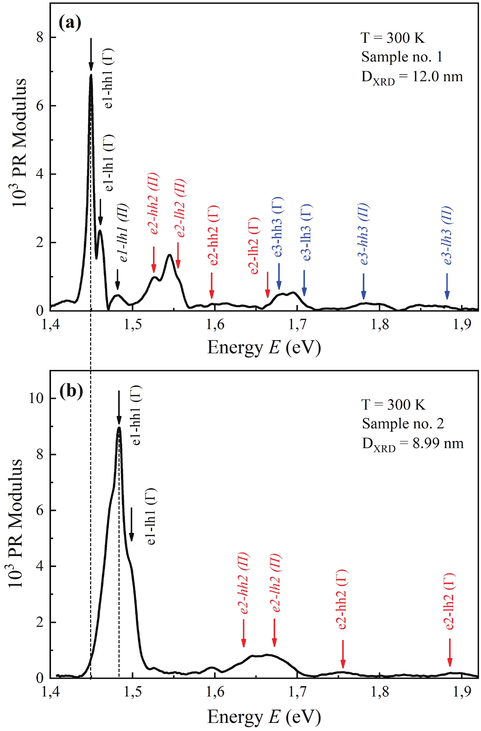
Electronic energy spectra calculated by the Kane model (Table 3, Fig. 2) were consistent with transformed PR spectra of the synthesized Al0.3Ga0.7As/GaAs SMP SLs (Fig. 3). The comparison between experimental and theoretical data allowed us to interpret transformed PR spectra in detail. All the simulated transitions are presented on obtained spectra in Fig. 3 with colored solid arrows. The small broadening of spectral lines shown in Fig. 3(a) confirms the high quality of SMP SL samples. The most intensive and narrow spectral line at 1.449 eV corresponds to the main optical interband transition e1−hh1 at the Г point (center of the Brillouin zone of the SL). The next less intensive peak at 1.461 eV corresponds to the e1−lh1 transition at the Г point. The high quality of the SL has led to a small broadening of spectral lines and these two peaks with extrema position difference of 12 meV turned out to be resolved even at room temperature. Their position, as well as the position of other marked peaks, is in good agreement with the Kane model calculations.

Fig. 3.  (Color online) Transformed PR spectra of samples no.1 (a) and no. 2 (b) from Table 1 measured at T = 300 K.

Fig. 3 also compares the transformed PR spectra of the superlattices samples no. 1 (Fig. 3(a)) and no. 2 (Fig. 3(b)) with periods D = 12.0 nm and 8.99 nm, respectively. A decrease in the superlattice period from 12.0 to 9 nm led to a significant increase in the same optical transition energies observed in the spectrum (Fig. 3(b)). The main optical transition in sample no. 2 increased in energy up to 1.483 eV. The left shoulder of the main optical transition peak in the transformed spectrum is assumed to be associated with the impurity exciton state. According to Kane model calculations with such SL configuration, two electron subbands are formed, while the second subband is only partially localized within the well (see Fig. 2(с)). As a result, relatively intense transitions are observed in the spectrum with the participation of the e2 subband at the П point around 1.63−1.68 eV and less intense transitions at the Г point with above-barrier transitions.

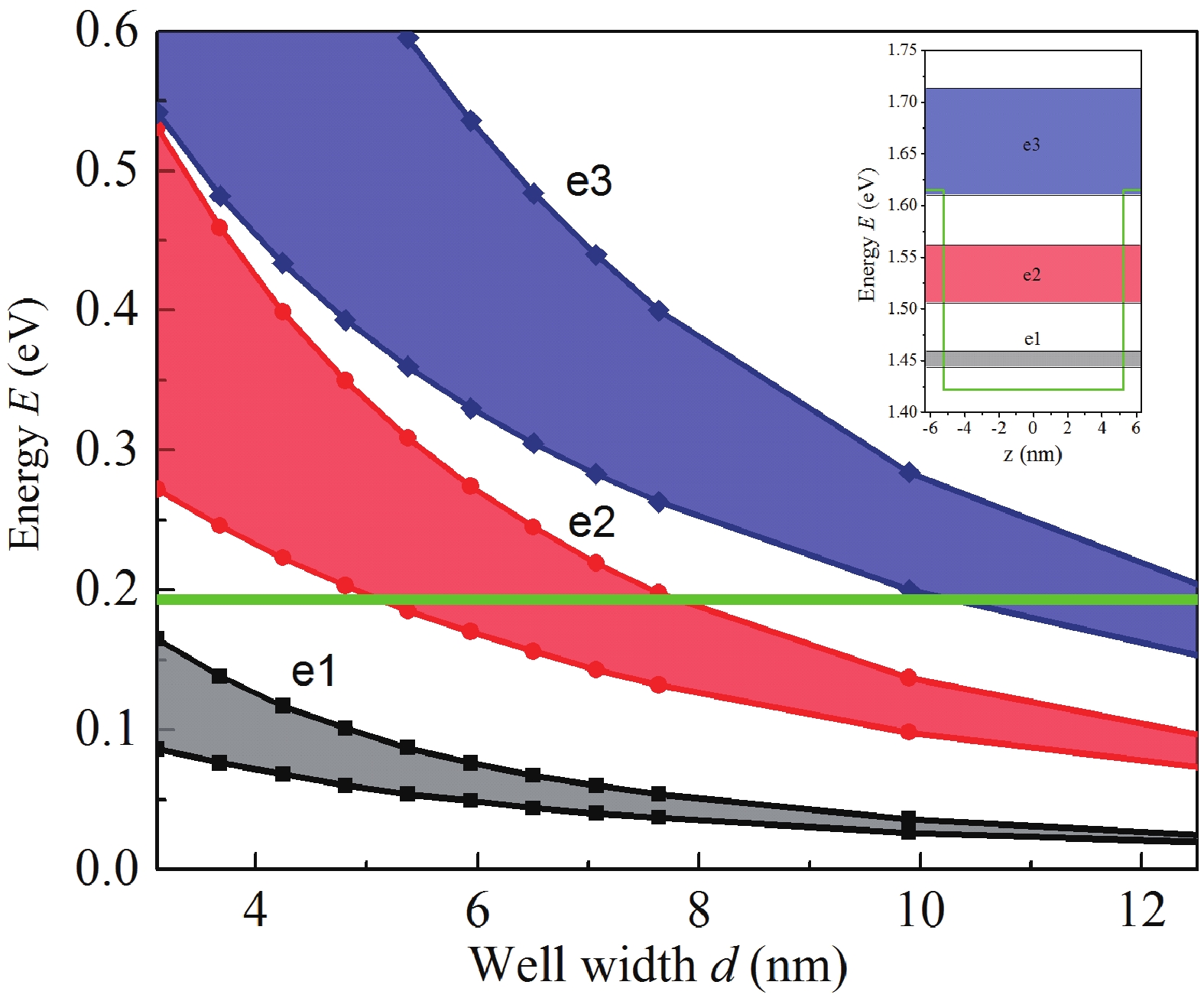
The difference between experimentally obtained and computed transition energies does not exceed several meV. The proposed Kane model allowed us to significantly reduce the error of the peak positions from 25% to 1%−5%. Also, using the Kane model, it became possible to obtain the precise position of minibands in the range of SL designs (Fig. 4). Obtained results show smooth dependence from the width of the well. It is also worth mentioning that there is a threshold width value of 5 nm. For more narrow quantum wells, the expectation is that the second eigenstate won’t be observable in PR analysis.

Fig. 4.  (Color online) Electronic subband energies and bandwidth calculated by the Kane model as a function of well thickness, with a fixed barrier thickness of 2 nm. The energy zero coincides with the GaAs conduction band edge. The graph exhibits the positions for both Γ and Π point in the Brillouin zone of the SLs. The solid light green horizontal line represents the position of the Al0.3Ga0.7As (barrier layers) conduction band edge. The inset contains the energy-band diagram demonstrated in Fig. 2(c).

The Kane model described above is highly accurate, but it can simulate the band diagram and electronic energy spectrum only. This model is not intended to calculate electronic transition rates between corresponding energy states. Therefore, other methods, that consider electronic transitions, should be used to estimate scattering rates and gain. Since CSM, described earlier, can calculate these characteristics, we decided to combine the 8-band kp-model with the “shooting approach”. The simulation process of our method can be divided into the following steps:

(1) initially, energy level positions (their vicinity), effective masses, theoretical period of SL, etc. were computed with the Kane model;

(2) computed parameters were fed to CSM to obtain the accurate solution of the Schrödinger equation, i.e., the eigenvalues and eigenvectors for the given Hamiltonian;

(3) the figures of merit, transition rates, and gain estimates were calculated by MC approach and Eqs. (1)−(4) with eigenvalues and eigenvectors, obtained in the previous step.

This sequence of steps preserves the accuracy of the Kane model and allows to estimate gain. Thus, this method has all the prerequisites to become a new and more reliable alternative to commonly used approaches.

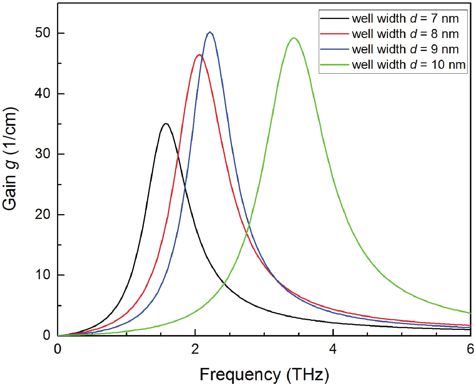
To get the highest gain estimate and maintain the frequency of amplified light in the THz range, we have varied the thickness of the quantum well between 7 and 10 nm. The results obtained by our new method are presented in Fig. 5Fig. 7. All of the below-mentioned computations were performed for the temperature of 300 K. Fig. 5 demonstrates the frequency dependence of the estimated gain for different quantum well thicknesses. The graph illustrates that wider quantum wells provide higher gain values, but the radiation frequency is blue-shifted towards 2.5 THz. Presumably, the higher gain values are achieved due to the increased wave function localization in wider wells.

Fig. 5.  (Color online) Simulated gain vs. radiation frequency for SMP SL with quantum well thicknesses between 7 and 10 nm and a fixed barrier thickness of 2 nm.

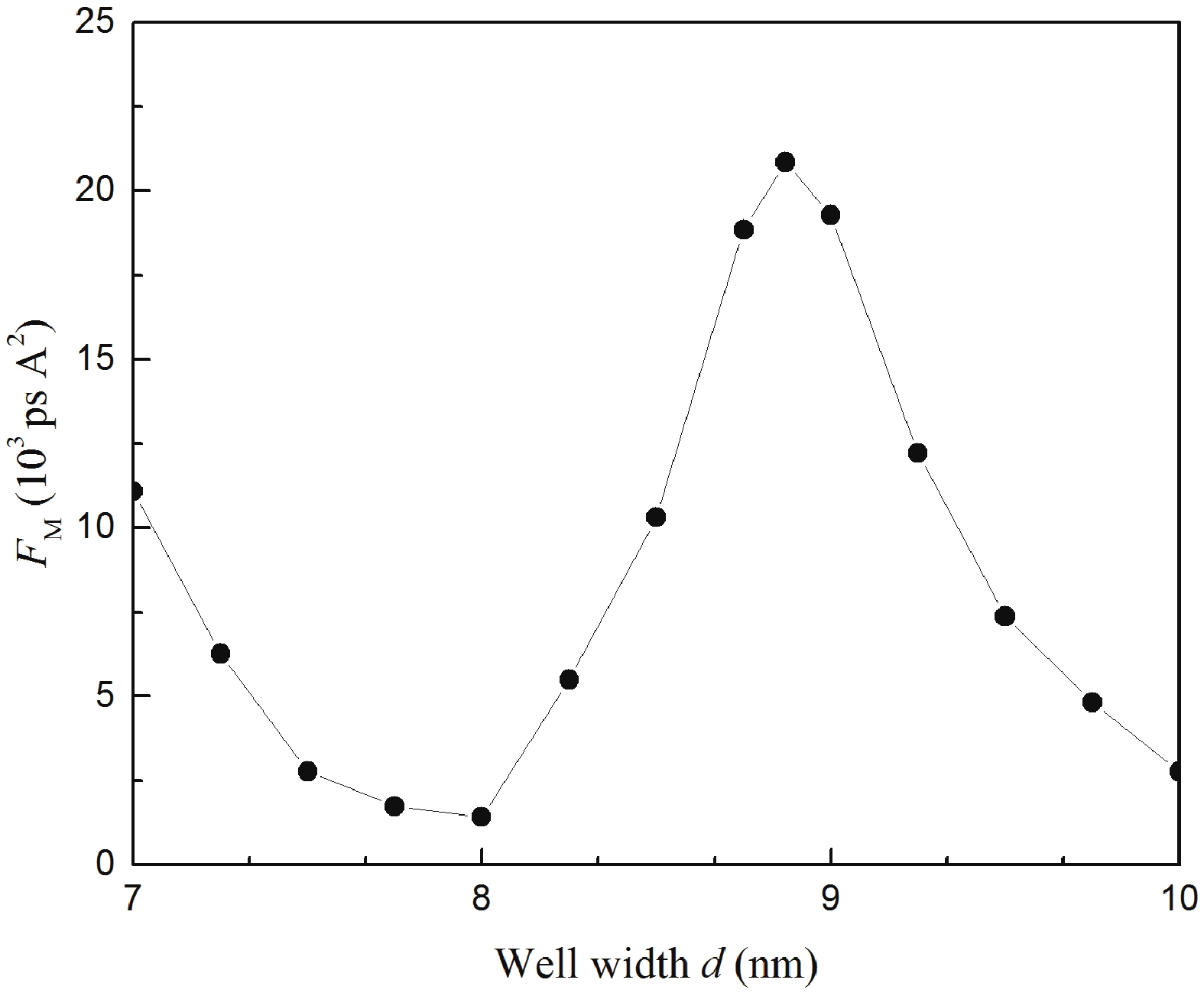
Fig. 6 shows the figure of merit dependence on the quantum well thickness. The plot confirms that wider quantum wells result in higher gain, as shown by the figure of merit dependence on quantum well width. According to this graph, the most suitable width values, where the highest FM can be obtained, are between 8.5 and 9.5 nm. The maximum position is expected to be at 8.8 nm.

Fig. 6.  The computed figure of merit values vs. quantum well width for SLs with a fixed barrier thickness of 2 nm.
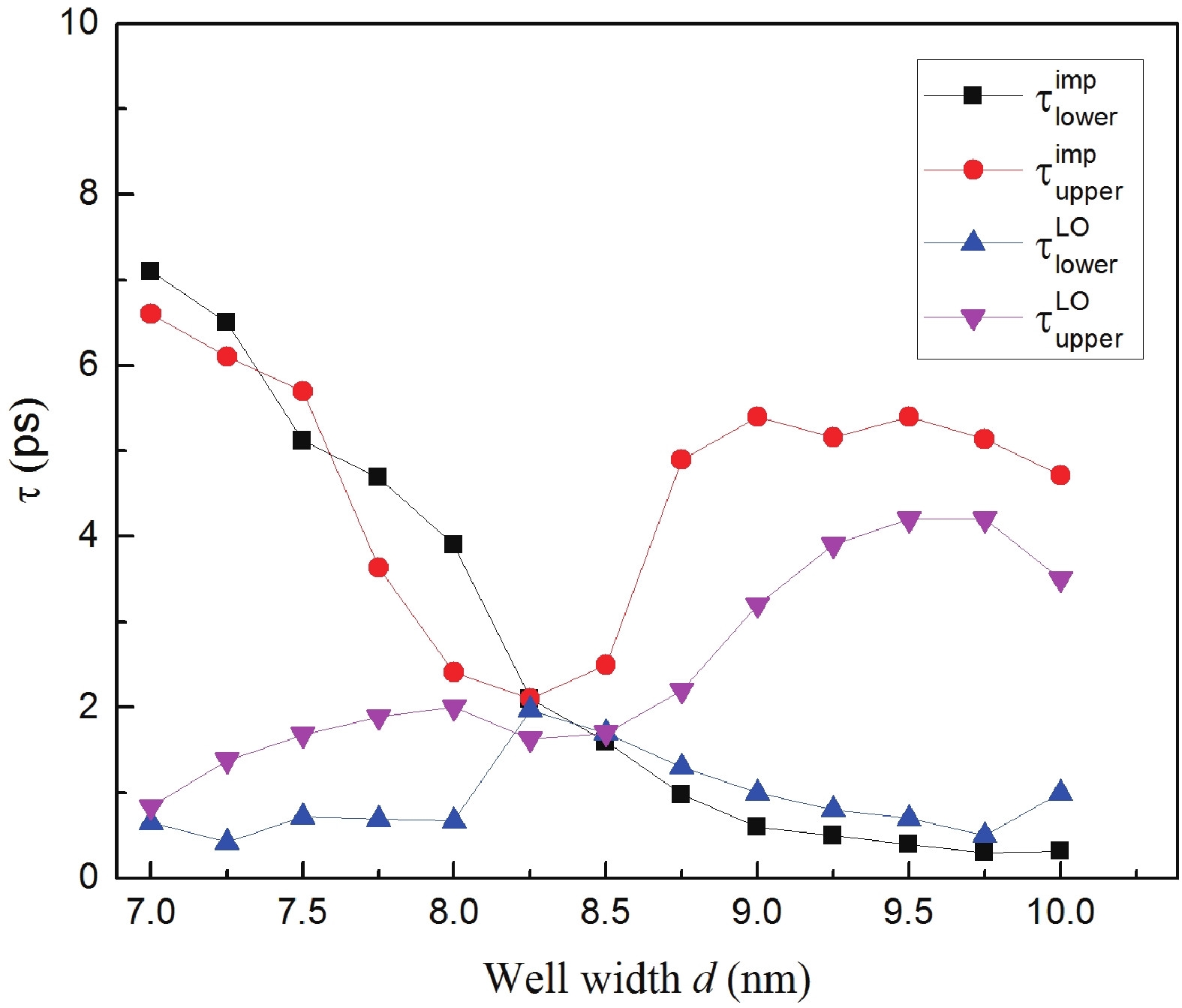
Fig. 7.  (Color online) Simulated scattering times of upper and lower level for two mechanisms: LO-phonon (LO), impurity scattering (imp) vs. quantum well width for SLs with a fixed barrier thickness of 2 nm.

Scattering rates for LO-phonon and impurity mechanisms were also calculated during simulations, and their dependency on quantum well width is shown in Fig. 7. Shorter scattering times result in faster depopulation of the level, i.e., designs with longer scattering times for the upper level and shorter times for the lower level are the most convenient for the population inversion maintenance. Therefore, the most suitable region in Fig. 7 is between 8.5 and 10 nm:

• scattering times for the lower level at their minima (they do not exceed 1.5 ps);

• scattering times for the upper level are relatively high (approximately 5 ps).

To summarize all the mentioned results, the most promising structure for a THz source implementation is a considered SMP SL with an 8.5 nm thick quantum well. This geometry provides a higher gain estimate and allows to maintain population inversion with small broadening values γ.

The described combination of PR and Kane model can be used in a more self-contained manner. To show that, the authors also enhanced this method with the process of naïve optimization, where all the following ranges of SL parameters are brute-forced: mole fraction of Al in barrier layers between 10% and 40%, well thickness from 4 to 15 nm. Achieved minimum deviation met expectations, and its position was in good agreement with XRD data and growth parameters. By changing the thickness of the well, one can also control the number of eigenstates inside the SL. As was previously shown, wider quantum wells contain a third undesirable energy level[9]. The proposed method predicted the escape of the second energy level when reducing quantum well thickness, which is illustrated in Fig. 2.

To minimize the adverse impact of elastic scattering, it is suggested to increase the number of periods and decrease the doping concentration of the layers. According to the estimations (Fig. 5), this must significantly decrease (down to several magnitudes) the influence of the elastic scattering, while maintaining high gain values. With the above-described adjusted energy values from the Kane model, the dipole matrix element, relaxation times, and the estimation of the gain coefficient were calculated (Fig. 5Fig. 7). Obtained values showed a gain slightly above 40 cm−1 for the proposed SL with a quantum well layer thickness of 8 nm. We assume that the gain values (see Fig. 5) are significant enough to produce light emission, as the total expected losses are estimated to be below 15 cm−1. To estimate the waveguide loss, we considered the double metal waveguide from Ref. [55]. It should be also mentioned that this structure is the best for light amplification due to the electron transport estimations that exhibit a positive differential conductivity region near the operating point[9, 11].

In conclusion, this paper presents the first and unique comprehensive theoretical analysis of the energy band diagram for super-multiperiod superlattices, verified by experimental data. The authors have developed a new combined method for the theoretical study of multiperiod superlattices. It fuses the precision of the Kane model and the flexibility of the shooting method with the Monte Carlo technique, which results in a more refined and versatile approach. This method was applied to analyze state-of-the-art samples of super-multiperiod superlattices grown by molecular beam epitaxy. The express room-temperature method of photoreflectance was used for experimental approbation. The proposed method diminished the error in the identification of the transition energy peaks to just 5%, presenting a substantial improvement compared to the typical 25% error obtained with conventional approaches. The photoreflectance experiments validated the accuracy and reliability of the combined method. The approach successfully predicted the escape of the second energy level in structures with quantum well thicknesses below 5 nm. The authors reinforced the method with naïve optimization to restore the intrinsic superlattice parameters. The recovered parameters correlated well with X-ray diffractometric data and growth parameters.

The refined method is also suitable for calculating transition rates and estimating gain. Therefore, it was used to design a new light-amplifying super-multiperiod superlattice. Additionally, the authors revealed ways to reduce the impact of elastic scattering in these constructions. The scheme developed in the research boosts the creation of both efficient light amplification and adjustable sources of terahertz and infrared radiation.

Supplementary materials to this article can be found online at https://doi.org/10.1088/1674-4926/45/2/022701.https://doi.org/10.1088/1674-4926/45/2/022701.

The work was supported by the Ministry of Education and Science of the Russian Federation in the framework of experimental research (Nos. 075-01438-22-06 and FSEE-2022-0018) and the Russian Science Foundation in theoretical research (No. RSF 23-29-00216).


[1]
Herman M A. Semiconductor superlattices. Berlin: Akademie-Verlag, 1986
[2]
Xing F, Ji G, Li Z, et al. Preparation, properties and applications of two-dimensional superlattices. Mater Horiz, 2023, 10(3), 722 doi: 10.1039/D2MH01206E
[3]
Jansen M, Tisdale W A, Wood V. Nanocrystal phononics. Nat Mater, 2023, 22(2), 161 doi: 10.1038/s41563-022-01438-4
[4]
Khalatpour A, Paulsen A K, Deimert C, et al. High-power portable terahertz laser systems. Nat Photonics, 2021, 15(1), 16 doi: 10.1038/s41566-020-00707-5
[5]
Gmachl C, Capasso F, Sivco D L, et al. Recent progress in quantum cascade lasers and applications. Rep Prog Phys, 2001, 64(11), 1533 doi: 10.1088/0034-4885/64/11/204
[6]
Mattsson M O, Simkó M. Emerging medical applications based on non-ionizing electromagnetic fields from 0 Hz to 10 THz. Med Devices: Evid Res, 2019, 12, 347 doi: 10.2147/MDER.S214152
[7]
Baxter J B, Guglietta G W. Terahertz spectroscopy. Anal Chem, 2011, 83(12), 4342 doi: 10.1021/ac200907z
[8]
Andronov A A, Ikonnikov A V, Maremianin K V, et al. THz stimulated emission from simple superlattice in positive differential conductivity region. Semicond, 2018, 52, 431 doi: 10.1134/S1063782618040048
[9]
Gerchikov L G, Dashkov A S, Goray L I, et al. Development of the design of super-multiperiod structures grown by molecular-beam epitaxy and emitting in the terahertz range. J Exp Theor Phys, 2021, 133, 161 doi: 10.1134/S1063776121070037
[10]
Belkin M A, Capasso F. New frontiers in quantum cascade lasers: high performance room temperature terahertz sources. Phys Scr, 2015, 90(11), 118002 doi: 10.1088/0031-8949/90/11/118002
[11]
Winge D O, Franckié M, Wacker A. Superlattice gain in positive differential conductivity region. AIP Adv, 2016, 6(4), 045025 doi: 10.1063/1.4948538
[12]
Goray L I, Pirogov E V, Svechnikov M V, et al. High-precision characterization of super-multiperiod AlGaAs/GaAs superlattices using X-ray reflectometry on a synchrotron source. Tech Phys Lett, 2021, 47(10), 757 doi: 10.1134/S1063785021080071
[13]
Goray L I, Pirogov E V, Sobolev M S, et al. Matched characterization of super-multiperiod superlattices. J Phys D, 2020, 53(45), 455103 doi: 10.1088/1361-6463/aba4d6
[14]
Dashkov A S, Gerchikov L G, Goray L I, et al. Sources of terahertz radiation on AlGaAs/GaAs superlattices. Bull Russ Acad Sci Phys, 2023, 87(6), 795 doi: 10.3103/S1062873823702179
[15]
Goray L I, Pirogov E V, Sobolev M S, et al. Matched X-ray reflectometry and diffractometry of super-multiperiod heterostructures grown by molecular beam epitaxy. Semicond, 2019, 53, 1910 doi: 10.1134/S1063782619140082
[16]
Goray L I, Pirogov E V, Sobolev M S, et al. Deep X-ray reflectometry of supermultiperiod A3B5 structures with quantum wells grown by molecular-beam epitaxy. Tech Phys, 2020, 65, 1822 doi: 10.1134/S1063784220110134
[17]
Wacker A. Semiconductor superlattices: a model system for nonlinear transport. Phys Rep, 2002, 357(1), 1 doi: 10.1016/S0370-1573(01)00029-1
[18]
Goray L I, Pirogov E V, Nikitina E V, et al. Photoluminescence and transmission electron microscopy methods for characterization of super-multiperiod A3B5 quantum well structures. Semicond, 2019, 53, 1914 doi: 10.1134/S1063782619140094
[19]
Misiewicz J, Sitarek P, Sek G, et al. Semiconductor heterostructures and device structures investigated by photoreflectance spectroscopy. Mater Sci, 2003, 21(3), 263
[20]
Komkov O S. Infrared photoreflectance of III–V semiconductor materials. Phys Solid State, 2021, 63, 1181 doi: 10.1134/S1063783421080126
[21]
Rogowicz E, Kopaczek J, Polak M P, et al. Carrier dynamics in (Ga, In)(Sb, Bi)/GaSb quantum wells for laser applications in the mid-infrared spectral range. Sci Rep, 2022, 12(1), 12961 doi: 10.1038/s41598-022-16966-x
[22]
Cretì A, Prete P, Lovergine N, et al. Enhanced optical absorption of GaAs near-band-edge transitions in GaAs/AlGaAs core–shell nanowires: implications for nanowire solar cells. ACS Appl Nano Mater, 2022, 5(12), 18149 doi: 10.1021/acsanm.2c04044
[23]
Goryacheva V D, Mironova M S, Komkov O S. Investigation of GaAs/AlGaAs superlattice by photoreflectance method. J Phys: Conf Ser, 2018, 1038(1), 012124 doi: 10.1088/1742-6596/1038/1/012124
[24]
Kudrawiec R, Se̢k G, Ryczko K, et al. Photoreflectance investigations of oscillator strength and broadening of optical transitions for GaAsSb–GaInAs/GaAs bilayer quantum wells. Appl Phys Lett, 2004, 84(18), 3453 doi: 10.1063/1.1737065
[25]
Pikhtin A N, Komkov O S, Bugge F. Effect of electric field on the probability of optical transitions in InGaAs/GaAs quantum wells observed by photo- and electroreflectance methods. Phys Status Solidi, 2005, 202(7), 1270 doi: 10.1002/pssa.200460912
[26]
Rygała M, Ryczko K, Smołka T, et al. Investigating the physics of higher-order optical transitions in InAs/GaSb superlattices. Phys Rev B, 2021, 104(8), 085410 doi: 10.1103/PhysRevB.104.085410
[27]
Shanabrook B V, Glembocki O J, Beard W T. Photoreflectance modulation mechanisms in GaAs-AlxGa1-xAs multiple quantum wells. Phys Rev B, 1987, 35(5), 2540 doi: 10.1103/PhysRevB.35.2540
[28]
Ferizović D, Peng L, Sultana H, et al. Photoreflectance spectroscopy study of a strained-layer CdTe/ZnTe superlattice. J Appl Phys, 2011, 110(9), 093703 doi: 10.1063/1.3657785
[29]
Motyka M, Janiak F, Misiewicz J, et al. Determination of energy difference and width of minibands in GaAs/AlGaAs superlattices by using Fourier transform photoreflectance and photoluminescence. Opto−Electron Rev, 2011, 19(2), 151 doi: 10.2478/s11772-011-0021-7
[30]
Janiak F, Dyksik M, Motyka M, et al. Advanced optical characterization of AlGaAs/GaAs superlattices for active regions in quantum cascade lasers. Opt Quantum Electron, 2015, 47, 945 doi: 10.1007/s11082-014-9991-2
[31]
Hosea T J C. Estimating critical-point parameters of modulated reflectance spectra. Phys Status Solidi B, 1995, 189(2), 531 doi: 10.1002/pssb.2221890221
[32]
Jirauschek C, Kubis T. Modeling techniques for quantum cascade lasers. Appl Phys Rev, 2014, 1(1), 011307 doi: 10.1063/1.4863665
[33]
Vukmirović N, Wang L W. Quantum dots: theory. In comprehensive nanoscience and technology. London: Academic Press, 2011
[34]
Glinskii G F, Lakisov V A, Dolmatov A G, et al. Multiband coupling and electronic structure of short-period (GaAs)n/(AlAs)n (001) superlattices. Nanotechnology, 2000, 11(4), 233 doi: 10.1088/0957-4484/11/4/308
[35]
Glinskii G F, Mironova M S. Effective Hamiltonians for heterostructures based on direct-gap III–V semiconductors. The kp perturbation theory and the method of invariants. Semicond, 2014, 48, 1324 doi: 10.1134/S106378261410008X
[36]
Mironova M S, Komkov O S, Firsov D D, et al. Determination of InSb/AlInSb quantum well energy spectrum. J Phys: Conf Ser, 2014, 541(1), 012085 doi: 10.1088/1742-6596/541/1/012085
[37]
Dashkov A S, Kostromin N A, Babichev A V, et al. Simulation of the energy-band structure of superlattice of quaternary alloys of diluted nitrides. Semicond, 2023, 57(3), 207 doi: 10.21883/SC.2023.03.56237.4163
[38]
Liu P Q, Hoffman A J, Escarra M D, et al. Highly power-efficient quantum cascade lasers. Nat Photonics, 2010, 4(2), 95 doi: 10.1038/nphoton.2009.262
[39]
Callebaut H, Hu Q. Importance of coherence for electron transport in terahertz quantum cascade lasers. J Appl Phys, 2005, 98(10), 104505 doi: 10.1063/1.2136420
[40]
Matyas A, Lugli P, Jirauschek C. Role of collisional broadening in Monte Carlo simulations of terahertz quantum cascade lasers. Appl Phys Lett, 2013, 102(1), 011101 doi: 10.1063/1.4773516
[41]
Ando T, Fowler A B, Stern F. Electronic properties of two-dimensional systems. Rev Mod Phys, 1982, 54(2), 437 doi: 10.1103/RevModPhys.54.437
[42]
Pereira Jr M F, Lee S C, Wacker A. Controlling many-body effects in the midinfrared gain and terahertz absorption of quantum cascade laser structures. Phys Rev B, 2004, 69(20), 205310 doi: 10.1103/PhysRevB.69.205310
[43]
Tamosiunas V, Zobl R, Ulrich J, et al. Terahertz quantum cascade lasers in a magnetic field. Appl Phys Lett, 2003, 83(19), 3873 doi: 10.1063/1.1626018
[44]
Huang W, Rassel S S, Li L, et al. A unified figure of merit for interband and intersubband cascade devices. Infrared Phys Technol, 2019, 96, 298 doi: 10.1016/j.infrared.2018.11.033
[45]
Laturia A A, Van de Put M L, Vandenberghe W G. Generation of empirical pseudopotentials for transport applications and their application to group IV materials. J Appl Phys, 2020, 128(3), 034306 doi: 10.1063/5.0009838
[46]
Lee B G, Luo J W, Neale N R, et al. Quasi-direct optical transitions in silicon nanocrystals with intensity exceeding the bulk. Nano Lett, 2016, 16(3), 1583 doi: 10.1021/acs.nanolett.5b04256
[47]
Xiong J X, Guan S, Luo J W, et al. Emergence of strong tunable linear Rashba spin-orbit coupling in two-dimensional hole gases in semiconductor quantum wells. Phys Rev B, 2021, 103(8), 085309 doi: 10.1103/PhysRevB.103.085309
[48]
Avdeev I D, Belolipetsky A V, Ha N N, et al. Absorption of Si, Ge, and SiGe alloy nanocrystals embedded in SiO2 matrix. J Appl Phys, 2020, 127(11), 114301 doi: 10.1063/1.5139960
[49]
Glinskii G F, Mironova M S. An 8-band Kane model for quantum-sized heterostructures based on cubic semiconductors A3B5. J Phys: Conf Ser, 2013, 572(1), 012052 doi: 10.1088/1742-6596/572/1/012052
[50]
Glinskii G F, Andrianov A V, Sreseli O M, et al. Terahertz electroluminescence originating from spatially indirect intersubband transitions in a GaAs/AlGaAs quantum-cascade structure. Semicond, 2005, 39, 1182 doi: 10.1134/1.2085267
[51]
Glinskii G F. A simple numerical method for determining the energy spectrum of charge carriers in semiconductor heterostructures. Tech Phys Lett, 2018, 44, 232 doi: 10.1134/S1063785018030161
[52]
Glinskii G F, Shapran D A. The energy spectrum and wave functions of electrons in tunnel-coupled spherical InAs/GaAs quantum dots. Tech Phys Lett, 2020, 46, 272 doi: 10.1134/S1063785020030219
[53]
Firsov D D, Komkov O S, Solov’ev V A, et al. Infrared photoreflectance of InSb-based two-dimensional nanostructures. J Opt Soc Am B, 2019, 36(4), 910 doi: 10.1364/JOSAB.36.000910
[54]
Vurgaftman I, Meyer J R, Ram-Mohan L R. Band parameters for III–V compound semiconductors and their alloys. J Appl Phys, 2001, 89(11), 5815 doi: 10.1063/1.1368156
[55]
Williams B S. Terahertz quantum-cascade lasers. Nat Photonics, 2007, 1(9), 517 doi: 10.1038/nphoton.2007.166
Fig. 1.  (Color online) The transformed PR spectrum of sample no. 1 measured at T = 300 K. Black dotted arrows indicate the experimental transition energy peaks and green solid arrows indicate the transition energy positions computed by CSM.

Fig. 2.  (Color online) The electronic energy-band structure calculated by Kane model corresponding to sample no. 1 and 2 from Table 1. (a) Electronic energy-band structure of the SMP SL no. 1. (b) Electronic energy-band structure of the SMP SL no. 2. (c) Electronic subband energies and bandwidth of the SMP SL no. 1. (d) Electronic subband energies and bandwidth of the SMP SL no. 2.

Fig. 3.  (Color online) Transformed PR spectra of samples no.1 (a) and no. 2 (b) from Table 1 measured at T = 300 K.

Fig. 4.  (Color online) Electronic subband energies and bandwidth calculated by the Kane model as a function of well thickness, with a fixed barrier thickness of 2 nm. The energy zero coincides with the GaAs conduction band edge. The graph exhibits the positions for both Γ and Π point in the Brillouin zone of the SLs. The solid light green horizontal line represents the position of the Al0.3Ga0.7As (barrier layers) conduction band edge. The inset contains the energy-band diagram demonstrated in Fig. 2(c).

Fig. 5.  (Color online) Simulated gain vs. radiation frequency for SMP SL with quantum well thicknesses between 7 and 10 nm and a fixed barrier thickness of 2 nm.

Fig. 6.  The computed figure of merit values vs. quantum well width for SLs with a fixed barrier thickness of 2 nm.

Fig. 7.  (Color online) Simulated scattering times of upper and lower level for two mechanisms: LO-phonon (LO), impurity scattering (imp) vs. quantum well width for SLs with a fixed barrier thickness of 2 nm.

Table 1.   Parameters of the AlxGa1-xAs/GaAs superlattices samples under study.

No. Al(%) Doping level
(сm−3)
Number of periods
(counts)
Well thickness (nm) Barrier thickness (nm) Designed period
(nm)
Period from XRD
(nm)
1 30 1016 100 10 2 12 12.0
2 30 1016 100 7 2 9 8.99
DownLoad: CSV

Table 2.   The band structure parameters used in the Kane model calculations at T = 300 K.

Parameter Material
GaAs AlAs AlxGa1xAs
a (Å) 5.6532 5 5.6611 aAlAsx+aGaAs(1x)
E(Γ)g(eV) 1.422 3.003 EAlAsx+EGaAs(1x)+(0.127+1.310x)(1x)
Δso(eV) 0.341 0.28 ΔAlAsx+ΔGaAs(1x)
me(Γ) 0.067 0.124
γL1 6.98 3.76
γL2 2.06 0.82
γL3 2.93 1.42
EP(eV) 28.8 21.1 EPAlAsx+EPGaAs(1x)
DownLoad: CSV

Table 3.   Values of the optical transition energies (eV) calculated with the Kane model.

Transition type Point in k-space
Sample no. 1 Sample no. 2
Г П Г П
e1−hh1 1.449 1.466 1.486 1.516
e1−lh1 1.454 1.485 1.497 1.549
e2−hh2 1.591 1.529 1.763 1.647
e2−lh2 1.655 1.556 1.876 1.691
e3−hh3 1.662 1.779
e3−lh3 1.729 1.895
DownLoad: CSV
[1]
Herman M A. Semiconductor superlattices. Berlin: Akademie-Verlag, 1986
[2]
Xing F, Ji G, Li Z, et al. Preparation, properties and applications of two-dimensional superlattices. Mater Horiz, 2023, 10(3), 722 doi: 10.1039/D2MH01206E
[3]
Jansen M, Tisdale W A, Wood V. Nanocrystal phononics. Nat Mater, 2023, 22(2), 161 doi: 10.1038/s41563-022-01438-4
[4]
Khalatpour A, Paulsen A K, Deimert C, et al. High-power portable terahertz laser systems. Nat Photonics, 2021, 15(1), 16 doi: 10.1038/s41566-020-00707-5
[5]
Gmachl C, Capasso F, Sivco D L, et al. Recent progress in quantum cascade lasers and applications. Rep Prog Phys, 2001, 64(11), 1533 doi: 10.1088/0034-4885/64/11/204
[6]
Mattsson M O, Simkó M. Emerging medical applications based on non-ionizing electromagnetic fields from 0 Hz to 10 THz. Med Devices: Evid Res, 2019, 12, 347 doi: 10.2147/MDER.S214152
[7]
Baxter J B, Guglietta G W. Terahertz spectroscopy. Anal Chem, 2011, 83(12), 4342 doi: 10.1021/ac200907z
[8]
Andronov A A, Ikonnikov A V, Maremianin K V, et al. THz stimulated emission from simple superlattice in positive differential conductivity region. Semicond, 2018, 52, 431 doi: 10.1134/S1063782618040048
[9]
Gerchikov L G, Dashkov A S, Goray L I, et al. Development of the design of super-multiperiod structures grown by molecular-beam epitaxy and emitting in the terahertz range. J Exp Theor Phys, 2021, 133, 161 doi: 10.1134/S1063776121070037
[10]
Belkin M A, Capasso F. New frontiers in quantum cascade lasers: high performance room temperature terahertz sources. Phys Scr, 2015, 90(11), 118002 doi: 10.1088/0031-8949/90/11/118002
[11]
Winge D O, Franckié M, Wacker A. Superlattice gain in positive differential conductivity region. AIP Adv, 2016, 6(4), 045025 doi: 10.1063/1.4948538
[12]
Goray L I, Pirogov E V, Svechnikov M V, et al. High-precision characterization of super-multiperiod AlGaAs/GaAs superlattices using X-ray reflectometry on a synchrotron source. Tech Phys Lett, 2021, 47(10), 757 doi: 10.1134/S1063785021080071
[13]
Goray L I, Pirogov E V, Sobolev M S, et al. Matched characterization of super-multiperiod superlattices. J Phys D, 2020, 53(45), 455103 doi: 10.1088/1361-6463/aba4d6
[14]
Dashkov A S, Gerchikov L G, Goray L I, et al. Sources of terahertz radiation on AlGaAs/GaAs superlattices. Bull Russ Acad Sci Phys, 2023, 87(6), 795 doi: 10.3103/S1062873823702179
[15]
Goray L I, Pirogov E V, Sobolev M S, et al. Matched X-ray reflectometry and diffractometry of super-multiperiod heterostructures grown by molecular beam epitaxy. Semicond, 2019, 53, 1910 doi: 10.1134/S1063782619140082
[16]
Goray L I, Pirogov E V, Sobolev M S, et al. Deep X-ray reflectometry of supermultiperiod A3B5 structures with quantum wells grown by molecular-beam epitaxy. Tech Phys, 2020, 65, 1822 doi: 10.1134/S1063784220110134
[17]
Wacker A. Semiconductor superlattices: a model system for nonlinear transport. Phys Rep, 2002, 357(1), 1 doi: 10.1016/S0370-1573(01)00029-1
[18]
Goray L I, Pirogov E V, Nikitina E V, et al. Photoluminescence and transmission electron microscopy methods for characterization of super-multiperiod A3B5 quantum well structures. Semicond, 2019, 53, 1914 doi: 10.1134/S1063782619140094
[19]
Misiewicz J, Sitarek P, Sek G, et al. Semiconductor heterostructures and device structures investigated by photoreflectance spectroscopy. Mater Sci, 2003, 21(3), 263
[20]
Komkov O S. Infrared photoreflectance of III–V semiconductor materials. Phys Solid State, 2021, 63, 1181 doi: 10.1134/S1063783421080126
[21]
Rogowicz E, Kopaczek J, Polak M P, et al. Carrier dynamics in (Ga, In)(Sb, Bi)/GaSb quantum wells for laser applications in the mid-infrared spectral range. Sci Rep, 2022, 12(1), 12961 doi: 10.1038/s41598-022-16966-x
[22]
Cretì A, Prete P, Lovergine N, et al. Enhanced optical absorption of GaAs near-band-edge transitions in GaAs/AlGaAs core–shell nanowires: implications for nanowire solar cells. ACS Appl Nano Mater, 2022, 5(12), 18149 doi: 10.1021/acsanm.2c04044
[23]
Goryacheva V D, Mironova M S, Komkov O S. Investigation of GaAs/AlGaAs superlattice by photoreflectance method. J Phys: Conf Ser, 2018, 1038(1), 012124 doi: 10.1088/1742-6596/1038/1/012124
[24]
Kudrawiec R, Se̢k G, Ryczko K, et al. Photoreflectance investigations of oscillator strength and broadening of optical transitions for GaAsSb–GaInAs/GaAs bilayer quantum wells. Appl Phys Lett, 2004, 84(18), 3453 doi: 10.1063/1.1737065
[25]
Pikhtin A N, Komkov O S, Bugge F. Effect of electric field on the probability of optical transitions in InGaAs/GaAs quantum wells observed by photo- and electroreflectance methods. Phys Status Solidi, 2005, 202(7), 1270 doi: 10.1002/pssa.200460912
[26]
Rygała M, Ryczko K, Smołka T, et al. Investigating the physics of higher-order optical transitions in InAs/GaSb superlattices. Phys Rev B, 2021, 104(8), 085410 doi: 10.1103/PhysRevB.104.085410
[27]
Shanabrook B V, Glembocki O J, Beard W T. Photoreflectance modulation mechanisms in GaAs-AlxGa1-xAs multiple quantum wells. Phys Rev B, 1987, 35(5), 2540 doi: 10.1103/PhysRevB.35.2540
[28]
Ferizović D, Peng L, Sultana H, et al. Photoreflectance spectroscopy study of a strained-layer CdTe/ZnTe superlattice. J Appl Phys, 2011, 110(9), 093703 doi: 10.1063/1.3657785
[29]
Motyka M, Janiak F, Misiewicz J, et al. Determination of energy difference and width of minibands in GaAs/AlGaAs superlattices by using Fourier transform photoreflectance and photoluminescence. Opto−Electron Rev, 2011, 19(2), 151 doi: 10.2478/s11772-011-0021-7
[30]
Janiak F, Dyksik M, Motyka M, et al. Advanced optical characterization of AlGaAs/GaAs superlattices for active regions in quantum cascade lasers. Opt Quantum Electron, 2015, 47, 945 doi: 10.1007/s11082-014-9991-2
[31]
Hosea T J C. Estimating critical-point parameters of modulated reflectance spectra. Phys Status Solidi B, 1995, 189(2), 531 doi: 10.1002/pssb.2221890221
[32]
Jirauschek C, Kubis T. Modeling techniques for quantum cascade lasers. Appl Phys Rev, 2014, 1(1), 011307 doi: 10.1063/1.4863665
[33]
Vukmirović N, Wang L W. Quantum dots: theory. In comprehensive nanoscience and technology. London: Academic Press, 2011
[34]
Glinskii G F, Lakisov V A, Dolmatov A G, et al. Multiband coupling and electronic structure of short-period (GaAs)n/(AlAs)n (001) superlattices. Nanotechnology, 2000, 11(4), 233 doi: 10.1088/0957-4484/11/4/308
[35]
Glinskii G F, Mironova M S. Effective Hamiltonians for heterostructures based on direct-gap III–V semiconductors. The kp perturbation theory and the method of invariants. Semicond, 2014, 48, 1324 doi: 10.1134/S106378261410008X
[36]
Mironova M S, Komkov O S, Firsov D D, et al. Determination of InSb/AlInSb quantum well energy spectrum. J Phys: Conf Ser, 2014, 541(1), 012085 doi: 10.1088/1742-6596/541/1/012085
[37]
Dashkov A S, Kostromin N A, Babichev A V, et al. Simulation of the energy-band structure of superlattice of quaternary alloys of diluted nitrides. Semicond, 2023, 57(3), 207 doi: 10.21883/SC.2023.03.56237.4163
[38]
Liu P Q, Hoffman A J, Escarra M D, et al. Highly power-efficient quantum cascade lasers. Nat Photonics, 2010, 4(2), 95 doi: 10.1038/nphoton.2009.262
[39]
Callebaut H, Hu Q. Importance of coherence for electron transport in terahertz quantum cascade lasers. J Appl Phys, 2005, 98(10), 104505 doi: 10.1063/1.2136420
[40]
Matyas A, Lugli P, Jirauschek C. Role of collisional broadening in Monte Carlo simulations of terahertz quantum cascade lasers. Appl Phys Lett, 2013, 102(1), 011101 doi: 10.1063/1.4773516
[41]
Ando T, Fowler A B, Stern F. Electronic properties of two-dimensional systems. Rev Mod Phys, 1982, 54(2), 437 doi: 10.1103/RevModPhys.54.437
[42]
Pereira Jr M F, Lee S C, Wacker A. Controlling many-body effects in the midinfrared gain and terahertz absorption of quantum cascade laser structures. Phys Rev B, 2004, 69(20), 205310 doi: 10.1103/PhysRevB.69.205310
[43]
Tamosiunas V, Zobl R, Ulrich J, et al. Terahertz quantum cascade lasers in a magnetic field. Appl Phys Lett, 2003, 83(19), 3873 doi: 10.1063/1.1626018
[44]
Huang W, Rassel S S, Li L, et al. A unified figure of merit for interband and intersubband cascade devices. Infrared Phys Technol, 2019, 96, 298 doi: 10.1016/j.infrared.2018.11.033
[45]
Laturia A A, Van de Put M L, Vandenberghe W G. Generation of empirical pseudopotentials for transport applications and their application to group IV materials. J Appl Phys, 2020, 128(3), 034306 doi: 10.1063/5.0009838
[46]
Lee B G, Luo J W, Neale N R, et al. Quasi-direct optical transitions in silicon nanocrystals with intensity exceeding the bulk. Nano Lett, 2016, 16(3), 1583 doi: 10.1021/acs.nanolett.5b04256
[47]
Xiong J X, Guan S, Luo J W, et al. Emergence of strong tunable linear Rashba spin-orbit coupling in two-dimensional hole gases in semiconductor quantum wells. Phys Rev B, 2021, 103(8), 085309 doi: 10.1103/PhysRevB.103.085309
[48]
Avdeev I D, Belolipetsky A V, Ha N N, et al. Absorption of Si, Ge, and SiGe alloy nanocrystals embedded in SiO2 matrix. J Appl Phys, 2020, 127(11), 114301 doi: 10.1063/1.5139960
[49]
Glinskii G F, Mironova M S. An 8-band Kane model for quantum-sized heterostructures based on cubic semiconductors A3B5. J Phys: Conf Ser, 2013, 572(1), 012052 doi: 10.1088/1742-6596/572/1/012052
[50]
Glinskii G F, Andrianov A V, Sreseli O M, et al. Terahertz electroluminescence originating from spatially indirect intersubband transitions in a GaAs/AlGaAs quantum-cascade structure. Semicond, 2005, 39, 1182 doi: 10.1134/1.2085267
[51]
Glinskii G F. A simple numerical method for determining the energy spectrum of charge carriers in semiconductor heterostructures. Tech Phys Lett, 2018, 44, 232 doi: 10.1134/S1063785018030161
[52]
Glinskii G F, Shapran D A. The energy spectrum and wave functions of electrons in tunnel-coupled spherical InAs/GaAs quantum dots. Tech Phys Lett, 2020, 46, 272 doi: 10.1134/S1063785020030219
[53]
Firsov D D, Komkov O S, Solov’ev V A, et al. Infrared photoreflectance of InSb-based two-dimensional nanostructures. J Opt Soc Am B, 2019, 36(4), 910 doi: 10.1364/JOSAB.36.000910
[54]
Vurgaftman I, Meyer J R, Ram-Mohan L R. Band parameters for III–V compound semiconductors and their alloys. J Appl Phys, 2001, 89(11), 5815 doi: 10.1063/1.1368156
[55]
Williams B S. Terahertz quantum-cascade lasers. Nat Photonics, 2007, 1(9), 517 doi: 10.1038/nphoton.2007.166
1

Simulation and application of external quantum efficiency of solar cells based on spectroscopy

Guanlin Chen, Can Han, Lingling Yan, Yuelong Li, Ying Zhao, et al.

Journal of Semiconductors, 2019, 40(12): 122701. doi: 10.1088/1674-4926/40/12/122701

2

245 GHz subharmonic receiver with on-chip antenna for gas spectroscopy application

Yanfei Mao, Shiju E, Klaus Schmalz, J. Christoph Scheytt

Journal of Semiconductors, 2018, 39(12): 125001. doi: 10.1088/1674-4926/39/12/125001

3

Schottky barrier parameters and structural properties of rapidly annealed Zr Schottky electrode on p-type GaN

V. Rajagopal Reddy, B. Asha, Chel-Jong Choi

Journal of Semiconductors, 2017, 38(6): 064001. doi: 10.1088/1674-4926/38/6/064001

4

The electronic and magnetic properties of wurtzite Mn:CdS, Cr:CdS and Mn:Cr:CdS: first principles calculations

Azeem Nabi, Zarmeena Akhtar, Tahir Iqbal, Atif Ali, Arshad Javid, et al.

Journal of Semiconductors, 2017, 38(7): 073001. doi: 10.1088/1674-4926/38/7/073001

5

Semiconductor steady state defect effective Fermi level and deep level transient spectroscopy depth profiling

Ken K. Chin, Zimeng Cheng

Journal of Semiconductors, 2016, 37(9): 092003. doi: 10.1088/1674-4926/37/9/092003

6

Modeling the drain current and its equation parameters for lightly doped symmetrical double-gate MOSFETs

Mini Bhartia, Arun Kumar Chatterjee

Journal of Semiconductors, 2015, 36(4): 044003. doi: 10.1088/1674-4926/36/4/044003

7

The storage lifetime model based on multi-performance degradation parameters

Haochun Qi, Xiaoling Zhang, Xuesong Xie, Changzhi Lü

Journal of Semiconductors, 2014, 35(10): 104012. doi: 10.1088/1674-4926/35/10/104012

8

Effect of band gap energy on the electrical conductivity in doped ZnO thin film

Said Benramache, Okba Belahssen, Hachemi Ben Temam

Journal of Semiconductors, 2014, 35(7): 073001. doi: 10.1088/1674-4926/35/7/073001

9

Giant magnetoresistance in a two-dimensional electron gas modulated by ferromagnetic and Schottky metal stripes

Lu Jianduo, Xu Bin

Journal of Semiconductors, 2012, 33(7): 074007. doi: 10.1088/1674-4926/33/7/074007

10

Effect of collector bias current on the linearity of common-emitter BJT amplifiers

Li Kun, Teng Jianfu, Xuan Xiuwei

Journal of Semiconductors, 2010, 31(12): 124012. doi: 10.1088/1674-4926/31/12/124012

11

Photoconductive properties of lead iodide films prepared by electron beam evaporation

Zhu Xinghua, Yang Dingyu, Wei Zhaorong, Sun Hui, Wang Zhiguo, et al.

Journal of Semiconductors, 2010, 31(8): 083002. doi: 10.1088/1674-4926/31/8/083002

12

A novel fully differential telescopic operational transconductance amplifier

Li Tianwang, Ye Bo, Jiang Jinguang

Journal of Semiconductors, 2009, 30(8): 085002. doi: 10.1088/1674-4926/30/8/085002

13

A novel low-voltage operational amplifier for low-power pipelined ADCs

Fan Mingjun, Ren Junyan, Guo Yao, Li Ning, Ye Fan, et al.

Journal of Semiconductors, 2009, 30(1): 015009. doi: 10.1088/1674-4926/30/1/015009

14

1-Gb/s zero-pole cancellation CMOS transimpedance amplifier for Gigabit Ethernet applications

Huang Beiju, Zhang Xu, Chen Hongda

Journal of Semiconductors, 2009, 30(10): 105005. doi: 10.1088/1674-4926/30/10/105005

15

Annealing behavior of radiation damage in JFET-input operational amplifiers

Zheng Yuzhan, Lu Wu, Ren Diyuan, Wang Yiyuan, Guo Qi, et al.

Journal of Semiconductors, 2009, 30(5): 055001. doi: 10.1088/1674-4926/30/5/055001

16

Optical and Electrical Properties of ZnO/PS Heterostructure

Zhao Bo, Li Qingshan, Zhang Ning, Chen Da, Zheng Xuegang, et al.

Chinese Journal of Semiconductors , 2006, 27(7): 1217-1220.

17

Synthesis and Characterization of SiCOF/a-C∶F Double-Layer Films with Low Dielectric Constant for Copper Interconnects

Zhang Wei, Zhu Lian, Sun Qingqing, Lu Hongliang, Ding Shijin, et al.

Chinese Journal of Semiconductors , 2006, 27(3): 429-433.

18

Energy Transfer Probability Between Host and Guest in Doped Organic Electrophosphorescent Devices

Li Hongjian, Ouyang Jun, Dai Guozhang, Dai Xiaoyu, Pan Yanzhi, et al.

Chinese Journal of Semiconductors , 2006, 27(4): 674-678.

19

Analysis of PTCDA/ITO Surface and Interface Using X-ray Photoelectron Spectroscopy and Atomic Force Microscopy

Tang Ning, Shen Bo, Wang Maojun, Yang Zhijian, Xu Ke, et al.

Chinese Journal of Semiconductors , 2006, 27(2): 235-238.

20

Analysis of PTCDA/ITO Surface and Interface Using X-ray Photoelectron Spectroscopy and Atomic Force Microscopy

Ou Guping, Song Zhen, Gui Wenming, Zhang Fujia

Chinese Journal of Semiconductors , 2006, 27(2): 229-234.

1. Luo, M., Ge, H., Liu, S. et al. Sub-wavelength optical modulation of step-size varying infrared photodetectors. Infrared Physics and Technology, 2025. doi:10.1016/j.infrared.2024.105668
2. Khakhulin, S.A., Zakharchenko, M.V., Dashkov, A.S. et al. Detailed varied-parameter characterization of the GaAs/AlxGa1-xAs super-multiperiod superlattices by photoreflectance spectroscopy. Physica Scripta, 2025, 100(1): 015979. doi:10.1088/1402-4896/ad9b29
3. Zheng, Y., Xu, H., Li, Z. et al. Artificial Intelligence-Driven Approaches in Semiconductor Research. Advanced Materials, 2025. doi:10.1002/adma.202504378
  • Search

    Advanced Search >>

    GET CITATION

    Alexander Sergeevich Dashkov, Semyon Andreevich Khakhulin, Dmitrii Alekseevich Shapran, Gennadii Fedorovich Glinskii, Nikita Andreevich Kostromin, Alexander Leonidovich Vasiliev, Sergey Nikolayevich Yakunin, Oleg Sergeevich Komkov, Evgeniy Viktorovich Pirogov, Maxim Sergeevich Sobolev, Leonid Ivanovich Goray, Alexei Dmitrievich Bouravleuv. An advanced theoretical approach to study super-multiperiod superlattices: theory vs experiments[J]. Journal of Semiconductors, 2024, 45(2): 022701. doi: 10.1088/1674-4926/45/2/022701
    A. S. Dashkov, S. A. Khakhulin, D. A. Shapran, G. F. Glinskii, N. A. Kostromin, A. L. Vasiliev, S. N. Yakunin, O. S. Komkov, E. V. Pirogov, M. S. Sobolev, L. I. Goray, A. D. Bouravleuv. An advanced theoretical approach to study super-multiperiod superlattices: theory vs experiments[J]. J. Semicond, 2024, 45(2): 022701. doi: 10.1088/1674-4926/45/2/022701
    shu

    Export: BibTex EndNote

    Article Metrics

    Article views: 800 Times PDF downloads: 82 Times Cited by: 3 Times

    History

    Received: 22 July 2023 Revised: 19 October 2023 Online: Uncorrected proof: 08 December 2023Published: 10 February 2024

    Catalog

      Email This Article

      User name:
      Email:*请输入正确邮箱
      Code:*验证码错误
      Alexander Sergeevich Dashkov, Semyon Andreevich Khakhulin, Dmitrii Alekseevich Shapran, Gennadii Fedorovich Glinskii, Nikita Andreevich Kostromin, Alexander Leonidovich Vasiliev, Sergey Nikolayevich Yakunin, Oleg Sergeevich Komkov, Evgeniy Viktorovich Pirogov, Maxim Sergeevich Sobolev, Leonid Ivanovich Goray, Alexei Dmitrievich Bouravleuv. An advanced theoretical approach to study super-multiperiod superlattices: theory vs experiments[J]. Journal of Semiconductors, 2024, 45(2): 022701. doi: 10.1088/1674-4926/45/2/022701 ****A. S. Dashkov, S. A. Khakhulin, D. A. Shapran, G. F. Glinskii, N. A. Kostromin, A. L. Vasiliev, S. N. Yakunin, O. S. Komkov, E. V. Pirogov, M. S. Sobolev, L. I. Goray, A. D. Bouravleuv. An advanced theoretical approach to study super-multiperiod superlattices: theory vs experiments[J]. J. Semicond, 2024, 45(2): 022701. doi: 10.1088/1674-4926/45/2/022701
      Citation:
      Alexander Sergeevich Dashkov, Semyon Andreevich Khakhulin, Dmitrii Alekseevich Shapran, Gennadii Fedorovich Glinskii, Nikita Andreevich Kostromin, Alexander Leonidovich Vasiliev, Sergey Nikolayevich Yakunin, Oleg Sergeevich Komkov, Evgeniy Viktorovich Pirogov, Maxim Sergeevich Sobolev, Leonid Ivanovich Goray, Alexei Dmitrievich Bouravleuv. An advanced theoretical approach to study super-multiperiod superlattices: theory vs experiments[J]. Journal of Semiconductors, 2024, 45(2): 022701. doi: 10.1088/1674-4926/45/2/022701 ****
      A. S. Dashkov, S. A. Khakhulin, D. A. Shapran, G. F. Glinskii, N. A. Kostromin, A. L. Vasiliev, S. N. Yakunin, O. S. Komkov, E. V. Pirogov, M. S. Sobolev, L. I. Goray, A. D. Bouravleuv. An advanced theoretical approach to study super-multiperiod superlattices: theory vs experiments[J]. J. Semicond, 2024, 45(2): 022701. doi: 10.1088/1674-4926/45/2/022701

      An advanced theoretical approach to study super-multiperiod superlattices: theory vs experiments

      DOI: 10.1088/1674-4926/45/2/022701
      More Information
      • Alexander Sergeevich Dashkov:Alexander S. Dashkov got his bachelor degree in 2017 from Peter the Great St. Petersburg Polytechnic University and his master’s degree in 2019 from Alferov University of St. Petersburg. He is currently a PhD candidate at Saint Petersburg Electrotechnical University "LETI" under the supervision of Prof. Leonid Goray. His research focuses on numerical simulations of quantum cascade and super-multiperiod superlattice structures
      • Dmitrii Alekseevich Shapran:Dmitry A. Shapran completed his master's degree in Electronics and Nanoelectronics at St. Petersburg State Electrotechnical University "LETI" in 2021. Currently, he is a graduate student of Professor Gennadii Glinskii. The area of research is the theory of semiconductor nanoheterostructures based on compounds of groups III-V
      • Gennadii Fedorovich Glinskii:Gennadii F. Glinskii is a Doctor of Physical and Mathematical Sciences, Professor of the Department of Micro- and Nanoelectronics of St. Petersburg State Electrotechnical University "LETI". Area of scientific interests: theory of semiconductor nanoheterostructures and photonic crystals
      • Evgeniy Viktorovich Pirogov:Evgeny V. Pirogov got his bachelor's degree in 2004 and a master's degree in 2006 from the Electrotechnical University "LETI" in St. Petersburg, Russia. Currently he is a researcher at the Laboratory of Nanoelectronics at the Alferov University. His research focuses on MBE growth, A3B5 heterostructures and their properties
      • Leonid Ivanovich Goray:Leonid I. Goray is a Principal Researcher & Professor at Alferov University, 2008−present. He is a Principal Researcher at Saint Petersburg Electrotechnical University "LETI", 2022−present. Leonid Goray received a Ph.D. in Physics and Mathematics in Institute for Analytical Instrumentation (IAI, RAS) in 2004, and received a Dr. in Science in IAI in 2011. He has a strong background in the electromagnetic theory of diffraction and scattering by diffraction gratings, rough mirrors, and nanocrystals; Helmholtz equation, Schrodinger equation, non-linear continuum equation, neuromorphic computing, machine learning: 150+ publications, 7 patents, 2 registered software
      • Alexei Dmitrievich Bouravleuv:Alexei D. Bouravleuv received the Ph.D. degree from Ioffe Institute RAS in 2002 and his Dr. Sc. degree from Institute for Analytical Instrumentation RAS, St. Petersburg, Russia, in 2014. He is currently a Head of Micro- and Nano-electronics laboratory with LETI University, St. Petersburg, Russia. His research interests include the study of the growth processes of different semiconductor nanostructures and their properties
      • Corresponding author: dashkov.Alexander.OM@gmail.com
      • Received Date: 2023-07-22
      • Revised Date: 2023-10-19
      • Available Online: 2023-12-08

      Catalog

        /

        DownLoad:  Full-Size Img  PowerPoint
        Return
        Return