| [1] |
Liu W Z, Liu Y J, Yang Z Q, et al. Flexible solar cells based on foldable silicon wafers with blunted edges. Nature, 2023, 617, 717 doi: 10.1038/s41586-023-05921-z |
| [2] |
Wu X M, Gao C S, Chen Q Z, et al. High-performance vertical field-effect organic photovoltaics. Nat Commun, 2023, 14, 1579 doi: 10.1038/s41467-023-37174-9 |
| [3] |
Chu X B, Ye Q F, Wang Z H, et al. Surface in situ reconstruction of inorganic perovskite films enabling long carrier lifetimes and solar cells with 21% efficiency. Nat Energy, 2023, 8, 372 doi: 10.1038/s41560-023-01220-z |
| [4] |
Yang T H, Gao L L, Lu J, et al. One-stone-for-two-birds strategy to attain beyond 25% perovskite solar cells. Nat Commun, 2023, 14, 839 doi: 10.1038/s41467-023-36229-1 |
| [5] |
Ji R, Zhang Z B, Hofstetter Y J, et al. Perovskite phase heterojunction solar cells. Nat Energy, 2022, 7, 1170 doi: 10.1038/s41560-022-01154-y |
| [6] |
Polman A, Knight M, Garnett E C, et al. Photovoltaic materials: Present efficiencies and future challenges. Science, 2016, 352, aad4424 doi: 10.1126/science.aad4424 |
| [7] |
Kublitski J, Hofacker A, Boroujeni B K, et al. Reverse dark current in organic photodetectors and the major role of traps as source of noise. Nat Commun, 2021, 12, 551 doi: 10.1038/s41467-020-20856-z |
| [8] |
Sakhatskyi K, Turedi B, Matt G J, et al. Stable perovskite single-crystal X-ray imaging detectors with single-photon sensitivity. Nat Photonics, 2023, 17, 510 doi: 10.1038/s41566-023-01207-y |
| [9] |
Sun Y, Xu S T, Xu Z Q, et al. Mesoscopic sliding ferroelectricity enabled photovoltaic random access memory for material-level artificial vision system. Nat Commun, 2022, 13, 5391 doi: 10.1038/s41467-022-33118-x |
| [10] |
Pi L J, Wang P F, Liang S J, et al. Broadband convolutional processing using band-alignment-tunable heterostructures. Nat Electron, 2022, 5, 248 doi: 10.1038/s41928-022-00747-5 |
| [11] |
Liu K L, Jin B, Han W, et al. A wafer-scale van der Waals dielectric made from an inorganic molecular crystal film. Nat Electron, 2021, 4, 906 doi: 10.1038/s41928-021-00683-w |
| [12] |
Liu Y, Huang Y, Duan X F. Van der Waals integration before and beyond two-dimensional materials. Nature, 2019, 567, 323 doi: 10.1038/s41586-019-1013-x |
| [13] |
Jariwala D, Marks T J, Hersam M C. Mixed-dimensional van der Waals heterostructures. Nat Mater, 2017, 16, 170 doi: 10.1038/nmat4703 |
| [14] |
Shu Z W, Peng Q J, Huang P, et al. Growth of ultrathin ternary teallite (PbSnS 2) flakes for highly anisotropic optoelectronics. Matter, 2020, 2, 977 doi: 10.1016/j.matt.2020.01.013 |
| [15] |
Liang S J, Cheng B, Cui X Y, et al. Van der Waals heterostructures for high-performance device applications: Challenges and opportunities. Adv Mater, 2020, 32, 1903800 doi: 10.1002/adma.201903800 |
| [16] |
Xu Y S, Liu T, Liu K L, et al. Scalable integration of hybrid high-κ dielectric materials on two-dimensional semiconductors. Nat Mater, 2023, 22, 1078 doi: 10.1038/s41563-023-01626-w |
| [17] |
Britnell L, Ribeiro R M, Eckmann A, et al. Strong light-matter interactions in heterostructures of atomically thin films. Science, 2013, 340, 1311 doi: 10.1126/science.1235547 |
| [18] |
Lukman S, Ding L, Xu L, et al. High oscillator strength interlayer excitons in two-dimensional heterostructures for mid-infrared photodetection. Nat Nanotechnol, 2020, 15, 675 doi: 10.1038/s41565-020-0717-2 |
| [19] |
Zhang Y J, Ideue T, Onga M, et al. Enhanced intrinsic photovoltaic effect in tungsten disulfide nanotubes. Nature, 2019, 570, 349 doi: 10.1038/s41586-019-1303-3 |
| [20] |
Chen Y F, Wang Y, Wang Z, et al. Unipolar barrier photodetectors based on van der Waals heterostructures. Nat Electron, 2021, 4, 357 doi: 10.1038/s41928-021-00586-w |
| [21] |
Huo N, Gupta S, Konstantatos G. MoS 2-HgTe quantum dot hybrid photodetectors beyond 2 µm. Adv Mater, 2017, 29, 1606576 doi: 10.1002/adma.201606576 |
| [22] |
Krishnamurthi V, Khan H, Ahmed T, et al. Liquid-metal synthesized ultrathin SnS layers for high-performance broadband photodetectors. Adv Mater, 2020, 32, 2004247 doi: 10.1002/adma.202004247 |
| [23] |
Zhou X, Hu X Z, Zhou S S, et al. Tunneling diode based on WSe 2/SnS 2 heterostructure incorporating high detectivity and responsivity. Adv Mater, 2018, 30, 1703286 doi: 10.1002/adma.201703286 |
| [24] |
Zhou X, Gan L, Tian W M, et al. Ultrathin SnSe 2 flakes grown by chemical vapor deposition for high-performance photodetectors. Adv Mater, 2015, 27, 8035 doi: 10.1002/adma.201503873 |
| [25] |
Lv L, Zhuge F W, Xie F J, et al. Reconfigurable two-dimensional optoelectronic devices enabled by local ferroelectric polarization. Nat Commun, 2019, 10, 3331 doi: 10.1038/s41467-019-11328-0 |
| [26] |
Buscema M, Island J O, Groenendijk D J, et al. Photocurrent generation with two-dimensional van der Waals semiconductors. Chem Soc Rev, 2015, 44, 3691 doi: 10.1039/C5CS00106D |
| [27] |
Xia F F, Wang F K, Hu H L, et al. Application of second harmonic generation in characterization of 2D materials. J Inorg Mater, 2021, 36, 1022 doi: 10.15541/jim20210074 |
| [28] |
Liu G H, Sun Z D, Su J W, et al. Preparation and photodetection performance of two-dimensional In 2/3PSe 3 nanosheets. Chin Sci Bull, 2021, 66, 4036 doi: 10.1360/TB-2021-0126 |
| [29] |
Qiu Q X, Huang Z M. Photodetectors of 2D materials from ultraviolet to terahertz waves. Adv Mater, 2021, 33, 2008126 doi: 10.1002/adma.202008126 |
| [30] |
Liu W, Lv J H, Peng L, et al. Graphene charge-injection photodetectors. Nat Electron, 2022, 5, 281 doi: 10.1038/s41928-022-00755-5 |
| [31] |
Gao A Y, Lai J W, Wang Y J, et al. Observation of ballistic avalanche phenomena in nanoscale vertical InSe/BP heterostructures. Nat Nanotechnol, 2019, 14, 217 doi: 10.1038/s41565-018-0348-z |
| [32] |
Tong L, Huang X Y, Wang P, et al. Stable mid-infrared polarization imaging based on quasi-2D tellurium at room temperature. Nat Commun, 2020, 11, 2308 doi: 10.1038/s41467-020-16125-8 |
| [33] |
Peng M, Xie R Z, Wang Z, et al. Blackbody-sensitive room-temperature infrared photodetectors based on low-dimensional tellurium grown by chemical vapor deposition. Sci Adv, 2021, 7, eabf7358 doi: 10.1126/sciadv.abf7358 |
| [34] |
Long M S, Wang Y, Wang P, et al. Palladium diselenide long-wavelength infrared photodetector with high sensitivity and stability. ACS Nano, 2019, 13, 2511 doi: 10.1021/acsnano.8b09476 |
| [35] |
Luo L B, Wang D, Xie C, et al. PdSe 2 multilayer on germanium nanocones array with light trapping effect for sensitive infrared photodetector and image sensing application. Adv Funct Mater, 2019, 29, 1900849 doi: 10.1002/adfm.201900849 |
| [36] |
Pi L J, Hu C G, Shen W F, et al. Highly in-plane anisotropic 2D PdSe 2 for polarized photodetection with orientation selectivity. Adv Funct Mater, 2021, 31, 2006774 doi: 10.1002/adfm.202006774 |
| [37] |
Wang Z, Wang P, Wang F, et al. A noble metal dichalcogenide for high-performance field-effect transistors and broadband photodetectors. Adv Funct Mater, 2020, 30, 1907945 doi: 10.1002/adfm.201907945 |
| [38] |
Wu D, Jia C, Shi F H, et al. Mixed-dimensional PdSe 2/SiNWA heterostructure based photovoltaic detectors for self-driven, broadband photodetection, infrared imaging and humidity sensing. J Mater Chem A, 2020, 8, 3632 doi: 10.1039/C9TA13611H |
| [39] |
Wu D, Wang Y G, Zeng L H, et al. Design of 2D layered PtSe 2 heterojunction for the high-performance, room-temperature, broadband, infrared photodetector. ACS Photonics, 2018, 5, 3820 doi: 10.1021/acsphotonics.8b00853 |
| [40] |
Luo S Y, Peng L, Xie Y S, et al. Flexible large-area graphene films of 50-600 nm thickness with high carrier mobility. Nano-Micro Lett, 2023, 15, 61 doi: 10.1007/s40820-023-01032-6 |
| [41] |
Wang Y H, Pang J B, Cheng Q L, et al. Applications of 2D-layered palladium diselenide and its van der Waals heterostructures in electronics and optoelectronics. Nano-Micro Lett, 2021, 13, 143 doi: 10.1007/s40820-021-00660-0 |
| [42] |
Du J L, Yu H H, Liu B S, et al. Strain engineering in 2D material-based flexible optoelectronics. Small Methods, 2021, 5, 2000919 doi: 10.1002/smtd.202000919 |
| [43] |
Akinwande D, Petrone N, Hone J. Two-dimensional flexible nanoelectronics. Nat Commun, 2014, 5, 5678 doi: 10.1038/ncomms6678 |
| [44] |
Yu J D, Wang L, Hao Z B, et al. Van der Waals epitaxy of III-nitride semiconductors based on 2D materials for flexible applications. Adv Mater, 2020, 32, 1903407 doi: 10.1002/adma.201903407 |
| [45] |
Withers F, Del Pozo-Zamudio O, Mishchenko A, et al. Light-emitting diodes by band-structure engineering in van der Waals heterostructures. Nat Mater, 2015, 14, 301 doi: 10.1038/nmat4205 |
| [46] |
Cai S, Xu X J, Yang W, et al. Materials and designs for wearable photodetectors. Adv Mater, 2019, 31, 1808138 doi: 10.1002/adma.201808138 |
| [47] |
Chang T H, Li K R, Yang H T, et al. Multifunctionality and mechanical actuation of 2D materials for skin-mimicking capabilities. Adv Mater, 2018, 30, 1802418 doi: 10.1002/adma.201802418 |
| [48] |
Li Z W, Lv Y W, Ren L W, et al. Efficient strain modulation of 2D materials via polymer encapsulation. Nat Commun, 2020, 11, 1151 doi: 10.1038/s41467-020-15023-3 |
| [49] |
Wang H Y, Li Z X, Li D Y, et al. Van der Waals integration based on two-dimensional materials for high-performance infrared photodetectors. Adv Funct Mater, 2021, 31, 2103106 doi: 10.1002/adfm.202103106 |
| [50] |
Liang Q J, Wang Q X, Zhang Q, et al. High-performance, room temperature, ultra-broadband photodetectors based on air-stable PdSe 2. Adv Mater, 2019, 31, 1807609 doi: 10.1002/adma.201807609 |
| [51] |
Long M S, Gao A Y, Wang P, et al. Room temperature high-detectivity mid-infrared photodetectors based on black arsenic phosphorus. Sci Adv, 2017, 3, e1700589 doi: 10.1126/sciadv.1700589 |
| [52] |
Qiao H, Yuan J, Xu Z Q, et al. Broadband photodetectors based on graphene-Bi 2Te 3 heterostructure. ACS Nano, 2015, 9, 1886 doi: 10.1021/nn506920z |
| [53] |
Geim A K, Grigorieva I V. Van der Waals heterostructures. Nature, 2013, 499, 419 doi: 10.1038/nature12385 |
| [54] |
Wang F K, Luo P, Zhang Y, et al. Band structure engineered tunneling heterostructures for high-performance visible and near-infrared photodetection. Sci China Mater, 2020, 63, 1537 doi: 10.1007/s40843-020-1353-3 |
| [55] |
Cao Y M, Stavrinadis A, Lasanta T, et al. The role of surface passivation for efficient and photostable PbS quantum dot solar cells. Nat Energy, 2016, 1, 16035 doi: 10.1038/nenergy.2016.35 |
| [56] |
Fiducia T A M, Mendis B G, Li K X, et al. Understanding the role of selenium in defect passivation for highly efficient selenium-alloyed cadmium telluride solar cells. Nat Energy, 2019, 4, 504 doi: 10.1038/s41560-019-0389-z |
| [57] |
Zhou Y, Wang L, Chen S Y, et al. Thin-film Sb 2Se 3 photovoltaics with oriented one-dimensional ribbons and benign grain boundaries. Nat Photonics, 2015, 9, 409 doi: 10.1038/nphoton.2015.78 |
| [58] |
Lee S J, Lin Z Y, Huang J, et al. Programmable devices based on reversible solid-state doping of two-dimensional semiconductors with superionic silver iodide. Nat Electron, 2020, 3, 630 doi: 10.1038/s41928-020-00472-x |
| [59] |
Seo S Y, Moon G, Okello O F N, et al. Reconfigurable photo-induced doping of two-dimensional van der Waals semiconductors using different photon energies. Nat Electron, 2021, 4, 38 doi: 10.1038/s41928-020-00512-6 |
| [60] |
Avsar A, Marinov K, Marin E G, et al. Reconfigurable diodes based on vertical WSe 2 transistors with van der Waals bonded contacts. Adv Mater, 2018, 30, 1707200 doi: 10.1002/adma.201707200 |
| [61] |
Resta G V, Balaji Y, Lin D, et al. Doping-free complementary logic gates enabled by two-dimensional polarity - controllable transistors. ACS Nano, 2018, 12, 7039 doi: 10.1021/acsnano.8b02739 |
| [62] |
Luo W, Zhu M J, Peng G, et al. Carrier modulation of ambipolar few-layer MoTe 2 transistors by MgO surface charge transfer doping. Adv Funct Mater, 2018, 28, 1704539 doi: 10.1002/adfm.201704539 |
| [63] |
Qu D S, Liu X C, Huang M, et al. Carrier-type modulation and mobility improvement of thin MoTe 2. Adv Mater, 2017, 29, 1606433 doi: 10.1002/adma.201606433 |
| [64] |
Wang F K, Wu J, Zhang Y, et al. High-sensitivity shortwave infrared photodetectors of metal-organic frameworks integrated on 2D layered materials. Sci China Mater, 2022, 65, 451 doi: 10.1007/s40843-021-1781-y |
| [65] |
Tan C L, Cao X H, Wu X J, et al. Recent advances in ultrathin two-dimensional nanomaterials. Chem Rev, 2017, 117, 6225 doi: 10.1021/acs.chemrev.6b00558 |
| [66] |
Wang X T, Cui Y, Li T, et al. Recent advances in the functional 2D photonic and optoelectronic devices. Adv Opt Mater, 2019, 7, 1801274 doi: 10.1002/adom.201801274 |
| [67] |
Huo N, Konstantatos G. Recent progress and future prospects of 2D-based photodetectors. Adv Mater, 2018, 30, 1801164 doi: 10.1002/adma.201801164 |
| [68] |
Zhang L, Han X N, Zhang S H, et al. Gate-tunable photovoltaic behavior and polarized image sensor based on all-2D TaIrTe 4/MoS 2 van der Waals Schottky diode. Adv Electron Mater, 2022, 8, 2200551 doi: 10.1002/aelm.202200551 |
| [69] |
Luo M, Wu F, Long M S, et al. WSe 2/Au vertical Schottky junction photodetector with low dark current and fast photoresponse. Nanotechnology, 2018, 29, 444001 doi: 10.1088/1361-6528/aada68 |
| [70] |
McVay E, Zubair A, Lin Y X, et al. Impact of Al 2O 3 passivation on the photovoltaic performance of vertical WSe 2 Schottky junction solar cells. ACS Appl Mater Interfaces, 2020, 12, 57987 doi: 10.1021/acsami.0c15573 |
| [71] |
Han J F, Fang C C, Yu M, et al. A high-performance Schottky photodiode with asymmetric metal contacts constructed on 2D Bi 2O 2Se. Adv Electron Mater, 2022, 8, 2100987 doi: 10.1002/aelm.202100987 |
| [72] |
Zhao Z J, Rakheja S, Zhu W J. Nonvolatile reconfigurable 2D schottky barrier transistors. Nano Lett, 2021, 21, 9318 doi: 10.1021/acs.nanolett.1c03557 |
| [73] |
Schulman D S, Arnold A J, Das S. Contact engineering for 2D materials and devices. Chem Soc Rev, 2018, 47, 3037 doi: 10.1039/C7CS00828G |
| [74] |
Mleczko M J, Yu A C, Smyth C M, et al. Contact engineering high-performance n-type MoTe 2 transistors. Nano Lett, 2019, 19, 6352 doi: 10.1021/acs.nanolett.9b02497 |
| [75] |
Zhang Y, Yin L, Chu J W, et al. Edge-epitaxial growth of 2D NbS 2 -WS 2 lateral metal-semiconductor heterostructures. Adv Mater, 2018, 30, 1803665 doi: 10.1002/adma.201803665 |
| [76] |
Huo J P, Zou G S, Xiao Y, et al. High performance 1D-2D CuO/MoS 2 photodetectors enhanced by femtosecond laser-induced contact engineering. Mater Horiz, 2023, 10, 524 doi: 10.1039/D2MH01088G |
| [77] |
Lian W T, Cao R, Li G, et al. Distinctive deep-level defects in non-stoichiometric Sb 2Se 3 photovoltaic materials. Adv Sci, 2022, 9, 2105268 doi: 10.1002/advs.202105268 |
| [78] |
Hassan A, Wang Z J, Ahn Y H, et al. Recent defect passivation drifts and role of additive engineering in perovskite photovoltaics. Nano Energy, 2022, 101, 107579 doi: 10.1016/j.nanoen.2022.107579 |
| [79] |
Su R, Xu Z J, Wu J, et al. Dielectric screening in perovskite photovoltaics. Nat Commun, 2021, 12, 2479 doi: 10.1038/s41467-021-22783-z |
| [80] |
Gan J, Yu M, Hoye R L Z, et al. Defects, photophysics and passivation in Pb-based colloidal quantum dot photovoltaics. Mater Today Nano, 2021, 13, 100101 doi: 10.1016/j.mtnano.2020.100101 |
| [81] |
Xu B, Qin X T, Lin J J, et al. Positive role of inhibiting CZTSSe decomposition on intrinsic defects and interface recombination of 12.03% efficient kesterite solar cells. Sol RRL, 2022, 6, 2200256 doi: 10.1002/solr.202200256 |
| [82] |
Liu Y, Guo J, Zhu E B, et al. Approaching the Schottky-Mott limit in van der Waals metal-semiconductor junctions. Nature, 2018, 557, 696 doi: 10.1038/s41586-018-0129-8 |
| [83] |
Zhang X K, Liu B S, Gao L, et al. Near-ideal van der Waals rectifiers based on all-two-dimensional Schottky junctions. Nat Commun, 2021, 12, 1522 doi: 10.1038/s41467-021-21861-6 |
| [84] |
Went C M, Wong J, Jahelka P R, et al. A new metal transfer process for van der Waals contacts to vertical Schottky-junction transition metal dichalcogenide photovoltaics. Sci Adv, 2019, 5, eaax6061 doi: 10.1126/sciadv.aax6061 |
| [85] |
Wong J, Jariwala D, Tagliabue G, et al. High photovoltaic quantum efficiency in ultrathin van der Waals heterostructures. ACS Nano, 2017, 11, 7230 doi: 10.1021/acsnano.7b03148 |
| [86] |
Wang H Y, Wang W, Zhong Y L, et al. Approaching the external quantum efficiency limit in 2D photovoltaic devices. Adv Mater, 2022, 34, 2206122 doi: 10.1002/adma.202206122 |
| [87] |
Kim K H, Andreev M, Choi S, et al. High-efficiency WSe 2 photovoltaic devices with electron-selective contacts. ACS Nano, 2022, 16, 8827 doi: 10.1021/acsnano.1c10054 |
| [88] |
Nazif K N, Daus A, Hong J H, et al. High-specific-power flexible transition metal dichalcogenide solar cells. Nat Commun, 2021, 12, 7034 doi: 10.1038/s41467-021-27195-7 |
| [89] |
Wu G J, Tian B B, Liu L, et al. Programmable transition metal dichalcogenide homojunctions controlled by nonvolatile ferroelectric domains. Nat Electron, 2020, 3, 43 doi: 10.1038/s41928-019-0350-y |
| [90] |
Hu Z H, Wu Z T, Han C, et al. Two-dimensional transition metal dichalcogenides: interface and defect engineering. Chem Soc Rev, 2018, 47, 3100 doi: 10.1039/C8CS00024G |
| [91] |
Cui F F, Feng Q L, Hong J H, et al. Synthesis of large-size 1T' ReS 2x Se 2(1-x) alloy monolayer with tunable bandgap and carrier type. Adv Mater, 2017, 29, 1705015 doi: 10.1002/adma.201705015 |
| [92] |
Pang C S, Chen C Y, Ameen T, et al. WSe 2 homojunction devices: Electrostatically configurable as diodes, MOSFETs, and tunnel FETs for reconfigurable computing. Small, 2019, 15, 1902770 doi: 10.1002/smll.201902770 |
| [93] |
Wu B M, Wang X D, Tang H W, et al. Multifunctional MoS 2 transistors with electrolyte gel gating. Small, 2020, 16, 2000420 doi: 10.1002/smll.202000420 |
| [94] |
Li K J, He T, Guo N, et al. Light-triggered and polarity-switchable homojunctions for optoelectronic logic devices. Adv Opt Mater, 2023, 11, 2202379 doi: 10.1002/adom.202202379 |
| [95] |
Wang F K, Pei K, Li Y, et al. 2D homojunctions for electronics and optoelectronics. Adv Mater, 2021, 33, 2005303 doi: 10.1002/adma.202005303 |
| [96] |
Shan Y F, Yin Z W, Zhu J Q, et al. Few-layered MoS 2 based vertical van der Waals p−n homojunction by highly-efficient N 2 plasma implantation. Adv Electron Mater, 2022, 8, 2200299 doi: 10.1002/aelm.202200299 |
| [97] |
Sun J C, Wang Y Y, Guo S Q, et al. Lateral 2D WSe 2 p−n homojunction formed by efficient charge-carrier-type modulation for high-performance optoelectronics. Adv Mater, 2020, 32, 1906499 doi: 10.1002/adma.201906499 |
| [98] |
He Q Y, Liu Y, Tan C L, et al. Quest for p-type two-dimensional semiconductors. ACS Nano, 2019, 13, 12294 doi: 10.1021/acsnano.9b07618 |
| [99] |
Carozo V, Wang Y X, Fujisawa K, et al. Optical identification of sulfur vacancies: Bound excitons at the edges of monolayer tungsten disulfide. Sci Adv, 2017, 3, e1602813 doi: 10.1126/sciadv.1602813 |
| [100] |
Li Z X, Li D Y, Wang H Y, et al. Universal p-type doping via lewis acid for 2D transition-metal dichalcogenides. ACS Nano, 2022, 16, 4884 doi: 10.1021/acsnano.2c00513 |
| [101] |
Liu Y D, Cai Y Q, Zhang G, et al. Al-doped black phosphorus p−n homojunction diode for high performance photovoltaic. Adv Funct Mater, 2017, 27, 1604638 doi: 10.1002/adfm.201604638 |
| [102] |
Kim D K, Hong S B, Jeong K, et al. P-N junction diode using plasma boron-doped black phosphorus for high-performance photovoltaic devices. ACS Nano, 2019, 13, 1683 doi: 10.1021/acsnano.8b07730 |
| [103] |
Li Y B, Xiao J C, Cao X Q, et al. Lateral WSe 2 homojunction through metal contact doping: Excellent self-powered photovoltaic photodetector. Adv Funct Mater, 2023, 33, 2213385 doi: 10.1002/adfm.202213385 |
| [104] |
Zhang Y W, Ma K K, Zhao C, et al. An ultrafast WSe 2 photodiode based on a lateral p−i−n homojunction. ACS Nano, 2021, 15, 4405 doi: 10.1021/acsnano.0c08075 |
| [105] |
Lee H S, Lim J Y, Yu S, et al. Seamless MoTe 2 homojunction PIN diode toward 1300 nm short-wave infrared detection. Adv Opt Mater, 2019, 7, 1900768 doi: 10.1002/adom.201900768 |
| [106] |
Chen P, Atallah T L, Lin Z Y, et al. Approaching the intrinsic exciton physics limit in two-dimensional semiconductor diodes. Nature, 2021, 599, 404 doi: 10.1038/s41586-021-03949-7 |
| [107] |
Wu G J, Wang X D, Chen Y, et al. MoTe 2 p−n homojunctions defined by ferroelectric polarization. Adv Mater, 2020, 32, 1907937 doi: 10.1002/adma.201907937 |
| [108] |
Zhu H F, Li J L, Chen Q, et al. Highly tunable lateral homojunction formed in two-dimensional layered CuInP 2S 6 via in-plane ionic migration. ACS Nano, 2023, 17, 1239 doi: 10.1021/acsnano.2c09280 |
| [109] |
Cai Z Y, Liu B L, Zou X L, et al. Chemical vapor deposition growth and applications of two-dimensional materials and their heterostructures. Chem Rev, 2018, 118, 6091 doi: 10.1021/acs.chemrev.7b00536 |
| [110] |
Zhu J D, Park J H, Vitale S A, et al. Low-thermal-budget synthesis of monolayer molybdenum disulfide for silicon back-end-of-line integration on a 200 mm platform. Nat Nanotechnol, 2023, 18, 456 doi: 10.1038/s41565-023-01375-6 |
| [111] |
Zhang K N, She Y H, Cai X B, et al. Epitaxial substitution of metal iodides for low-temperature growth of two-dimensional metal chalcogenides. Nat Nanotechnol, 2023, 18, 448 doi: 10.1038/s41565-023-01326-1 |
| [112] |
Li T T, Guo W, Ma L, et al. Epitaxial growth of wafer-scale molybdenum disulfide semiconductor single crystals on sapphire. Nat Nanotechnol, 2021, 16, 1201 doi: 10.1038/s41565-021-00963-8 |
| [113] |
Fu Q, Dai J Q, Huang X Y, et al. One-step exfoliation method for plasmonic activation of large-area 2D crystals. Adv Sci, 2022, 9, 2204247 doi: 10.1002/advs.202204247 |
| [114] |
Huang Y, Pan Y H, Yang R, et al. Universal mechanical exfoliation of large-area 2D crystals. Nat Commun, 2020, 11, 2453 doi: 10.1038/s41467-020-16266-w |
| [115] |
Lee Y C, Chang S W, Chen S H, et al. Optical inspection of 2D materials: From mechanical exfoliation to wafer-scale growth and beyond. Adv Sci, 2022, 9, 2102128 doi: 10.1002/advs.202102128 |
| [116] |
Zou Z X, Liang J W, Zhang X H, et al. Liquid-metal-assisted growth of vertical GaSe/MoS 2 p−n heterojunctions for sensitive self-driven photodetectors. ACS Nano, 2021, 15, 10039 doi: 10.1021/acsnano.1c01643 |
| [117] |
Zhao S W, Wu J C, Jin K, et al. Highly polarized and fast photoresponse of black phosphorus-InSe vertical p−n heterojunctions. Adv Funct Mater, 2018, 28, 1802011 doi: 10.1002/adfm.201802011 |
| [118] |
Liu H W, Zhu X L, Sun X X, et al. Self-powered broad-band photodetectors based on vertically stacked WSe 2/Bi2Te 3 p−n heterojunctions. ACS Nano, 2019, 13, 13573 doi: 10.1021/acsnano.9b07563 |
| [119] |
Li S N, Zhang J L, Zhu L Y, et al. Reconfigurable and broadband polarimetric photodetector. Adv Funct Mater, 2023, 33, 2210268 doi: 10.1002/adfm.202210268 |
| [120] |
Wu F, Xia H, Sun H D, et al. AsP/InSe van der Waals tunneling heterojunctions with ultrahigh reverse rectification ratio and high photosensitivity. Adv Funct Mater, 2019, 29, 1900314 doi: 10.1002/adfm.201900314 |
| [121] |
Wu F, Li Q, Wang P, et al. High efficiency and fast van der Waals hetero-photodiodes with a unilateral depletion region. Nat Commun, 2019, 10, 4663 doi: 10.1038/s41467-019-12707-3 |
| [122] |
Jin B, Zuo N, Hu Z Y, et al. Excellent excitonic photovoltaic effect in 2D CsPbBr 3/CdS heterostructures. Adv Funct Mater, 2020, 30, 2006166 doi: 10.1002/adfm.202006166 |
| [123] |
Zeng P Y, Wang W H, Han D S, et al. MoS 2/WSe 2 vdW heterostructures decorated with PbS quantum dots for the development of high-performance photovoltaic and broadband photodiodes. ACS Nano, 2022, 16, 9329 doi: 10.1021/acsnano.2c02012 |
| [124] |
Ma C, Shi Y M, Hu W J, et al. Heterostructured WS 2 /CH 3NH 3PbI 3 photoconductors with suppressed dark current and enhanced photodetectivity. Adv Mater, 2016, 28, 3683 doi: 10.1002/adma.201600069 |
| [125] |
Ning W H, Wang F, Wu B, et al. Long electron-hole diffusion length in high-quality lead-free double perovskite films. Adv Mater, 2018, 30, 1706246 doi: 10.1002/adma.201706246 |
| [126] |
Chen S, Shi G Q. Two-dimensional materials for halide perovskite-based optoelectronic devices. Adv Mater, 2017, 29, 1605448 doi: 10.1002/adma.201605448 |
| [127] |
Fang F E, Wan Y, Li H N, et al. Two-dimensional Cs 2AgBiBr 6/WS 2 heterostructure-based photodetector with boosted detectivity via interfacial engineering. ACS Nano, 2022, 16, 3985 doi: 10.1021/acsnano.1c09513 |
| [128] |
Wang L M, Zou X M, Lin J, et al. Perovskite/black phosphorus/MoS 2 photogate reversed photodiodes with ultrahigh light on/off ratio and fast response. ACS Nano, 2019, 13, 4804 doi: 10.1021/acsnano.9b01713 |
| [129] |
Yang S, Cha J, Kim J C, et al. Monolithic interface contact engineering to boost optoelectronic performances of 2D semiconductor photovoltaic heterojunctions. Nano Lett, 2020, 20, 2443 doi: 10.1021/acs.nanolett.9b05162 |
| [130] |
Lee I, Kang W T, Kim J E, et al. Photoinduced tuning of Schottky barrier height in graphene/MoS 2 heterojunction for ultrahigh performance short channel phototransistor. ACS Nano, 2020, 14, 7574 doi: 10.1021/acsnano.0c03425 |
| [131] |
Zhang J, Cong L, Zhang K, et al. Mixed-dimensional vertical point p−n junctions. ACS Nano, 2020, 14, 3181 doi: 10.1021/acsnano.9b08367 |
| [132] |
Wang Q H, Kalantar-Zadeh K, Kis A, et al. Electronics and optoelectronics of two-dimensional transition metal dichalcogenides. Nat Nanotechnol, 2012, 7, 699 doi: 10.1038/nnano.2012.193 |
| [133] |
Mak K F, Shan J. Photonics and optoelectronics of 2D semiconductor transition metal dichalcogenides. Nat Photonics, 2016, 10, 216 doi: 10.1038/nphoton.2015.282 |
| [134] |
Wu D, Guo J W, Du J, et al. Highly polarization-sensitive, broadband, self-powered photodetector based on graphene/PdSe 2/germanium heterojunction. ACS Nano, 2019, 13, 9907 doi: 10.1021/acsnano.9b03994 |
| [135] |
Zeng L H, Chen Q M, Zhang Z X, et al. Multilayered PdSe 2/perovskite Schottky junction for fast, self-powered, polarization-sensitive, broadband photodetectors, and image sensor application. Adv Sci, 2019, 6, 1901134 doi: 10.1002/advs.201901134 |
| [136] |
Zhou J D, Lin J H, Huang X W, et al. A library of atomically thin metal chalcogenides. Nature, 2018, 556, 355 doi: 10.1038/s41586-018-0008-3 |
| [137] |
Xie C, Zeng L H, Zhang Z X, et al. High-performance broadband heterojunction photodetectors based on multilayered PtSe 2 directly grown on a Si substrate. Nanoscale, 2018, 10, 15285 doi: 10.1039/C8NR04004D |
| [138] |
Wu E P, Wu D, Jia C, et al. In situ fabrication of 2D WS 2/Si type-II heterojunction for self-powered broadband photodetector with response up to mid-infrared. ACS Photonics, 2019, 6, 565 doi: 10.1021/acsphotonics.8b01675 |
| [139] |
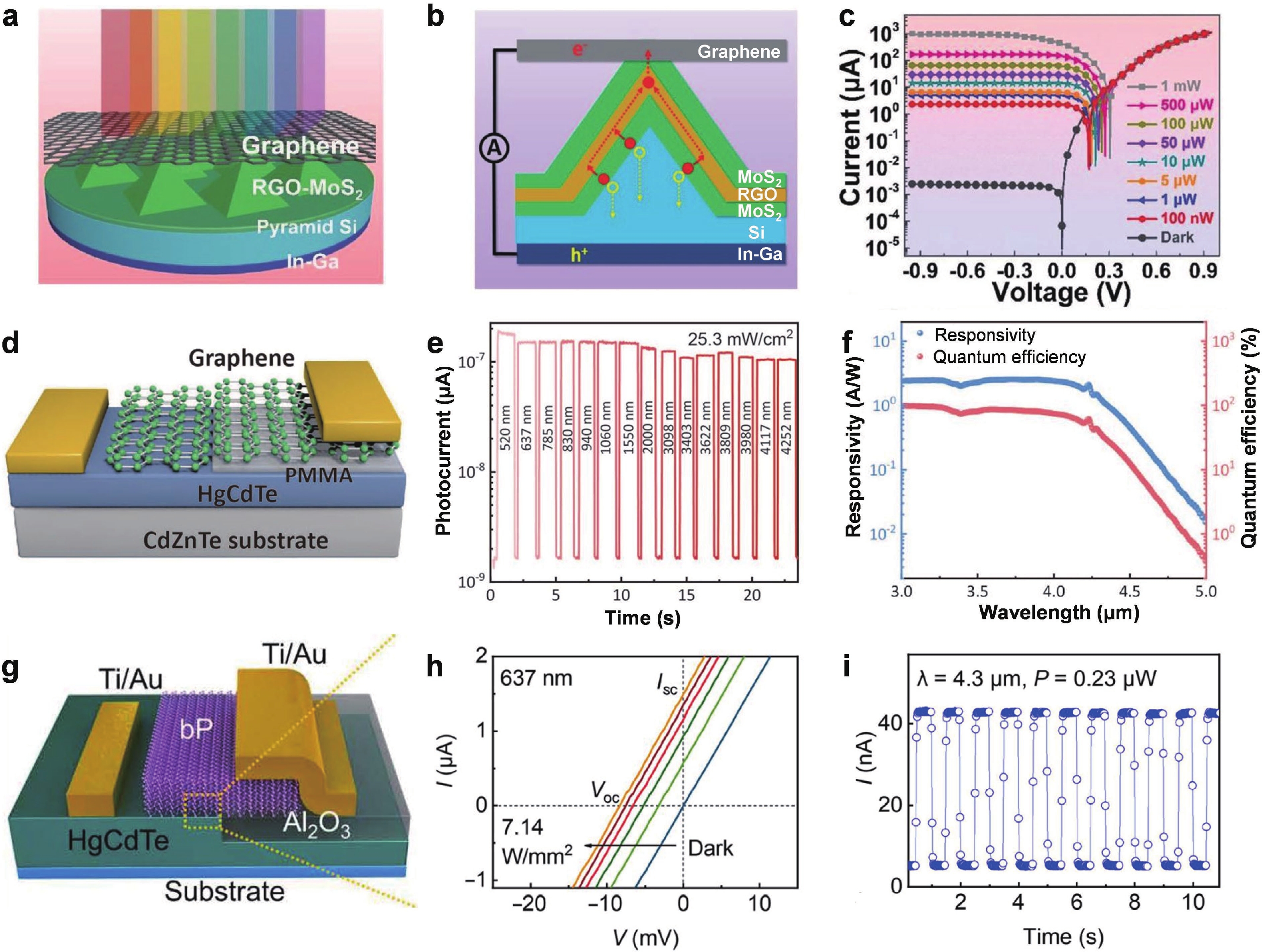
Xiao P, Mao J, Ding K, et al. Solution-processed 3D RGO-MoS 2/pyramid Si heterojunction for ultrahigh detectivity and ultra-broadband photodetection. Adv Mater, 2018, 30, 1801729 doi: 10.1002/adma.201801729 |
| [140] |
Chen W J, Liang R R, Zhang S Q, et al. Ultrahigh sensitive near-infrared photodetectors based on MoTe 2/germanium heterostructure. Nano Res, 2020, 13, 127 doi: 10.1007/s12274-019-2583-5 |
| [141] |
Lei W, Antoszewski J, Faraone L. Progress, challenges, and opportunities for HgCdTe infrared materials and detectors. Appl Phys Rev, 2015, 2, 041303 doi: 10.1063/1.4936577 |
| [142] |
Wang Y, Gu Y, Cui A L, et al. Fast uncooled mid-wavelength infrared photodetectors with heterostructures of van der Waals on epitaxial HgCdTe. Adv Mater, 2022, 34, 2107772 doi: 10.1002/adma.202107772 |
| [143] |
Jiao H X, Wang X D, Chen Y, et al. HgCdTe/black phosphorus van der Waals heterojunction for high-performance polarization-sensitive midwave infrared photodetector. Sci Adv, 2022, 8, eabn1811 doi: 10.1126/sciadv.abn1811 |
| [144] |
Nadupalli S, Kreisel J, Granzow T. Increasing bulk photovoltaic current by strain tuning. Sci Adv, 2019, 5, eaau9199 doi: 10.1126/sciadv.aau9199 |
| [145] |
Kushnir K, Wang M J, Fitzgerald P D, et al. Ultrafast zero-bias photocurrent in GeS nanosheets: promise for photovoltaics. ACS Energy Lett, 2017, 2, 1429 doi: 10.1021/acsenergylett.7b00330 |
| [146] |
Ai H Q, Liu D, Geng J Z, et al. Theoretical evidence of the spin-valley coupling and valley polarization in two-dimensional MoSi 2X 4 (X = N, P, and As). Phys Chem Chem Phys, 2021, 23, 3144 doi: 10.1039/D0CP05926A |
| [147] |
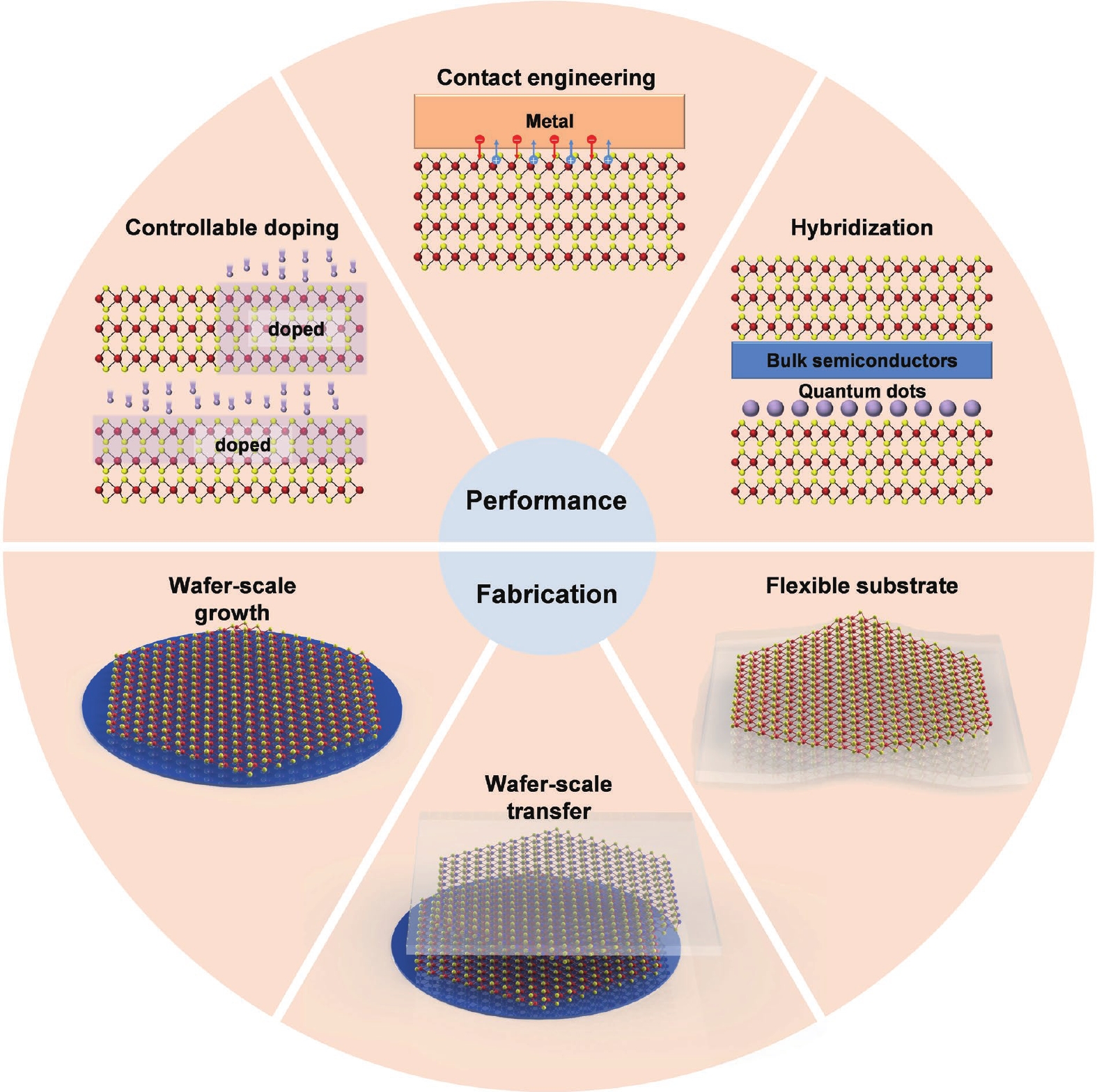
|
| [148] |
Park N G, Segawa H. Research direction toward theoretical efficiency in perovskite solar cells. ACS Photonics, 2018, 5, 2970 doi: 10.1021/acsphotonics.8b00124 |
| [149] |
Rühle S. Tabulated values of the Shockley–Queisser limit for single junction solar cells. Sol Energy, 2016, 130, 139 doi: 10.1016/j.solener.2016.02.015 |
| [150] |
Spanier J E, Fridkin V M, Rappe A M, et al. Power conversion efficiency exceeding the Shockley–Queisser limit in a ferroelectric insulator. Nat Photonics, 2016, 10, 611 doi: 10.1038/nphoton.2016.143 |
| [151] |
Han H, Song S, Lee J H, et al. Switchable photovoltaic effects in hexagonal manganite thin films having narrow band gaps. Chem Mater, 2015, 27, 7425 doi: 10.1021/acs.chemmater.5b03408 |
| [152] |
Bai Y, Jantunen H, Juuti J. Ferroelectric oxides for solar energy conversion, multi-source energy harvesting/sensing, and opto-ferroelectric applications. ChemSusChem, 2019, 12, 2540 doi: 10.1002/cssc.201900671 |
| [153] |
Zhang Y, Holder T, Ishizuka H, et al. Switchable magnetic bulk photovoltaic effect in the two-dimensional magnet CrI 3. Nat Commun, 2019, 10, 3783 doi: 10.1038/s41467-019-11832-3 |
| [154] |
Ding W J, Zhu J B, Wang Z, et al. Prediction of intrinsic two-dimensional ferroelectrics in In 2Se 3 and other III 2-VI 3 van der Waals materials. Nat Commun, 2017, 8, 14956 doi: 10.1038/ncomms14956 |
| [155] |
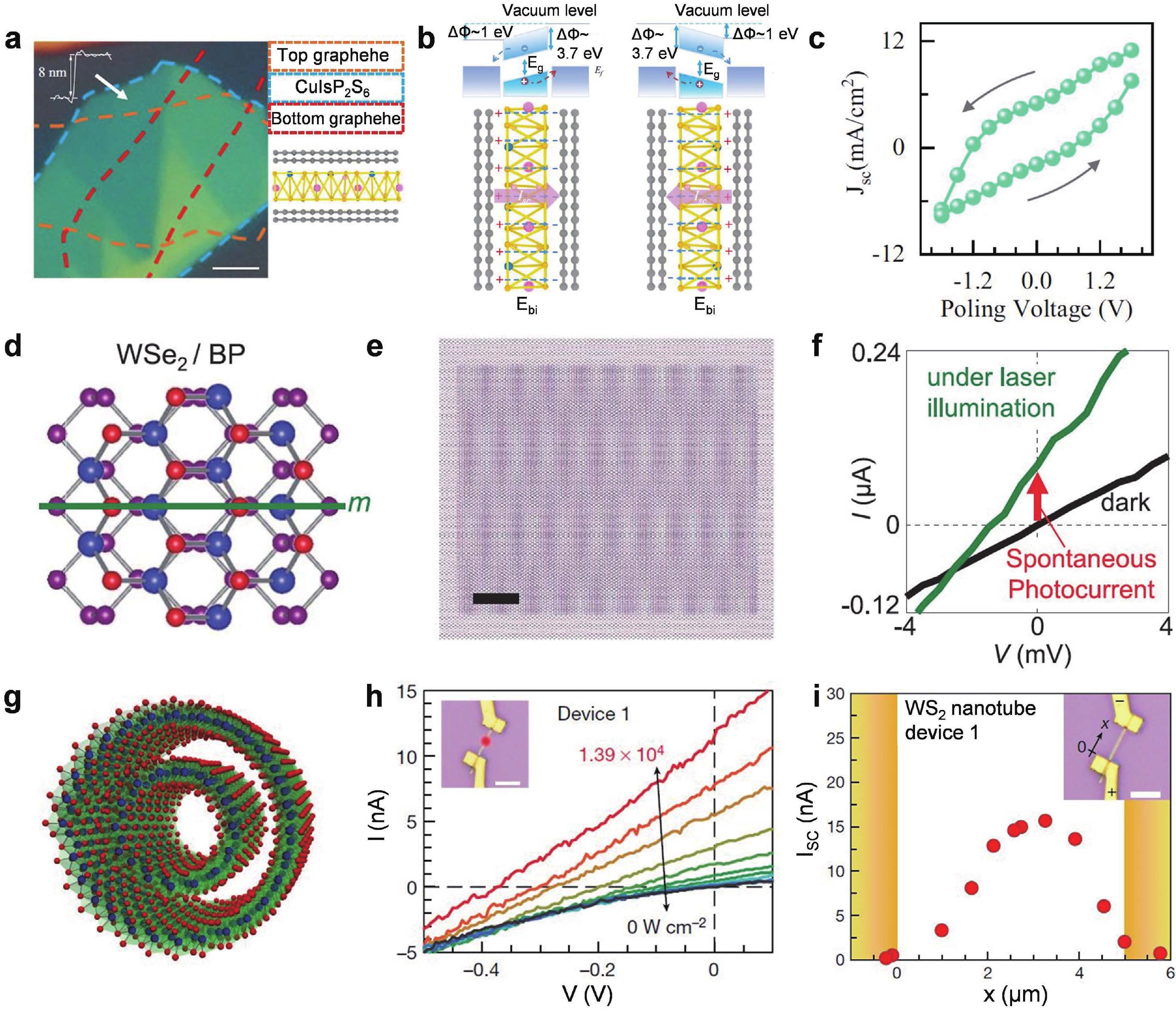
Li Y, Fu J, Mao X Y, et al. Enhanced bulk photovoltaic effect in two-dimensional ferroelectric CuInP 2S 6. Nat Commun, 2021, 12, 5896 doi: 10.1038/s41467-021-26200-3 |
| [156] |
Akamatsu T, Ideue T, Zhou L, et al. A van der Waals interface that creates in-plane polarization and a spontaneous photovoltaic effect. Science, 2021, 372, 68 doi: 10.1126/science.aaz9146 |
| [157] |
Qin F, Shi W, Ideue T, et al. Superconductivity in a chiral nanotube. Nat Commun, 2017, 8, 14465 doi: 10.1038/ncomms14465 |
| [158] |
Yadgarov L, Višić B, Abir T, et al. Strong light-matter interaction in tungsten disulfide nanotubes. Phys Chem Chem Phys, 2018, 20, 20812 doi: 10.1039/C8CP02245C |
| [159] |
Zhang C Y, Wang S, Yang L J, et al. High-performance photodetectors for visible and near-infrared lights based on individual WS 2 nanotubes. Appl Phys Lett, 2012, 100, 243101 doi: 10.1063/1.4729144 |
| [160] |
Jariwala D, Davoyan A R, Wong J, et al. Van der Waals materials for atomically-thin photovoltaics: promise and outlook. ACS Photonics, 2017, 4, 2962 doi: 10.1021/acsphotonics.7b01103 |
| [161] |
Schmidt H, Giustiniano F, Eda G. Electronic transport properties of transition metal dichalcogenide field-effect devices: surface and interface effects. Chem Soc Rev, 2015, 44, 7715 doi: 10.1039/C5CS00275C |
| [162] |
Vu Q A, Yu W J. Electronics and optoelectronics based on two-dimensional materials. J Korean Phys Soc, 2018, 73, 1 doi: 10.3938/jkps.73.1 |
| [163] |
Manzeli S, Ovchinnikov D, Pasquier D, et al. 2D transition metal dichalcogenides. Nat Rev Mater, 2017, 2, 17033 doi: 10.1038/natrevmats.2017.33 |
| [164] |
Lee D H, Lee J J, Kim Y S, et al. Remote modulation doping in van der Waals heterostructure transistors. Nat Electron, 2021, 4, 664 doi: 10.1038/s41928-021-00641-6 |
| [165] |
Li W S, Gong X S, Yu Z H, et al. Approaching the quantum limit in two-dimensional semiconductor contacts. Nature, 2023, 613, 274 doi: 10.1038/s41586-022-05431-4 |
| [166] |
|
| [167] |
Ma K Y, Zhang L N, Jin S, et al. Epitaxial single-crystal hexagonal boron nitride multilayers on Ni (111). Nature, 2022, 606, 88 doi: 10.1038/s41586-022-04745-7 |
| [168] |
Xu X L, Pan Y, Liu S, et al. Seeded 2D epitaxy of large-area single-crystal films of the van der Waals semiconductor 2H MoTe 2. Science, 2021, 372, 195 doi: 10.1126/science.abf5825 |
| [169] |
Yuan G W, Liu W L, Huang X L, et al. Stacking transfer of wafer-scale graphene-based van der Waals superlattices. Nat Commun, 2023, 14, 5457 doi: 10.1038/s41467-023-41296-5 |
| [170] |
Liu G Y, Tian Z A, Yang Z Y, et al. Graphene-assisted metal transfer printing for wafer-scale integration of metal electrodes and two-dimensional materials. Nat Electron, 2022, 5, 275 doi: 10.1038/s41928-022-00764-4 |


 Haoyun Wang received his B.S. degree in functional materials from Huazhong University of Science and Technology (HUST) in Wuhan, China in 2020. Currently, he is pursuing a doctor’s degree in material physics and chemistry from HUST. His current research interest is focused on 2D mateirals based electronic and optoelectronic devices.
 Xingyu Song received her B.S. degree in materials science and engineering from Northeastern University in Shenyang, China in 2021. Currently, she is pursuing a M.S. degree in materials science from Huazhong University of Science and Technology in Wuhan. Her current research interest is focused on 2D materials based tunneling transistors.
 Xing Zhou is a Professor of School of Materials Science and Engineering, Huazhong University of Science and Technology (HUST). He received his B.S degree in inorganic nonmetallic materials from Wuhan University of Science and Technology (WUST) in 2012, and received his Ph.D. from HUST in 2017. His current research interests focus on the controllable synthesis of 2D materials and their heterostructures for optoelectronics.
 Tianyou Zhai received his B.S. degree in chemistry from Zhengzhou University in 2003, and then received Ph.D. degree in physical chemistry from the Institute of Chemistry, Chinese Academy of Sciences (ICCAS) in 2008. Afterward, he joined the National Institute for Materials Science (NIMS) as a JSPS postdoctoral fellow, and then as an ICYS-MANA researcher within NIMS. Currently, he is a Chief Professor of School of Materials Science and Engineering, Huazhong University of Science and Technology (HUST). His research interests include the controlled synthesis and exploration of fundamental physical properties of inorganic functional nanomaterials, as well as their applications in optoelectronics.
 DownLoad: