


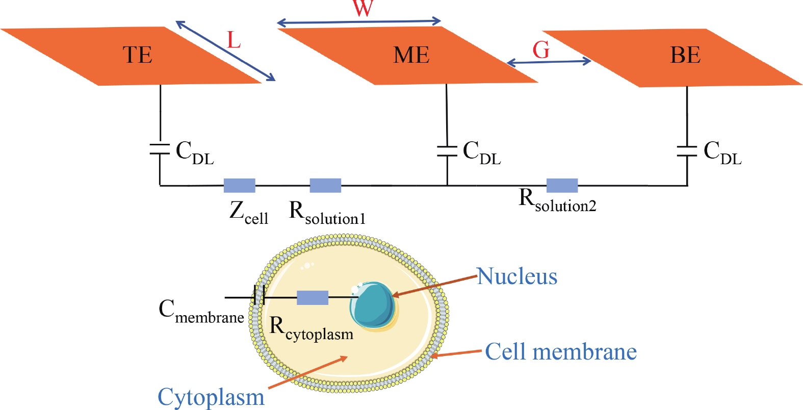
Fig. 1.
(Color online) Schematic of EIS flow cytometry and equivalent circuit model of animal cells.
ARTICLES
Shengxun Cai1, Jianqing Nie1, Kun Wang2, Yimin Guan1, 2 and Demeng Liu1, 2,
Corresponding author: Demeng Liu, demeng_liu@shu.edu.cn
Abstract: Electrochemical impedance spectroscopy (EIS) flow cytometry offers the advantages of speed, affordability, and portability in cell analysis and cytometry applications. However, the integration challenges of microfluidic and EIS read-out circuits hinder the downsizing of cytometry devices. To address this, we developed a thermal-bubble-driven impedance flow cytometric application-specific integrated circuit (ASIC). The thermal-bubble micropump avoids external piping and equipment, enabling high-throughput designs. With a total of 36 cell counting channels, each measuring 884 × 220 μm2, the chip significantly enhances the throughput of flow cytometers. Each cell counting channel incorporates a differential trans-impedance amplifier (TIA) to amplify weak biosensing signals. By eliminating the parasitic parameters created at the complementary metal-oxide-semiconductor transistor (CMOS)-micro-electromechanical systems (MEMS) interface, the counting accuracy can be increased. The on-chip TIA can adjust feedback resistance from 5 to 60 kΩ to accommodate solutions with different impedances. The chip effectively classifies particles of varying sizes, demonstrated by the average peak voltages of 0.0529 and 0.4510 mV for 7 and 14 μm polystyrene beads, respectively. Moreover, the counting accuracies of the chip for polystyrene beads and MSTO-211H cells are both greater than 97.6%. The chip exhibits potential for impedance flow cytometer at low cost, high-throughput, and miniaturization for the application of point-of-care diagnostics.
Keywords: EIS, flow cytometry, CMOS-MEMS, thermal bubble, lab-on-chip
| [1] |
Adan A, Alizada G, Kiraz Y, et al. Flow cytometry: Basic principles and applications. Crit Rev Biotechnol, 2017, 37(2), 163 doi: 10.3109/07388551.2015.1128876
|
| [2] |
Lu N, Tay H M, Petchakup C, et al. Label-free microfluidic cell sorting and detection for rapid blood analysis. Lab Chip, 2023, 23(5), 1226 doi: 10.1039/D2LC00904H
|
| [3] |
McKinnon K M. Flow Cytometry: An Overview, Curr Protoc Immunol, 2018, 120(1), 5 doi: 10.1002/cpim.40
|
| [4] |
Hurley J. Sizing particles with a coulter counter. Biophys J, 1970, 10(1), 74 doi: 10.1016/S0006-3495(70)86286-5
|
| [5] |
Don M. The coulter principle: Foundation of an industry. JALA J Assoc Lab Autom, 2003, 8(6), 72 doi: 10.1016/S1535-5535-03-00023-6
|
| [6] |
Rodriguez-Trujillo R, Mills C A, Samitier J, et al. Low cost micro-Coulter counter with hydrodynamic focusing. Microfluid Nanofluid, 2007, 3(2), 171 doi: 10.1007/s10404-006-0113-8
|
| [7] |
He Z, Mansfeld F. Exploring the use of electrochemical impedance spectroscopy (EIS) in microbial fuel cell studies. Energy Environ Sci, 2009, 2(2), 215 doi: 10.1039/B814914C
|
| [8] |
Pastor-Fernández C, Dhammika W W, Marco J, et al. Identification and quantification of ageing mechanisms in lithium-ion batteries using the EIS technique. 2016 IEEE Transportation Electrification Conference and Expo (ITEC), 2016, 1 doi: 10.1109/ITEC.2016.7520198
|
| [9] |
Giagkoulovits C, Cheah B C, Al-Rawhani M A, et al. A 16 x 16 CMOS amperometric microelectrode array for simultaneous electrochemical measurements. IEEE Trans Circuits Syst I Regul Pap, 2018, 65(9), 2821 doi: 10.1109/TCSI.2018.2794502
|
| [10] |
Xu J W, Hong Z L. Low power bio-impedance sensor interfaces: Review and electronics design methodology. IEEE Rev Biomed Eng, 2022, 15, 23 doi: 10.1109/RBME.2020.3041053
|
| [11] |
Bounik R, Cardes F, Ulusan H, et al. Impedance imaging of cells and tissues: Design and applications. BME Front, 2022, 2022, 1 doi: 10.34133/2022/9857485
|
| [12] |
Park J Y, Park S M. DNA hybridization sensors based on electrochemical impedance spectroscopy as a detection tool. Sensors, 2009, 9(12), 9513 doi: 10.3390/s91209513
|
| [13] |
Bernabini C, Holmes D, Morgan H. Micro-impedance cytometry for detection and analysis of micron-sized particles and bacteria. Lab Chip, 2011, 11(3), 407 doi: 10.1039/C0LC00099J
|
| [14] |
Cheung K, Gawad S, Renaud P. Impedance spectroscopy flow cytometry: On-chip label-free cell differentiation. Cytometry Pt A, 2005, 65A(2), 124 doi: 10.1002/cyto.a.20141
|
| [15] |
Honrado C, Bisegna P, Swami N S, et al. Single-cell microfluidic impedance cytometry: From raw signals to cell phenotypes using data analytics. Lab Chip, 2021, 21(1), 22 doi: 10.1039/D0LC00840K
|
| [16] |
Haandbæk N, With O, Bürgel S C, et al. Resonance-enhanced microfluidic impedance cytometer for detection of single bacteria. Lab Chip, 2014, 14(17), 3313 doi: 10.1039/C4LC00576G
|
| [17] |
Nguyen T H, Nguyen H A, Tran Thi Y V, et al. Concepts, electrode configuration, characterization, and data analytics of electric and electrochemical microfluidic platforms: A review. Analyst, 2023, 148(9), 1912 doi: 10.1039/D2AN02027K
|
| [18] |
van Berkel C, Gwyer J D, Deane S, et al. Integrated systems for rapid point of care (PoC) blood cell analysis. Lab Chip, 2011, 11(7), 1249 doi: 10.1039/c0lc00587h
|
| [19] |
Sun D P, Lu J, Chen Z G. Microfluidic contactless conductivity cytometer for electrical cell sensing and counting. RSC Adv, 2015, 5(73), 59306 doi: 10.1039/C5RA08371K
|
| [20] |
Yang X P, Wang K, Huang P, et al. Thermal bubble-driven impedance-based high-throughput cell counting chip design. AIP Adv, 2023, 13(6), 065308. doi: 10.1063/5.0153846
|
| [21] |
Hassan U, Reddy B Jr, Damhorst G, et al. A microfluidic biochip for complete blood cell counts at the point-of-care. TECHNOLOGY, 2015, 3(4), 201 doi: 10.1142/S2339547815500090
|
| [22] |
Zhong J W, Liang M H, Ai Y. Submicron-precision particle characterization in microfluidic impedance cytometry with double differential electrodes. Lab Chip, 2021, 21(15), 2869 doi: 10.1039/D1LC00481F
|
| [23] |
Shen B Y, Dawes J, Johnston M L. A 10 MΩ, 50 kHz-40 MHz impedance measurement architecture for source-differential flow cytometry. IEEE Trans Biomed Circuits Syst, 2022, 16(5), 766 doi: 10.1109/TBCAS.2022.3182905
|
| [24] |
Iyer V, Issadore D A, Aflatouni F. The next generation of hybrid microfluidic/integrated circuit chips: Recent and upcoming advances in high-speed, high-throughput, and multifunctional lab-on-IC systems. Lab Chip, 2023, 23(11), 2553 doi: 10.1039/D2LC01163H
|
| [25] |
Carminati M, Gervasoni G, Sampietro M, et al. Note: Differential configurations for the mitigation of slow fluctuations limiting the resolution of digital lock-in amplifiers. Rev Sci Instrum, 2016, 87(2), 026102 doi: 10.1063/1.4941721
|
| [26] |
Sharma N, Kumar M, Kumari N, et al. Tantalum oxide thin films for electrochemical pH sensor. Mater Res Express, 2020, 7(3), 036405 doi: 10.1088/2053-1591/ab7ced
|
| [27] |
Carminati M, Ferrari G, Vahey M D, et al. Miniaturized impedance flow cytometer: Design rules and integrated readout. IEEE Trans Biomed Circuits Syst, 2017, 11, 1438 doi: 10.1109/TBCAS.2017.2748158
|
| [28] |
Lee K H, Nam J, Choi S, et al. A CMOS impedance cytometer for 3D flowing single-cell real-time analysis with ΔΣ error correction. 2012 IEEE International Solid-State Circuits Conference, 2012, 304 doi: 10.1109/ISSCC.2012.6177024
|
| [29] |
Fu Y S, Yuan Q B, Guo J H. Lab-on-PCB-based micro-cytometer for circulating tumor cells detection and enumeration. Microfluid Nanofluid, 2017, 21(2), 20 doi: 10.1007/s10404-017-1854-2
|
| [30] |
Chien J C, Ameri A, Yeh E C, et al. A high-throughput flow cytometry-on-a-CMOS platform for single-cell dielectric spectroscopy at microwave frequencies. Lab Chip, 2018, 18(14), 2065 doi: 10.1039/C8LC00299A
|
| [31] |
Feng Y X, Zhu J W, Chai H C, et al. Impedance-based multimodal electrical-mechanical intrinsic flow cytometry. Small, 2023, 19(45), 2370379 doi: 10.1002/smll.202370379
|
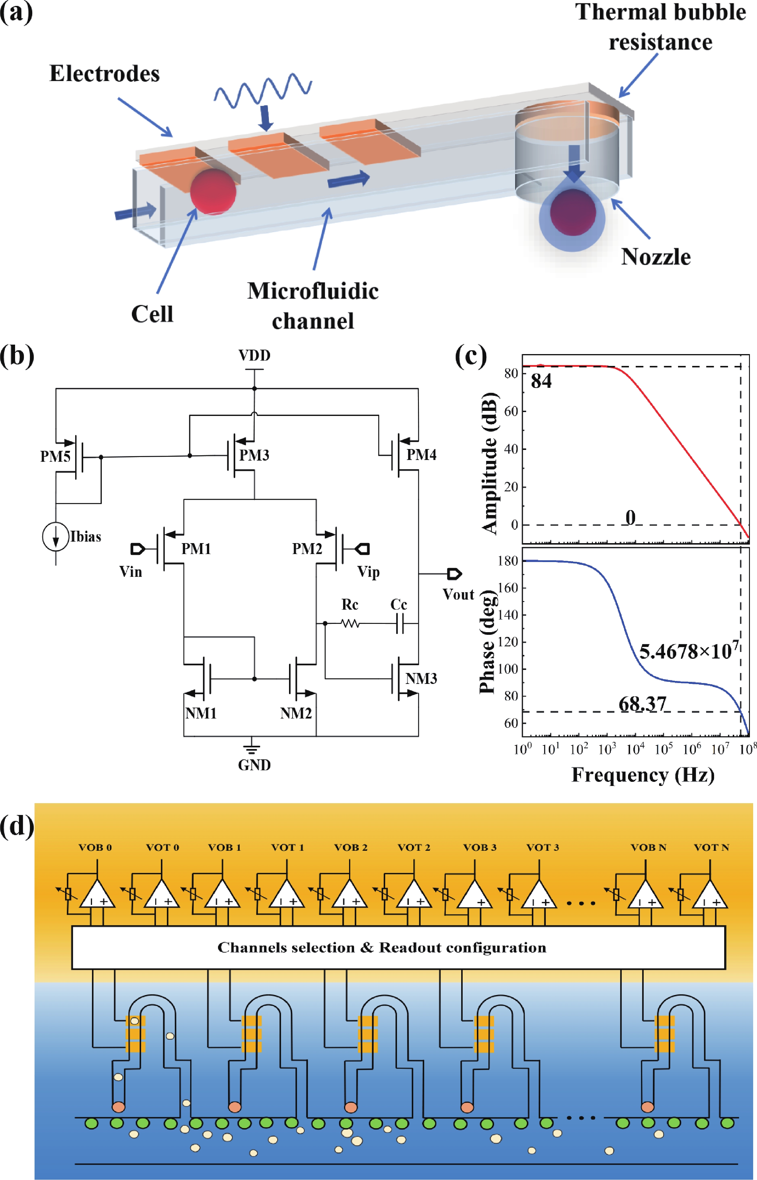
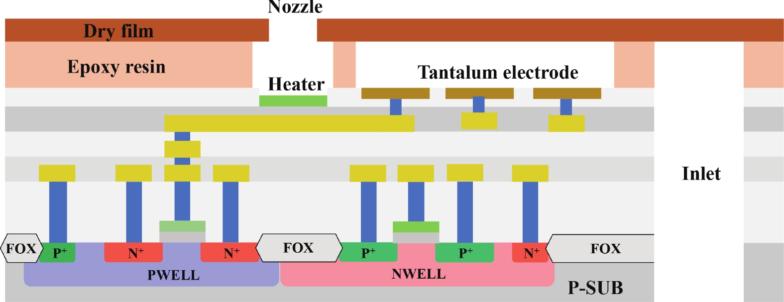
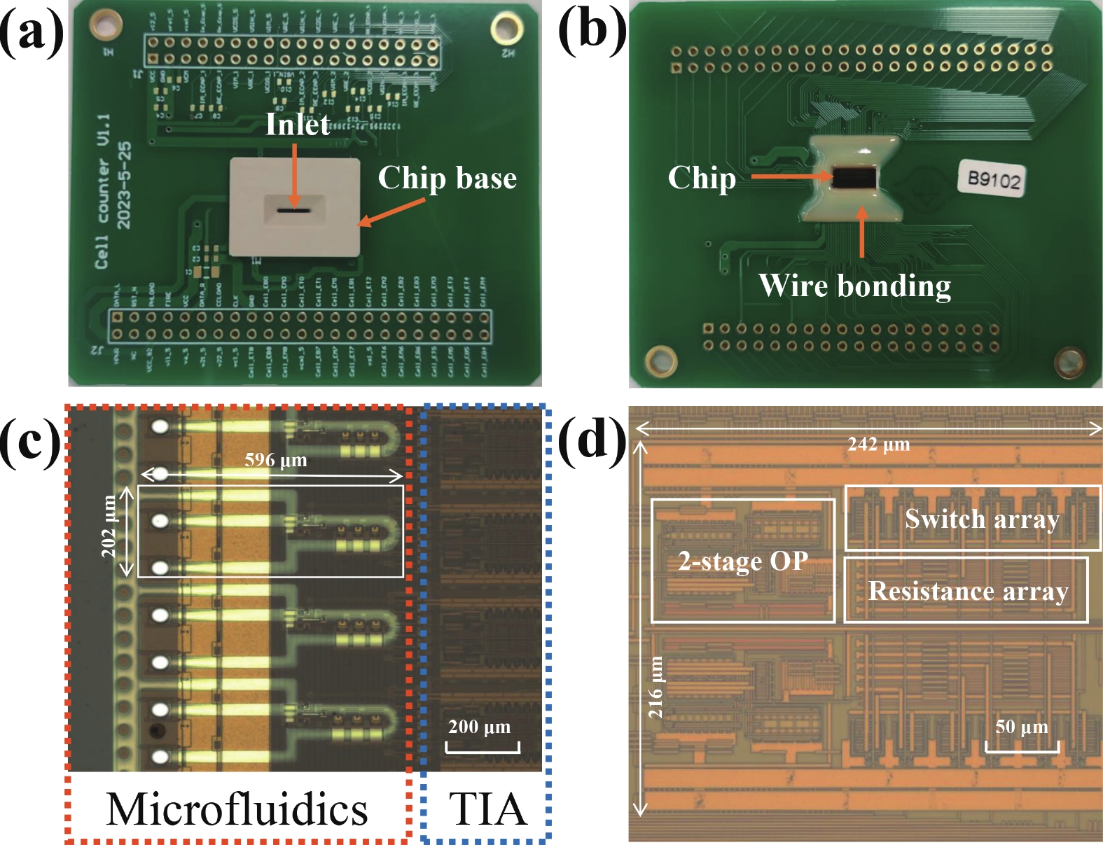
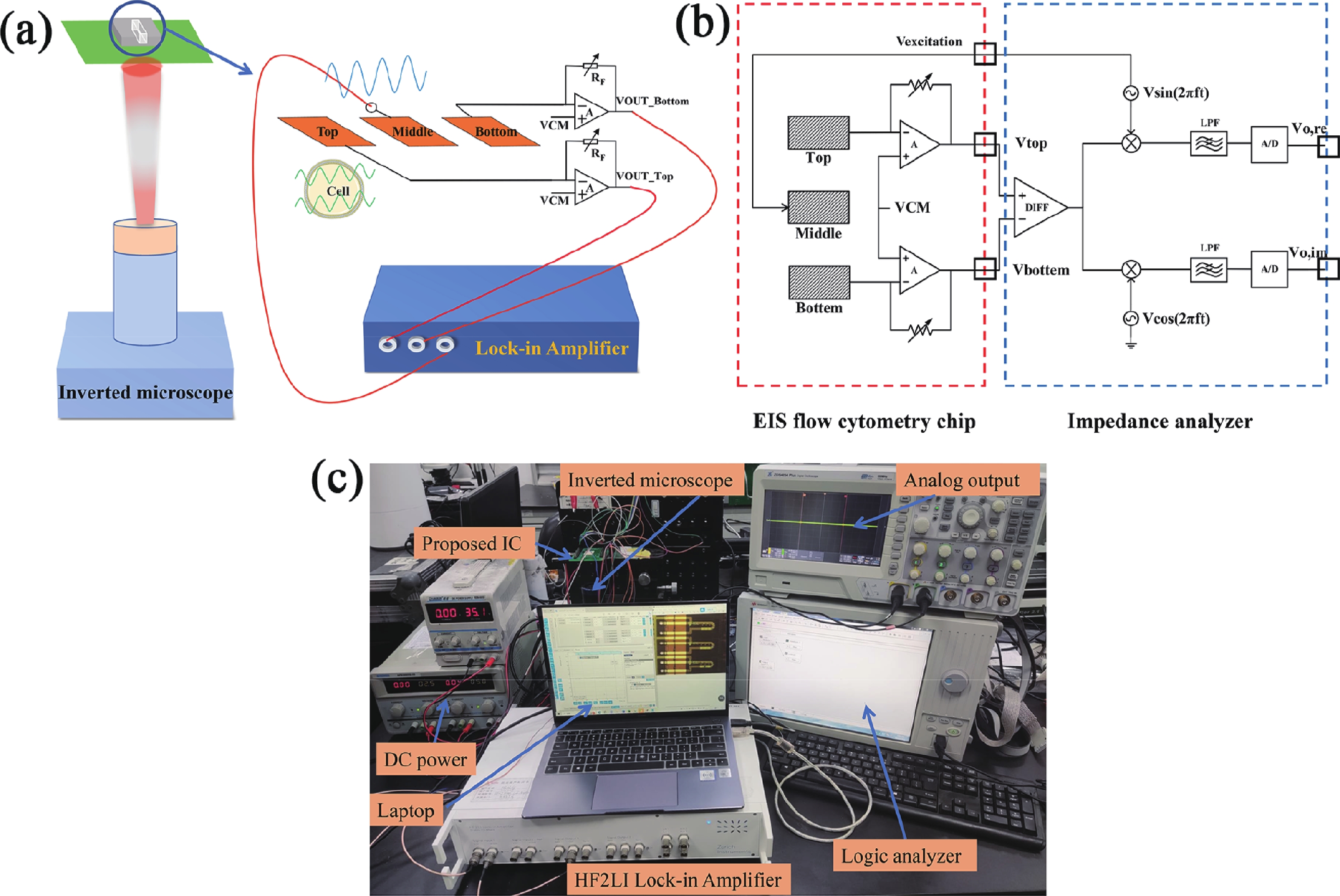
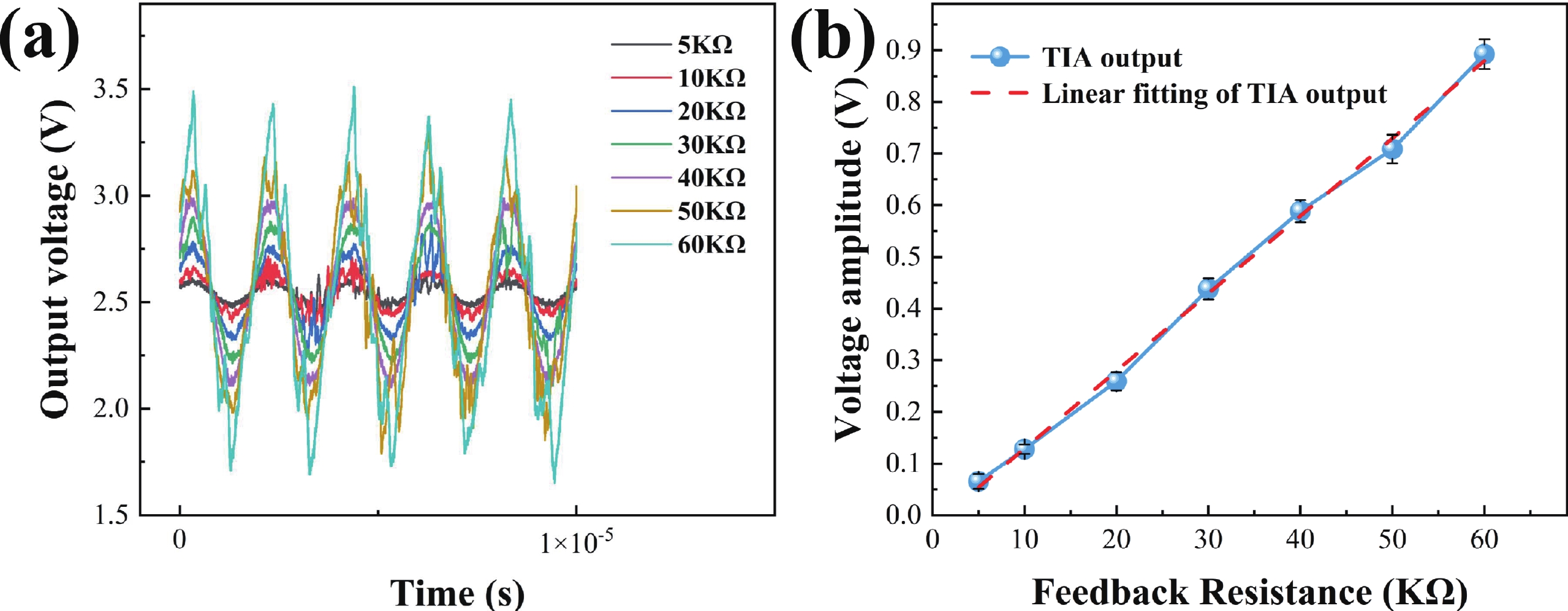
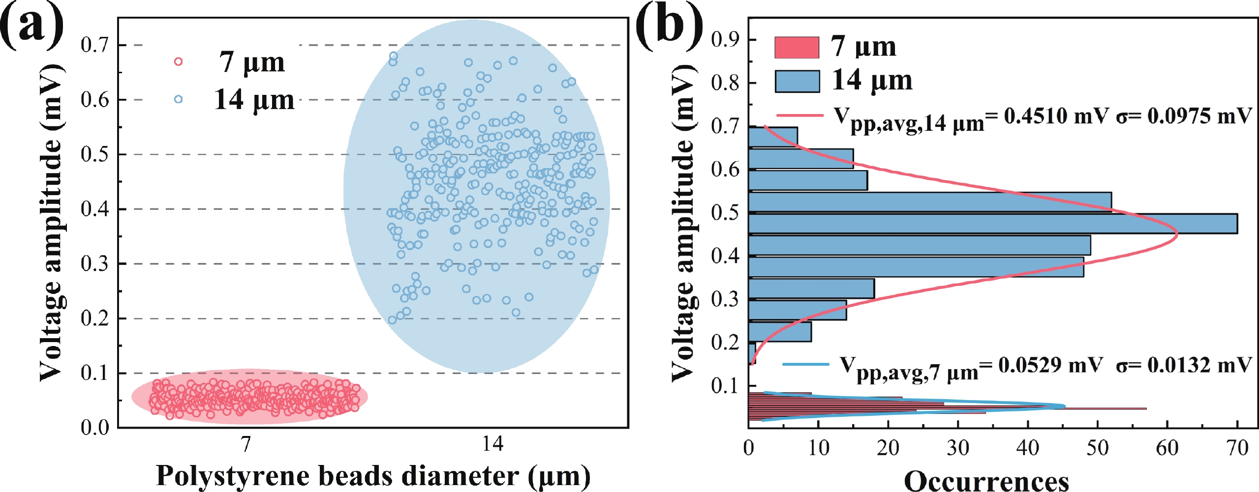
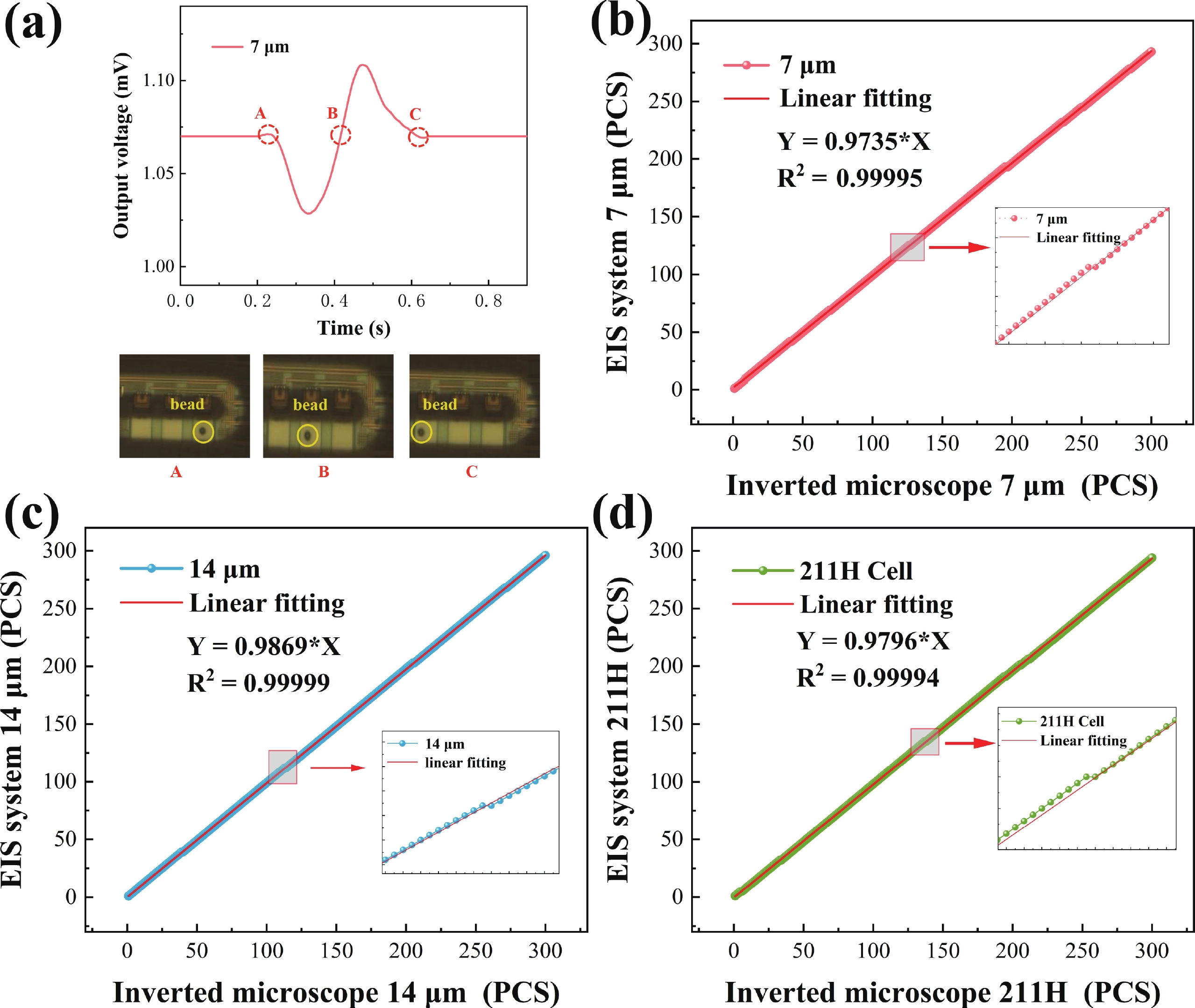
Table 1. Accuracy of detection of different types of particles.
| Particle types | Number of inverted microscope observation particles (pcs) | Number of signals measured by EIS analyzer (pcs) | Detection accuracy (%) |
| 7 μm polystyrene beads | 300 | 293 | 97.66 |
| 14 μm polystyrene beads | 300 | 296 | 98.66 |
| 211H cells | 300 | 294 | 98.0 |
 DownLoad: CSV
Table 2. Performance comparison of impedance flow cytometers.
| First author (year) | Signal readout method | Drive type | Number of detection channels | Device size | Cell measurement | Coefficient of determination (R2) | Throughput | Ref |
| This work | On-chip TIA + lock-in amplifier | Thermal bubble micropump | 36 | 24 mm2 | MSTO-211H | 0.999 | 16 200 cells/s | − |
| Liu et al. (2023) | Lock-in amplifier | Thermal bubble micropump | 100 | 38 mm2 | MSTO-211H | 0.999 | 45 000 cells/s | [20] |
| Sun et al. (2015) | Lock-in amplifier | Syringe pump | 1 | 21 cm2 | MCF-7, HCM | 0.984 | 60 cells/min | [19] |
| Carminati et al. (2017) | Lock-in amplifier | Syringe pump | 2 | 46 cm2 | Yeast cells | − | 2000 cells/s | [27] |
| Lee et al. (2012) | Discrete IC | Syringe pump | 1 | − | RBC | − | 267 cells/s | [28] |
| Fu et al. (2017) | Lock-in amplifier | Syringe pump | 1 | − | RBC, WBC, CTC | 0.992 | − | [29] |
| Johnston et al. (2022) | Discrete IC | Syringe pump | 1 | 0.28 mm2 | − | − | 1 cells/s | [23] |
| Niknejad et al. (2018) | Discrete IC | Syringe pump | 1 | − | THP-1, MDA-MB-231 | − | 1000 cells/s | [30] |
| Wang et al. (2023) | Lock-in amplifier | Syringe pump | 1 | − | MDA-MB-468 | − | 500 cells/min | [31] |
DownLoad: CSV
| [1] |
Adan A, Alizada G, Kiraz Y, et al. Flow cytometry: Basic principles and applications. Crit Rev Biotechnol, 2017, 37(2), 163 doi: 10.3109/07388551.2015.1128876
|
| [2] |
Lu N, Tay H M, Petchakup C, et al. Label-free microfluidic cell sorting and detection for rapid blood analysis. Lab Chip, 2023, 23(5), 1226 doi: 10.1039/D2LC00904H
|
| [3] |
McKinnon K M. Flow Cytometry: An Overview, Curr Protoc Immunol, 2018, 120(1), 5 doi: 10.1002/cpim.40
|
| [4] |
Hurley J. Sizing particles with a coulter counter. Biophys J, 1970, 10(1), 74 doi: 10.1016/S0006-3495(70)86286-5
|
| [5] |
Don M. The coulter principle: Foundation of an industry. JALA J Assoc Lab Autom, 2003, 8(6), 72 doi: 10.1016/S1535-5535-03-00023-6
|
| [6] |
Rodriguez-Trujillo R, Mills C A, Samitier J, et al. Low cost micro-Coulter counter with hydrodynamic focusing. Microfluid Nanofluid, 2007, 3(2), 171 doi: 10.1007/s10404-006-0113-8
|
| [7] |
He Z, Mansfeld F. Exploring the use of electrochemical impedance spectroscopy (EIS) in microbial fuel cell studies. Energy Environ Sci, 2009, 2(2), 215 doi: 10.1039/B814914C
|
| [8] |
Pastor-Fernández C, Dhammika W W, Marco J, et al. Identification and quantification of ageing mechanisms in lithium-ion batteries using the EIS technique. 2016 IEEE Transportation Electrification Conference and Expo (ITEC), 2016, 1 doi: 10.1109/ITEC.2016.7520198
|
| [9] |
Giagkoulovits C, Cheah B C, Al-Rawhani M A, et al. A 16 x 16 CMOS amperometric microelectrode array for simultaneous electrochemical measurements. IEEE Trans Circuits Syst I Regul Pap, 2018, 65(9), 2821 doi: 10.1109/TCSI.2018.2794502
|
| [10] |
Xu J W, Hong Z L. Low power bio-impedance sensor interfaces: Review and electronics design methodology. IEEE Rev Biomed Eng, 2022, 15, 23 doi: 10.1109/RBME.2020.3041053
|
| [11] |
Bounik R, Cardes F, Ulusan H, et al. Impedance imaging of cells and tissues: Design and applications. BME Front, 2022, 2022, 1 doi: 10.34133/2022/9857485
|
| [12] |
Park J Y, Park S M. DNA hybridization sensors based on electrochemical impedance spectroscopy as a detection tool. Sensors, 2009, 9(12), 9513 doi: 10.3390/s91209513
|
| [13] |
Bernabini C, Holmes D, Morgan H. Micro-impedance cytometry for detection and analysis of micron-sized particles and bacteria. Lab Chip, 2011, 11(3), 407 doi: 10.1039/C0LC00099J
|
| [14] |
Cheung K, Gawad S, Renaud P. Impedance spectroscopy flow cytometry: On-chip label-free cell differentiation. Cytometry Pt A, 2005, 65A(2), 124 doi: 10.1002/cyto.a.20141
|
| [15] |
Honrado C, Bisegna P, Swami N S, et al. Single-cell microfluidic impedance cytometry: From raw signals to cell phenotypes using data analytics. Lab Chip, 2021, 21(1), 22 doi: 10.1039/D0LC00840K
|
| [16] |
Haandbæk N, With O, Bürgel S C, et al. Resonance-enhanced microfluidic impedance cytometer for detection of single bacteria. Lab Chip, 2014, 14(17), 3313 doi: 10.1039/C4LC00576G
|
| [17] |
Nguyen T H, Nguyen H A, Tran Thi Y V, et al. Concepts, electrode configuration, characterization, and data analytics of electric and electrochemical microfluidic platforms: A review. Analyst, 2023, 148(9), 1912 doi: 10.1039/D2AN02027K
|
| [18] |
van Berkel C, Gwyer J D, Deane S, et al. Integrated systems for rapid point of care (PoC) blood cell analysis. Lab Chip, 2011, 11(7), 1249 doi: 10.1039/c0lc00587h
|
| [19] |
Sun D P, Lu J, Chen Z G. Microfluidic contactless conductivity cytometer for electrical cell sensing and counting. RSC Adv, 2015, 5(73), 59306 doi: 10.1039/C5RA08371K
|
| [20] |
Yang X P, Wang K, Huang P, et al. Thermal bubble-driven impedance-based high-throughput cell counting chip design. AIP Adv, 2023, 13(6), 065308. doi: 10.1063/5.0153846
|
| [21] |
Hassan U, Reddy B Jr, Damhorst G, et al. A microfluidic biochip for complete blood cell counts at the point-of-care. TECHNOLOGY, 2015, 3(4), 201 doi: 10.1142/S2339547815500090
|
| [22] |
Zhong J W, Liang M H, Ai Y. Submicron-precision particle characterization in microfluidic impedance cytometry with double differential electrodes. Lab Chip, 2021, 21(15), 2869 doi: 10.1039/D1LC00481F
|
| [23] |
Shen B Y, Dawes J, Johnston M L. A 10 MΩ, 50 kHz-40 MHz impedance measurement architecture for source-differential flow cytometry. IEEE Trans Biomed Circuits Syst, 2022, 16(5), 766 doi: 10.1109/TBCAS.2022.3182905
|
| [24] |
Iyer V, Issadore D A, Aflatouni F. The next generation of hybrid microfluidic/integrated circuit chips: Recent and upcoming advances in high-speed, high-throughput, and multifunctional lab-on-IC systems. Lab Chip, 2023, 23(11), 2553 doi: 10.1039/D2LC01163H
|
| [25] |
Carminati M, Gervasoni G, Sampietro M, et al. Note: Differential configurations for the mitigation of slow fluctuations limiting the resolution of digital lock-in amplifiers. Rev Sci Instrum, 2016, 87(2), 026102 doi: 10.1063/1.4941721
|
| [26] |
Sharma N, Kumar M, Kumari N, et al. Tantalum oxide thin films for electrochemical pH sensor. Mater Res Express, 2020, 7(3), 036405 doi: 10.1088/2053-1591/ab7ced
|
| [27] |
Carminati M, Ferrari G, Vahey M D, et al. Miniaturized impedance flow cytometer: Design rules and integrated readout. IEEE Trans Biomed Circuits Syst, 2017, 11, 1438 doi: 10.1109/TBCAS.2017.2748158
|
| [28] |
Lee K H, Nam J, Choi S, et al. A CMOS impedance cytometer for 3D flowing single-cell real-time analysis with ΔΣ error correction. 2012 IEEE International Solid-State Circuits Conference, 2012, 304 doi: 10.1109/ISSCC.2012.6177024
|
| [29] |
Fu Y S, Yuan Q B, Guo J H. Lab-on-PCB-based micro-cytometer for circulating tumor cells detection and enumeration. Microfluid Nanofluid, 2017, 21(2), 20 doi: 10.1007/s10404-017-1854-2
|
| [30] |
Chien J C, Ameri A, Yeh E C, et al. A high-throughput flow cytometry-on-a-CMOS platform for single-cell dielectric spectroscopy at microwave frequencies. Lab Chip, 2018, 18(14), 2065 doi: 10.1039/C8LC00299A
|
| [31] |
Feng Y X, Zhu J W, Chai H C, et al. Impedance-based multimodal electrical-mechanical intrinsic flow cytometry. Small, 2023, 19(45), 2370379 doi: 10.1002/smll.202370379
|


Article views: 1633 Times PDF downloads: 100 Times Cited by: 0 Times
Received: 23 November 2023 Revised: 04 January 2024 Online: Accepted Manuscript: 22 January 2024Uncorrected proof: 01 February 2024Published: 10 May 2024
| Citation: |
Shengxun Cai, Jianqing Nie, Kun Wang, Yimin Guan, Demeng Liu. A multichannel thermal bubble-actuated impedance flow cytometer with on-chip TIA based on CMOS-MEMS[J]. Journal of Semiconductors, 2024, 45(5): 052201. doi: 10.1088/1674-4926/45/5/052201
****
S X Cai, J Q Nie, K Wang, Y M Guan, and D M Liu, A multichannel thermal bubble-actuated impedance flow cytometer with on-chip TIA based on CMOS-MEMS[J]. J. Semicond., 2024, 45(5), 052201 doi: 10.1088/1674-4926/45/5/052201

|
 Shengxun Cai received his B.Eng. degree from Qingdao University, he is currently a postgraduate student at the School of Microelectronics, Shanghai University. His research interests are intelligent microfluidic and analog integrated circuit design
 Jianqing Nie received his B.Eng. degree from Xi'an Jiaotong University, he is now a postgraduate student at the School of Microelectronics, Shanghai University. His research focuses on the integration of analog front-end integrated circuit design with MEMS arrays
 Kun Wang received his Ph.D. degree from Shanghai Institute of Microsystem and Information Technology, Chinese Academy of Sciences in 2019. He is now a microfluidic engineer at Shanghai AURE Technology Co., LTD. He is working on integration of inkjet printing and biomedicine
 Yimin Guan received his Ph.D. degree from Auburn University in1998. He is currently the co-tutor of the School of Microelectronics at Shanghai University and the CEO of Shanghai AURE Technology Co., LTD. His research focuses on intelligent microfluidic chips based on special application integrated circuit (ASIC) and micromotor system (MEMS) technologies
 Demeng Liu received his Ph.D. degree from Shanghai Institute of Advanced Study, Chinese Academy of Sciences in 2014. He is now a joint tutor at the School of Microelectronics of Shanghai University and an integrated circuit design engineer at Shanghai AURE Technology Co., LTD, for development of intelligent microfluidic chip based on CMOS-MEMS process
| [1] |
Adan A, Alizada G, Kiraz Y, et al. Flow cytometry: Basic principles and applications. Crit Rev Biotechnol, 2017, 37(2), 163 doi: 10.3109/07388551.2015.1128876
|
| [2] |
Lu N, Tay H M, Petchakup C, et al. Label-free microfluidic cell sorting and detection for rapid blood analysis. Lab Chip, 2023, 23(5), 1226 doi: 10.1039/D2LC00904H
|
| [3] |
McKinnon K M. Flow Cytometry: An Overview, Curr Protoc Immunol, 2018, 120(1), 5 doi: 10.1002/cpim.40
|
| [4] |
Hurley J. Sizing particles with a coulter counter. Biophys J, 1970, 10(1), 74 doi: 10.1016/S0006-3495(70)86286-5
|
| [5] |
Don M. The coulter principle: Foundation of an industry. JALA J Assoc Lab Autom, 2003, 8(6), 72 doi: 10.1016/S1535-5535-03-00023-6
|
| [6] |
Rodriguez-Trujillo R, Mills C A, Samitier J, et al. Low cost micro-Coulter counter with hydrodynamic focusing. Microfluid Nanofluid, 2007, 3(2), 171 doi: 10.1007/s10404-006-0113-8
|
| [7] |
He Z, Mansfeld F. Exploring the use of electrochemical impedance spectroscopy (EIS) in microbial fuel cell studies. Energy Environ Sci, 2009, 2(2), 215 doi: 10.1039/B814914C
|
| [8] |
Pastor-Fernández C, Dhammika W W, Marco J, et al. Identification and quantification of ageing mechanisms in lithium-ion batteries using the EIS technique. 2016 IEEE Transportation Electrification Conference and Expo (ITEC), 2016, 1 doi: 10.1109/ITEC.2016.7520198
|
| [9] |
Giagkoulovits C, Cheah B C, Al-Rawhani M A, et al. A 16 x 16 CMOS amperometric microelectrode array for simultaneous electrochemical measurements. IEEE Trans Circuits Syst I Regul Pap, 2018, 65(9), 2821 doi: 10.1109/TCSI.2018.2794502
|
| [10] |
Xu J W, Hong Z L. Low power bio-impedance sensor interfaces: Review and electronics design methodology. IEEE Rev Biomed Eng, 2022, 15, 23 doi: 10.1109/RBME.2020.3041053
|
| [11] |
Bounik R, Cardes F, Ulusan H, et al. Impedance imaging of cells and tissues: Design and applications. BME Front, 2022, 2022, 1 doi: 10.34133/2022/9857485
|
| [12] |
Park J Y, Park S M. DNA hybridization sensors based on electrochemical impedance spectroscopy as a detection tool. Sensors, 2009, 9(12), 9513 doi: 10.3390/s91209513
|
| [13] |
Bernabini C, Holmes D, Morgan H. Micro-impedance cytometry for detection and analysis of micron-sized particles and bacteria. Lab Chip, 2011, 11(3), 407 doi: 10.1039/C0LC00099J
|
| [14] |
Cheung K, Gawad S, Renaud P. Impedance spectroscopy flow cytometry: On-chip label-free cell differentiation. Cytometry Pt A, 2005, 65A(2), 124 doi: 10.1002/cyto.a.20141
|
| [15] |
Honrado C, Bisegna P, Swami N S, et al. Single-cell microfluidic impedance cytometry: From raw signals to cell phenotypes using data analytics. Lab Chip, 2021, 21(1), 22 doi: 10.1039/D0LC00840K
|
| [16] |
Haandbæk N, With O, Bürgel S C, et al. Resonance-enhanced microfluidic impedance cytometer for detection of single bacteria. Lab Chip, 2014, 14(17), 3313 doi: 10.1039/C4LC00576G
|
| [17] |
Nguyen T H, Nguyen H A, Tran Thi Y V, et al. Concepts, electrode configuration, characterization, and data analytics of electric and electrochemical microfluidic platforms: A review. Analyst, 2023, 148(9), 1912 doi: 10.1039/D2AN02027K
|
| [18] |
van Berkel C, Gwyer J D, Deane S, et al. Integrated systems for rapid point of care (PoC) blood cell analysis. Lab Chip, 2011, 11(7), 1249 doi: 10.1039/c0lc00587h
|
| [19] |
Sun D P, Lu J, Chen Z G. Microfluidic contactless conductivity cytometer for electrical cell sensing and counting. RSC Adv, 2015, 5(73), 59306 doi: 10.1039/C5RA08371K
|
| [20] |
Yang X P, Wang K, Huang P, et al. Thermal bubble-driven impedance-based high-throughput cell counting chip design. AIP Adv, 2023, 13(6), 065308. doi: 10.1063/5.0153846
|
| [21] |
Hassan U, Reddy B Jr, Damhorst G, et al. A microfluidic biochip for complete blood cell counts at the point-of-care. TECHNOLOGY, 2015, 3(4), 201 doi: 10.1142/S2339547815500090
|
| [22] |
Zhong J W, Liang M H, Ai Y. Submicron-precision particle characterization in microfluidic impedance cytometry with double differential electrodes. Lab Chip, 2021, 21(15), 2869 doi: 10.1039/D1LC00481F
|
| [23] |
Shen B Y, Dawes J, Johnston M L. A 10 MΩ, 50 kHz-40 MHz impedance measurement architecture for source-differential flow cytometry. IEEE Trans Biomed Circuits Syst, 2022, 16(5), 766 doi: 10.1109/TBCAS.2022.3182905
|
| [24] |
Iyer V, Issadore D A, Aflatouni F. The next generation of hybrid microfluidic/integrated circuit chips: Recent and upcoming advances in high-speed, high-throughput, and multifunctional lab-on-IC systems. Lab Chip, 2023, 23(11), 2553 doi: 10.1039/D2LC01163H
|
| [25] |
Carminati M, Gervasoni G, Sampietro M, et al. Note: Differential configurations for the mitigation of slow fluctuations limiting the resolution of digital lock-in amplifiers. Rev Sci Instrum, 2016, 87(2), 026102 doi: 10.1063/1.4941721
|
| [26] |
Sharma N, Kumar M, Kumari N, et al. Tantalum oxide thin films for electrochemical pH sensor. Mater Res Express, 2020, 7(3), 036405 doi: 10.1088/2053-1591/ab7ced
|
| [27] |
Carminati M, Ferrari G, Vahey M D, et al. Miniaturized impedance flow cytometer: Design rules and integrated readout. IEEE Trans Biomed Circuits Syst, 2017, 11, 1438 doi: 10.1109/TBCAS.2017.2748158
|
| [28] |
Lee K H, Nam J, Choi S, et al. A CMOS impedance cytometer for 3D flowing single-cell real-time analysis with ΔΣ error correction. 2012 IEEE International Solid-State Circuits Conference, 2012, 304 doi: 10.1109/ISSCC.2012.6177024
|
| [29] |
Fu Y S, Yuan Q B, Guo J H. Lab-on-PCB-based micro-cytometer for circulating tumor cells detection and enumeration. Microfluid Nanofluid, 2017, 21(2), 20 doi: 10.1007/s10404-017-1854-2
|
| [30] |
Chien J C, Ameri A, Yeh E C, et al. A high-throughput flow cytometry-on-a-CMOS platform for single-cell dielectric spectroscopy at microwave frequencies. Lab Chip, 2018, 18(14), 2065 doi: 10.1039/C8LC00299A
|
| [31] |
Feng Y X, Zhu J W, Chai H C, et al. Impedance-based multimodal electrical-mechanical intrinsic flow cytometry. Small, 2023, 19(45), 2370379 doi: 10.1002/smll.202370379
|

 WeChat ID
Journal of Semiconductors © 2017 All Rights Reserved 京ICP备05085259号-2


