


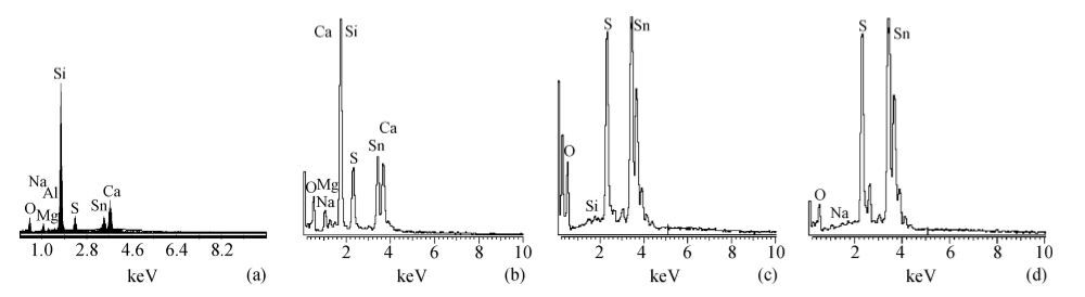
Fig. 1.
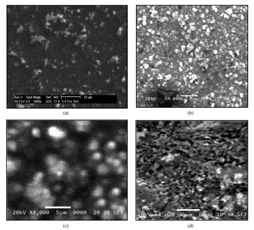
EDAX spectra of as-deposited SnS thin film samples (a) S1,(b) S2,(c) S3 and (d) S4.
SEMICONDUCTOR MATERIALS
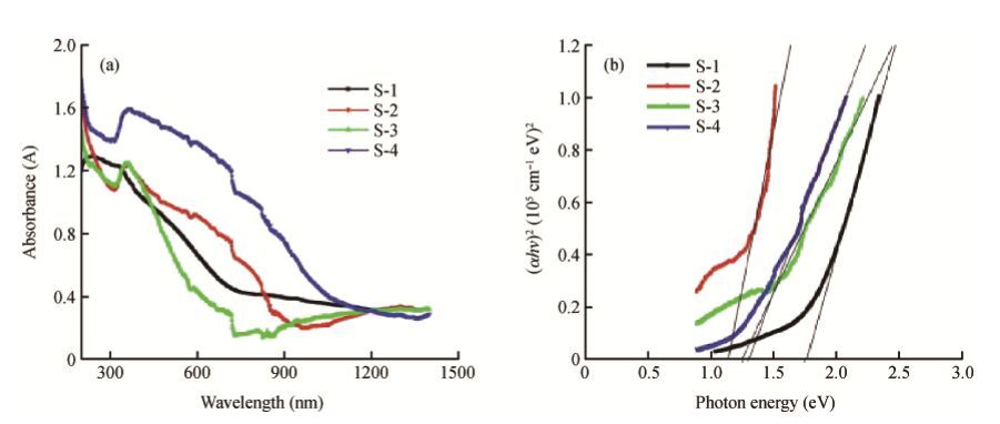
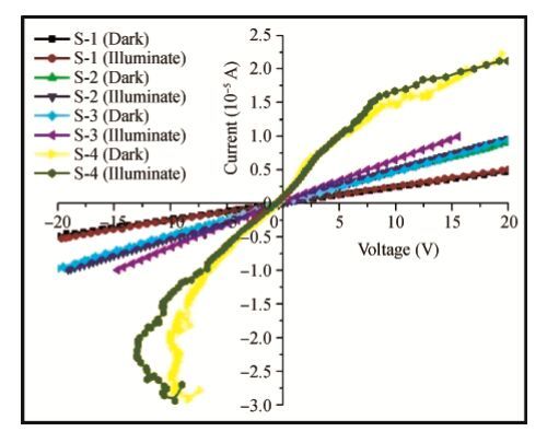
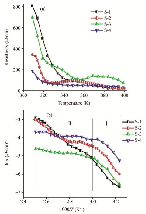
Abstract: The SnS thin films were synthesized by chemical bath deposition (CBD), dip coating and successive ionic layer adsorption and reaction (SILAR) techniques. In them, the CBD thin films were deposited at two temperatures: ambient and 70 ℃. The energy dispersive analysis of X-rays (EDAX), X-ray diffraction (XRD), Raman spectroscopy, scanning electron microscopy (SEM) and optical spectroscopy techniques were used to characterize the thin films. The electrical transport properties studies on the as-deposited thin films were done by measuring the I-V characteristics, DC electrical resistivity variation with temperature and the room temperature Hall effect. The obtained results are deliberated in this paper.
Key words: SnS, thin films, chemical bath deposition, dip coating, SILAR
| [1] | |
| [2] | |
| [3] | |
| [4] | |
| [5] | |
| [6] | |
| [7] | |
| [8] | |
| [9] | |
| [10] | |
| [11] | |
| [12] | |
| [13] | |
| [14] | |
| [15] | |
| [16] | |
| [17] | |
| [18] | |
| [19] | |
| [20] | |
| [21] | |
| [22] | |
| [23] | |
| [24] | |
| [25] | |
| [26] | |
| [27] | |
| [28] | |
| [29] | |
| [30] | |
| [31] | |
| [32] | |
| [33] | |
| [34] | |
| [35] | |
| [36] | |
| [37] | |
| [38] | |
| [39] | |
| [40] | |
| [41] |


Article views: 4057 Times PDF downloads: 88 Times Cited by: 0 Times
Received: 18 August 2015 Revised: Online: Published: 01 May 2016
| Citation: |
Sunil H. Chaki, Mahesh D. Chaudhary, M. P. Deshpande. SnS thin films deposited by chemical bath deposition, dip coating and SILAR techniques[J]. Journal of Semiconductors, 2016, 37(5): 053001. doi: 10.1088/1674-4926/37/5/053001
****
S. H. Chaki, M. D. Chaudhary, M. P. Deshpande. SnS thin films deposited by chemical bath deposition, dip coating and SILAR techniques[J]. J. Semicond., 2016, 37(5): 053001. doi: 10.1088/1674-4926/37/5/053001.

|
| [1] | |
| [2] | |
| [3] | |
| [4] | |
| [5] | |
| [6] | |
| [7] | |
| [8] | |
| [9] | |
| [10] | |
| [11] | |
| [12] | |
| [13] | |
| [14] | |
| [15] | |
| [16] | |
| [17] | |
| [18] | |
| [19] | |
| [20] | |
| [21] | |
| [22] | |
| [23] | |
| [24] | |
| [25] | |
| [26] | |
| [27] | |
| [28] | |
| [29] | |
| [30] | |
| [31] | |
| [32] | |
| [33] | |
| [34] | |
| [35] | |
| [36] | |
| [37] | |
| [38] | |
| [39] | |
| [40] | |
| [41] |

 WeChat ID
Journal of Semiconductors © 2017 All Rights Reserved 京ICP备05085259号-2

 DownLoad:

