J. Semicond. > 2022, Volume 43 > Issue 1 > 012301

ARTICLES

Investigation into the InAs/GaAs quantum dot material epitaxially grown on silicon for O band lasers

Tianyi Tang1, 2, 3, Tian Yu1, 2, 3, Guanqing Yang1, 2, 3, Jiaqian Sun1, 2, 3, Wenkang Zhan1, 2, 3, Bo Xu1, 2, 3, , Chao Zhao1, 2, 3, and Zhanguo Wang1, 2, 3

+ Author Affiliations

 Corresponding author: Bo Xu, srex@semi.ac.cn; Chao Zhao, zhaochao@semi.ac.cn

DOI: 10.1088/1674-4926/43/1/012301

PDF

Turn off MathJax

Abstract: InAs/GaAs quantum dot (QD) lasers were grown on silicon substrates using a thin Ge buffer and three-step growth method in the molecular beam epitaxy (MBE) system. In addition, strained superlattices were used to prevent threading dislocations from propagating to the active region of the laser. The as-grown material quality was characterized by the transmission electron microscope, scanning electron microscope, X-ray diffraction, atomic force microscope, and photoluminescence spectroscopy. The results show that a high-quality GaAs buffer with few dislocations was obtained by the growth scheme we developed. A broad-area edge-emitting laser was also fabricated. The O-band laser exhibited a threshold current density of 540 A/cm2 at room temperature under continuous wave conditions. This work demonstrates the potential of large-scale and low-cost manufacturing of the O-band InAs/GaAs quantum dot lasers on silicon substrates.

Key words: semiconductor lasermolecular beam epitaxyquantum dotsIII–V on Sisilicon photonics


[1]
Won R. Integrating silicon photonics. Nat Photonics, 2010, 4, 498 doi: 10.1038/nphoton.2010.189
[2]
Miller D. Device requirements for optical interconnects to silicon chips. Proc IEEE, 2009, 97, 1166 doi: 10.1109/JPROC.2009.2014298
[3]
Zhou Z, Chen R, Li X, et al. Development trends in silicon photonics for data centers. Opt Fiber Technol, 2018, 44, 13 doi: 10.1016/j.yofte.2018.03.009
[4]
Rickman A. The commercialization of silicon photonics. Nat Photonics, 2014, 8, 579 doi: 10.1038/nphoton.2014.175
[5]
Liang D, Bowers J E. Recent progress in lasers on silicon. Nat Photonics, 2010, 4, 511 doi: 10.1038/nphoton.2010.167
[6]
Wirths S, Geiger R, von den Driesch N, et al. Lasing in direct-bandgap GeSn alloy grown on Si. Nat Photonics, 2015, 9, 88 doi: 10.1038/nphoton.2014.321
[7]
Tang M, Park J S, Wang Z, et al. Integration of III–V lasers on Si for Si photonics. Prog Quantum Electron, 2019, 66, 1 doi: 10.1016/j.pquantelec.2019.05.002
[8]
Wang J, Ren X, Deng C, et al. Extremely low-threshold current density InGaAs/AlGaAs quantum-well lasers on silicon. J Lightwave Technol, 2015, 33, 3163 doi: 10.1109/JLT.2015.2438873
[9]
Rio Calvo M, Monge Bartolomé L, Bahriz M, et al. Mid-infrared laser diodes epitaxially grown on on-axis (001) silicon. Optica, 2020, 7, 263 doi: 10.1364/OPTICA.388383
[10]
Wang Z, Van Gasse K, Moskalenko V, et al. A III–V-on-Si ultra-dense comb laser. Light Sci Appl, 2017, 6, e16260 doi: 10.1038/lsa.2016.260
[11]
Billah M R, Blaicher M, Hoose T, et al. Hybrid integration of silicon photonics circuits and InP lasers by photonic wire bonding. Optica, 2018, 5, 876 doi: 10.1364/OPTICA.5.000876
[12]
Jang B, Tanabe K, Kako S, et al. A hybrid silicon evanescent quantum dot laser. Appl Phys Express, 2016, 9, 092102 doi: 10.7567/APEX.9.092102
[13]
Jhang Y H, Mochida R, Tanabe K, et al. Direct modulation of 1.3 μm quantum dot lasers on silicon at 60 °C. Opt Express, 2016, 24, 18428 doi: 10.1109/ICIPRM.2016.7528534
[14]
Chen S, Li W, Wu J, et al. Electrically pumped continuous-wave III–V quantum dot lasers on silicon. Nat Photonics, 2016, 10, 307 doi: 10.1038/nphoton.2016.21
[15]
Liao M, Chen S, Park J S, et al. III–V quantum-dot lasers monolithically grown on silicon. Semicond Sci Technol, 2018, 33, 123002 doi: 10.1088/1361-6641/aae6a5
[16]
Park J S, Tang M, Chen S, et al. Heteroepitaxial growth of III–V semiconductors on silicon. Crystals, 2020, 10, 1163 doi: 10.3390/cryst10121163
[17]
Matthews J W, Blakeslee A E. Defects in epitaxial multilayers. J Cryst Growth, 1974, 27, 118 doi: 10.1016/S0022-0248(74)80055-2
[18]
Li Q, Lau K M. Epitaxial growth of highly mismatched III–V materials on (001) silicon for electronics and optoelectronics. Prog Cryst Growth Charact Mater, 2017, 63, 105 doi: 10.1016/j.pcrysgrow.2017.10.001
[19]
Georgakilas A, Stoemenos J, Tsagaraki K, et al. Generation and annihilation of antiphase domain boundaries in GaAs on Si grown by molecular beam epitaxy. J Mater Res, 1993, 8, 1908 doi: 10.1557/JMR.1993.1908
[20]
Kroemer H. Polar-on-nonpolar epitaxy. J Cryst Growth, 1987, 81, 193 doi: 10.1016/0022-0248(87)90391-5
[21]
Ye T, Suo Z, Evans A G. Thin film cracking and the roles of substrate and interface. Int J Solids Struct, 1992, 29, 2639 doi: 10.1016/0020-7683(92)90227-K
[22]
Wei W, Feng Q, Wang Z, et al. Perspective: optically-pumped III–V quantum dot microcavity lasers via CMOS compatible patterned Si (001) substrates. J Semicond, 2019, 40, 101303 doi: 10.1088/1674-4926/40/10/101303
[23]
Ward T, Sánchez A M, Tang M, et al. Design rules for dislocation filters. J Appl Phys, 2014, 116, 063508 doi: 10.1063/1.4892162
[24]
Beanland R, Sánchez A M, Childs D, et al. Structural analysis of life tested 1.3 μm quantum dot lasers. J Appl Phys, 2008, 103, 014913 doi: 10.1063/1.2827451
[25]
Arakawa Y, Sakaki H. Multidimensional quantum well laser and temperature dependence of its threshold current. Appl Phys Lett, 1982, 40, 939 doi: 10.1063/1.92959
[26]
Jung D, Callahan P G, Shin B, et al. Low threading dislocation density GaAs growth on on-axis GaP/Si (001). J Appl Phys, 2017, 122, 225703 doi: 10.1063/1.5001360
[27]
Lee A, Jiang Q, Tang M, et al. Continuous-wave InAs/GaAs quantum-dot laser diodes monolithically grown on Si substrate with low threshold current densities. Opt Express, 2012, 20, 22181 doi: 10.1364/OE.20.022181
[28]
Li K, Yang J, Lu Y, et al. Inversion boundary annihilation in GaAs monolithically grown on on-axis silicon (001). Adv Opt Mater, 2020, 8, 2000970 doi: 10.1002/adom.202000970
[29]
Kwoen J, Jang B, Lee J, et al. All MBE grown InAs/GaAs quantum dot lasers on on-axis Si (001). Opt Express, 2018, 26, 11568 doi: 10.1364/OE.26.011568
[30]
Wei W Q, Wang J H, Zhang B, et al. InAs QDs on (111)-faceted Si (001) hollow substrates with strong emission at 1300 nm and 1550 nm. Appl Phys Lett, 2018, 113, 053107 doi: 10.1063/1.5043169
[31]
Li Q, Ng K W, Lau K M. Growing antiphase-domain-free GaAs thin films out of highly ordered planar nanowire arrays on exact (001) silicon. Appl Phys Lett, 2015, 106, 072105 doi: 10.1063/1.4913432
[32]
Shi B, Wang L, Taylor A A, et al. MOCVD grown low dislocation density GaAs-on-V-groove patterned (001) Si for 1.3 μm quantum dot laser applications. Appl Phys Lett, 2019, 114, 172102 doi: 10.1063/1.5090437
[33]
Hayafuji N, Kizuki H, Miyashita M, et al. Crack propagation and mechanical fracture in GaAs-on-Si. Jpn J Appl Phys, 1991, 30, 459 doi: 10.1143/JJAP.30.459
[34]
Sieg R M, Ringel S A, Ting S M, et al. Anti-phase domain-free growth of GaAs on offcut (001) Ge wafers by molecular beam epitaxy with suppressed Ge outdiffusion. J Electron Mater, 1998, 27, 900 doi: 10.1007/s11664-998-0116-1
[35]
Choi D, Harris J S, Kim E, et al. High-quality III–V semiconductor MBE growth on Ge/Si virtual substrates for metal-oxide-semiconductor device fabrication. J Cryst Growth, 2009, 311, 1962 doi: 10.1016/j.jcrysgro.2008.09.138
[36]
Yamaguchi M, Tachikawa M, Itoh Y, et al. Thermal annealing effects of defect reduction in GaAs on Si substrates. J Appl Phys, 1990, 68, 4518 doi: 10.1063/1.346156
[37]
Guo D, Jiang Q, Tang M, et al. Two-colour In0.5Ga0.5As quantum dot infrared photodetectors on silicon. Semicond Sci Technol, 2018, 33, 094009 doi: 10.1088/1361-6641/aad83c
[38]
Gao F, Wen L, Guan Y, et al. Strain relaxation of the In0.53Ga0.47As epi-layer grown on a Si substrate using molecular beam epitaxy. CrystEngComm, 2014, 16, 10721 doi: 10.1039/C4CE01607F
[39]
Hudait M K, Clavel M, Goley P, et al. Heterogeneous integration of epitaxial Ge on Si using AlAs/GaAs buffer architecture: suitability for low-power fin field-effect transistors. Sci Rep, 2014, 4, 6964 doi: 10.1038/srep06964
[40]
Du Y, Kong Z, Toprak M S, et al. Investigation of the heteroepitaxial process optimization of Ge layers on Si (001) by RPCVD. Nanomaterials, 2021, 11, 928 doi: 10.3390/nano11040928
[41]
Du Y, Xu B, Wang G, et al. Growth of high-quality epitaxy of GaAs on Si with engineered Ge buffer using MOCVD. J Mater Sci: Mater Electron, 2021, 32, 6425 doi: 10.1007/s10854-021-05360-4
[42]
Eisele H, Lenz A, Heitz R, et al. Change of InAs/GaAs quantum dot shape and composition during capping. J Appl Phys, 2008, 104, 124301 doi: 10.1063/1.3042216
[43]
Chen R, Liu H Y, Sun H D. Electronic energy levels and carrier dynamics in InAs/InGaAs dots-in-a-well structure investigated by optical spectroscopy. J Appl Phys, 2010, 107, 013513 doi: 10.1063/1.3277049
[44]
Tarasov G G, Mazur Y I, Zhuchenko Z Y, et al. Carrier transfer in self-assembled coupled InAs/GaAs quantum dots. J Appl Phys, 2000, 88, 7162 doi: 10.1063/1.1323516
[45]
Popescu D P, Eliseev P G, Stintz A, et al. Temperature dependence of the photoluminescence emission from InAs quantum dots in a strained Ga0.85In0.15As quantum well. Semicond Sci Technol, 2004, 19, 33 doi: 10.1088/0268-1242/19/1/005
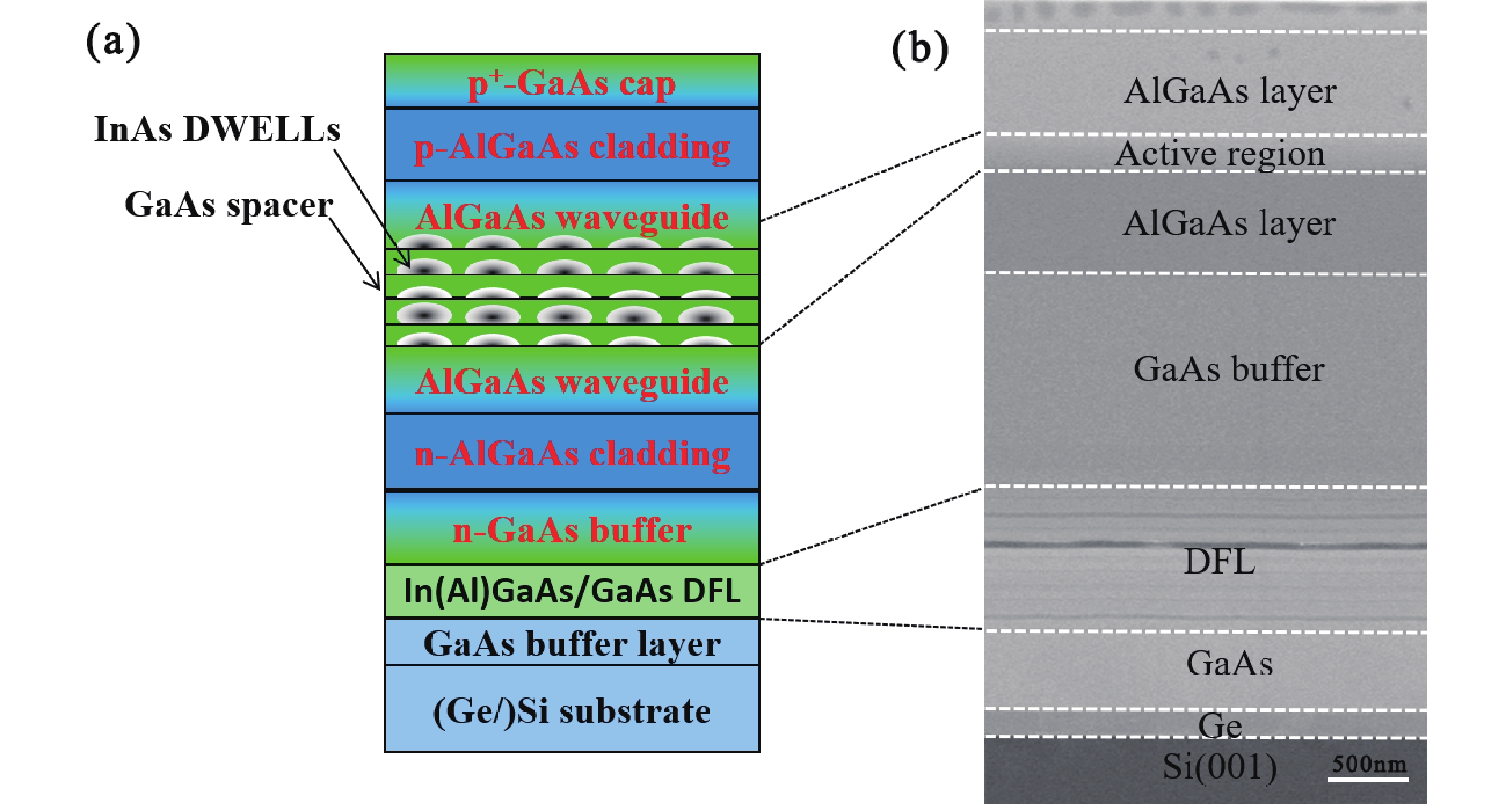
Fig. 1.  (Color online) (a) Schematic of the QD laser structure grown on silicon substrates, and (b) the corresponding cross-sectional SEM image.

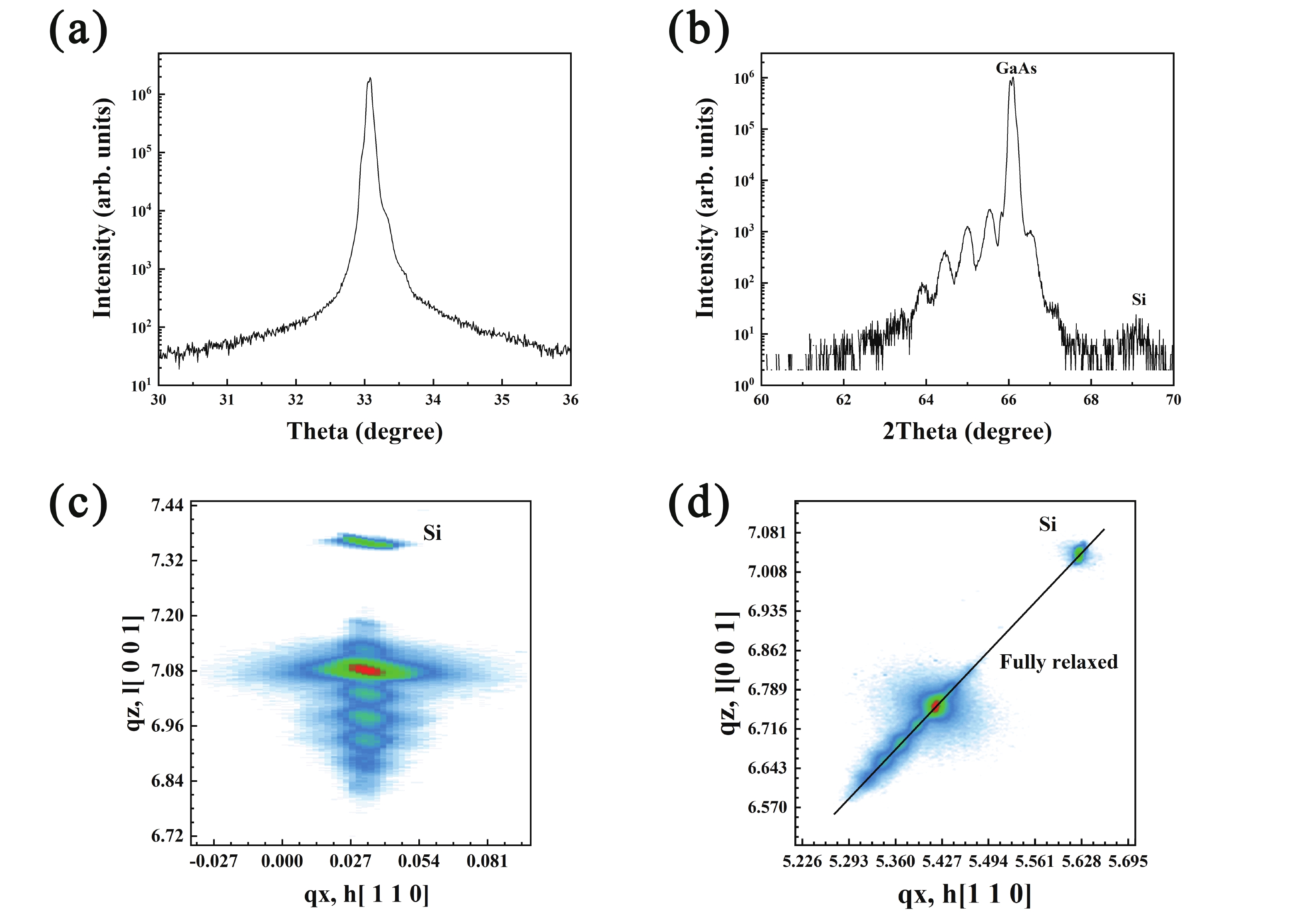
Fig. 2.  (Color online) (a) XRD RC around GaAs (004). (b) High resolution XRD (004) scan of GaAs grown on Si. High resolution XRD RSM results taken from (c) (004) and (d) (224) reflections.

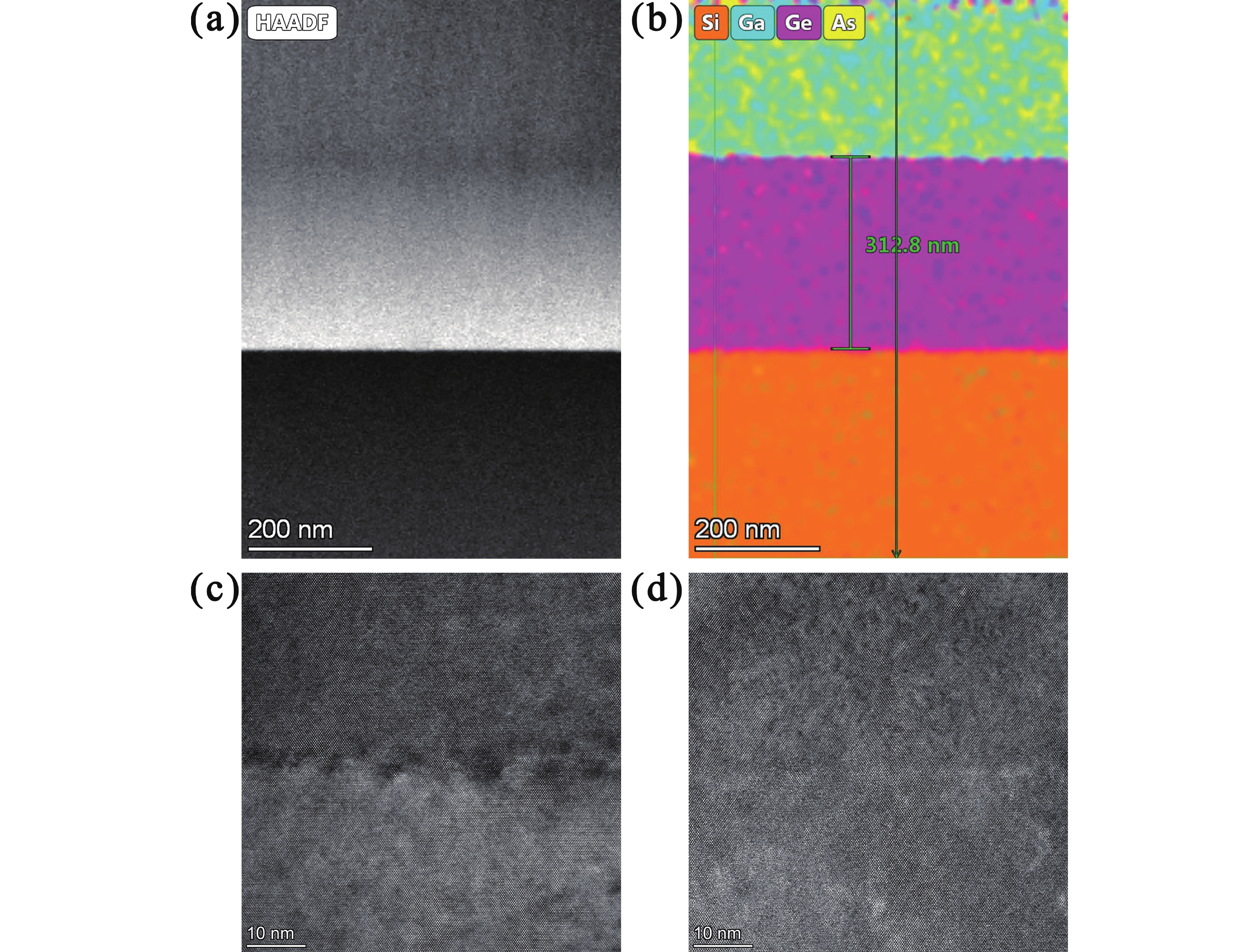
Fig. 3.  (Color online) (a) Cross-sectional TEM high-angle annular dark field image (HAADF) of GaAs grown on the Ge/Si virtual substrate. (b) Elemental mapping of the interface between GaAs layer, Ge layer and Si substrate. High resolution cross-sectional TEM image of the interface between (c) Ge layer and Si, and (d) GaAs layer and Ge layer, respectively.

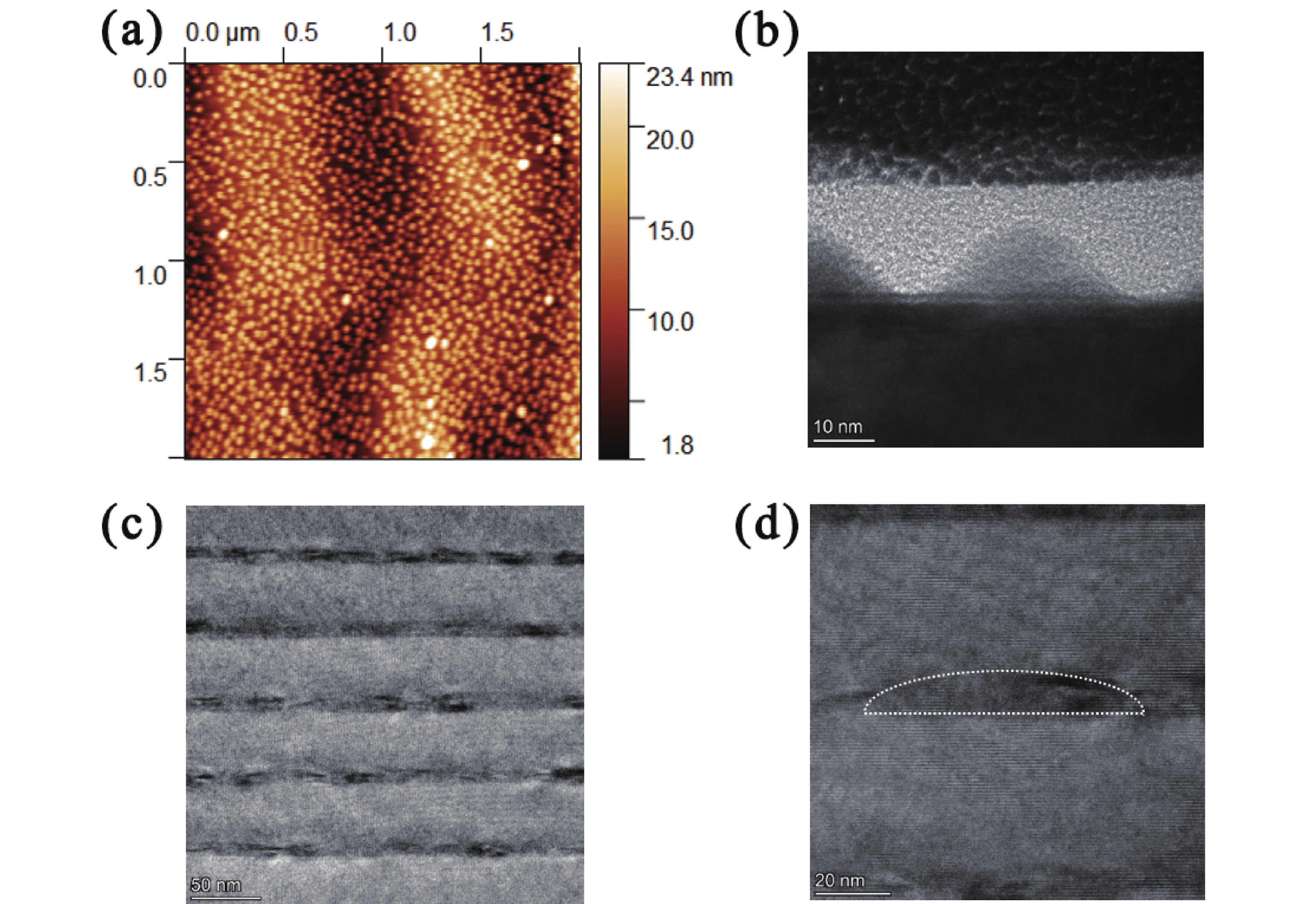
Fig. 4.  (Color online) (a) A 2 × 2 μm2 AFM image of surface InAs QDs grown on Si substrates. (b) Cross-sectional TEM images of surface InAs QDs on Si substrates. (c) Cross-sectional TEM images of the active region of the laser grown on Si substrates. (d) High-resolution TEM images of InAs QDs in the active region.

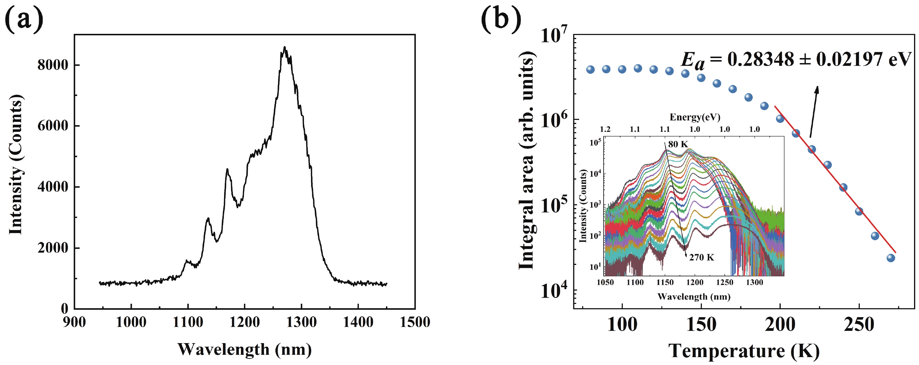
Fig. 5.  (Color online) (a) PL spectrum of InAs DWELL grown on Si substrates. (b) Temperature-dependences of the integrated PL intensity. Inset: temperature-dependent PL spectra of the InAs QD grown on Si substrates.

Fig. 6.  (Color online) (a) L–I–V curve of InAs QD lasers grown on Si substrates under pulsed mode at room temperature. Inset: SEM image of the whole InAs QD laser structure on the Si substrate. (b) L–I curve of InAs QD lasers grown on Si substrates under CW mode. (c) Emission spectrum of InAs QD laser grown on Si substrates under RT and CW modes.

[1]
Won R. Integrating silicon photonics. Nat Photonics, 2010, 4, 498 doi: 10.1038/nphoton.2010.189
[2]
Miller D. Device requirements for optical interconnects to silicon chips. Proc IEEE, 2009, 97, 1166 doi: 10.1109/JPROC.2009.2014298
[3]
Zhou Z, Chen R, Li X, et al. Development trends in silicon photonics for data centers. Opt Fiber Technol, 2018, 44, 13 doi: 10.1016/j.yofte.2018.03.009
[4]
Rickman A. The commercialization of silicon photonics. Nat Photonics, 2014, 8, 579 doi: 10.1038/nphoton.2014.175
[5]
Liang D, Bowers J E. Recent progress in lasers on silicon. Nat Photonics, 2010, 4, 511 doi: 10.1038/nphoton.2010.167
[6]
Wirths S, Geiger R, von den Driesch N, et al. Lasing in direct-bandgap GeSn alloy grown on Si. Nat Photonics, 2015, 9, 88 doi: 10.1038/nphoton.2014.321
[7]
Tang M, Park J S, Wang Z, et al. Integration of III–V lasers on Si for Si photonics. Prog Quantum Electron, 2019, 66, 1 doi: 10.1016/j.pquantelec.2019.05.002
[8]
Wang J, Ren X, Deng C, et al. Extremely low-threshold current density InGaAs/AlGaAs quantum-well lasers on silicon. J Lightwave Technol, 2015, 33, 3163 doi: 10.1109/JLT.2015.2438873
[9]
Rio Calvo M, Monge Bartolomé L, Bahriz M, et al. Mid-infrared laser diodes epitaxially grown on on-axis (001) silicon. Optica, 2020, 7, 263 doi: 10.1364/OPTICA.388383
[10]
Wang Z, Van Gasse K, Moskalenko V, et al. A III–V-on-Si ultra-dense comb laser. Light Sci Appl, 2017, 6, e16260 doi: 10.1038/lsa.2016.260
[11]
Billah M R, Blaicher M, Hoose T, et al. Hybrid integration of silicon photonics circuits and InP lasers by photonic wire bonding. Optica, 2018, 5, 876 doi: 10.1364/OPTICA.5.000876
[12]
Jang B, Tanabe K, Kako S, et al. A hybrid silicon evanescent quantum dot laser. Appl Phys Express, 2016, 9, 092102 doi: 10.7567/APEX.9.092102
[13]
Jhang Y H, Mochida R, Tanabe K, et al. Direct modulation of 1.3 μm quantum dot lasers on silicon at 60 °C. Opt Express, 2016, 24, 18428 doi: 10.1109/ICIPRM.2016.7528534
[14]
Chen S, Li W, Wu J, et al. Electrically pumped continuous-wave III–V quantum dot lasers on silicon. Nat Photonics, 2016, 10, 307 doi: 10.1038/nphoton.2016.21
[15]
Liao M, Chen S, Park J S, et al. III–V quantum-dot lasers monolithically grown on silicon. Semicond Sci Technol, 2018, 33, 123002 doi: 10.1088/1361-6641/aae6a5
[16]
Park J S, Tang M, Chen S, et al. Heteroepitaxial growth of III–V semiconductors on silicon. Crystals, 2020, 10, 1163 doi: 10.3390/cryst10121163
[17]
Matthews J W, Blakeslee A E. Defects in epitaxial multilayers. J Cryst Growth, 1974, 27, 118 doi: 10.1016/S0022-0248(74)80055-2
[18]
Li Q, Lau K M. Epitaxial growth of highly mismatched III–V materials on (001) silicon for electronics and optoelectronics. Prog Cryst Growth Charact Mater, 2017, 63, 105 doi: 10.1016/j.pcrysgrow.2017.10.001
[19]
Georgakilas A, Stoemenos J, Tsagaraki K, et al. Generation and annihilation of antiphase domain boundaries in GaAs on Si grown by molecular beam epitaxy. J Mater Res, 1993, 8, 1908 doi: 10.1557/JMR.1993.1908
[20]
Kroemer H. Polar-on-nonpolar epitaxy. J Cryst Growth, 1987, 81, 193 doi: 10.1016/0022-0248(87)90391-5
[21]
Ye T, Suo Z, Evans A G. Thin film cracking and the roles of substrate and interface. Int J Solids Struct, 1992, 29, 2639 doi: 10.1016/0020-7683(92)90227-K
[22]
Wei W, Feng Q, Wang Z, et al. Perspective: optically-pumped III–V quantum dot microcavity lasers via CMOS compatible patterned Si (001) substrates. J Semicond, 2019, 40, 101303 doi: 10.1088/1674-4926/40/10/101303
[23]
Ward T, Sánchez A M, Tang M, et al. Design rules for dislocation filters. J Appl Phys, 2014, 116, 063508 doi: 10.1063/1.4892162
[24]
Beanland R, Sánchez A M, Childs D, et al. Structural analysis of life tested 1.3 μm quantum dot lasers. J Appl Phys, 2008, 103, 014913 doi: 10.1063/1.2827451
[25]
Arakawa Y, Sakaki H. Multidimensional quantum well laser and temperature dependence of its threshold current. Appl Phys Lett, 1982, 40, 939 doi: 10.1063/1.92959
[26]
Jung D, Callahan P G, Shin B, et al. Low threading dislocation density GaAs growth on on-axis GaP/Si (001). J Appl Phys, 2017, 122, 225703 doi: 10.1063/1.5001360
[27]
Lee A, Jiang Q, Tang M, et al. Continuous-wave InAs/GaAs quantum-dot laser diodes monolithically grown on Si substrate with low threshold current densities. Opt Express, 2012, 20, 22181 doi: 10.1364/OE.20.022181
[28]
Li K, Yang J, Lu Y, et al. Inversion boundary annihilation in GaAs monolithically grown on on-axis silicon (001). Adv Opt Mater, 2020, 8, 2000970 doi: 10.1002/adom.202000970
[29]
Kwoen J, Jang B, Lee J, et al. All MBE grown InAs/GaAs quantum dot lasers on on-axis Si (001). Opt Express, 2018, 26, 11568 doi: 10.1364/OE.26.011568
[30]
Wei W Q, Wang J H, Zhang B, et al. InAs QDs on (111)-faceted Si (001) hollow substrates with strong emission at 1300 nm and 1550 nm. Appl Phys Lett, 2018, 113, 053107 doi: 10.1063/1.5043169
[31]
Li Q, Ng K W, Lau K M. Growing antiphase-domain-free GaAs thin films out of highly ordered planar nanowire arrays on exact (001) silicon. Appl Phys Lett, 2015, 106, 072105 doi: 10.1063/1.4913432
[32]
Shi B, Wang L, Taylor A A, et al. MOCVD grown low dislocation density GaAs-on-V-groove patterned (001) Si for 1.3 μm quantum dot laser applications. Appl Phys Lett, 2019, 114, 172102 doi: 10.1063/1.5090437
[33]
Hayafuji N, Kizuki H, Miyashita M, et al. Crack propagation and mechanical fracture in GaAs-on-Si. Jpn J Appl Phys, 1991, 30, 459 doi: 10.1143/JJAP.30.459
[34]
Sieg R M, Ringel S A, Ting S M, et al. Anti-phase domain-free growth of GaAs on offcut (001) Ge wafers by molecular beam epitaxy with suppressed Ge outdiffusion. J Electron Mater, 1998, 27, 900 doi: 10.1007/s11664-998-0116-1
[35]
Choi D, Harris J S, Kim E, et al. High-quality III–V semiconductor MBE growth on Ge/Si virtual substrates for metal-oxide-semiconductor device fabrication. J Cryst Growth, 2009, 311, 1962 doi: 10.1016/j.jcrysgro.2008.09.138
[36]
Yamaguchi M, Tachikawa M, Itoh Y, et al. Thermal annealing effects of defect reduction in GaAs on Si substrates. J Appl Phys, 1990, 68, 4518 doi: 10.1063/1.346156
[37]
Guo D, Jiang Q, Tang M, et al. Two-colour In0.5Ga0.5As quantum dot infrared photodetectors on silicon. Semicond Sci Technol, 2018, 33, 094009 doi: 10.1088/1361-6641/aad83c
[38]
Gao F, Wen L, Guan Y, et al. Strain relaxation of the In0.53Ga0.47As epi-layer grown on a Si substrate using molecular beam epitaxy. CrystEngComm, 2014, 16, 10721 doi: 10.1039/C4CE01607F
[39]
Hudait M K, Clavel M, Goley P, et al. Heterogeneous integration of epitaxial Ge on Si using AlAs/GaAs buffer architecture: suitability for low-power fin field-effect transistors. Sci Rep, 2014, 4, 6964 doi: 10.1038/srep06964
[40]
Du Y, Kong Z, Toprak M S, et al. Investigation of the heteroepitaxial process optimization of Ge layers on Si (001) by RPCVD. Nanomaterials, 2021, 11, 928 doi: 10.3390/nano11040928
[41]
Du Y, Xu B, Wang G, et al. Growth of high-quality epitaxy of GaAs on Si with engineered Ge buffer using MOCVD. J Mater Sci: Mater Electron, 2021, 32, 6425 doi: 10.1007/s10854-021-05360-4
[42]
Eisele H, Lenz A, Heitz R, et al. Change of InAs/GaAs quantum dot shape and composition during capping. J Appl Phys, 2008, 104, 124301 doi: 10.1063/1.3042216
[43]
Chen R, Liu H Y, Sun H D. Electronic energy levels and carrier dynamics in InAs/InGaAs dots-in-a-well structure investigated by optical spectroscopy. J Appl Phys, 2010, 107, 013513 doi: 10.1063/1.3277049
[44]
Tarasov G G, Mazur Y I, Zhuchenko Z Y, et al. Carrier transfer in self-assembled coupled InAs/GaAs quantum dots. J Appl Phys, 2000, 88, 7162 doi: 10.1063/1.1323516
[45]
Popescu D P, Eliseev P G, Stintz A, et al. Temperature dependence of the photoluminescence emission from InAs quantum dots in a strained Ga0.85In0.15As quantum well. Semicond Sci Technol, 2004, 19, 33 doi: 10.1088/0268-1242/19/1/005
1

Avalanche photodiodes on silicon photonics

Yuan Yuan, Bassem Tossoun, Zhihong Huang, Xiaoge Zeng, Geza Kurczveil, et al.

Journal of Semiconductors, 2022, 43(2): 021301. doi: 10.1088/1674-4926/43/2/021301

2

Perspective: optically-pumped III–V quantum dot microcavity lasers via CMOS compatible patterned Si (001) substrates

Wenqi Wei, Qi Feng, Zihao Wang, Ting Wang, Jianjun Zhang, et al.

Journal of Semiconductors, 2019, 40(10): 101303. doi: 10.1088/1674-4926/40/10/101303

3

Recent progress in epitaxial growth of III–V quantum-dot lasers on silicon substrate

Shujie Pan, Victoria Cao, Mengya Liao, Ying Lu, Zizhuo Liu, et al.

Journal of Semiconductors, 2019, 40(10): 101302. doi: 10.1088/1674-4926/40/10/101302

4

Quantum light source devices of In(Ga)As semiconductor self-assembled quantum dots

Xiaowu He, Yifeng Song, Ying Yu, Ben Ma, Zesheng Chen, et al.

Journal of Semiconductors, 2019, 40(7): 071902. doi: 10.1088/1674-4926/40/7/071902

5

Controllable growth of GeSi nanostructures by molecular beam epitaxy

Yingjie Ma, Tong Zhou, Zhenyang Zhong, Zuimin Jiang

Journal of Semiconductors, 2018, 39(6): 061004. doi: 10.1088/1674-4926/39/6/061004

6

Review of recent progresses on flexible oxide semiconductor thin film transistors based on atomic layer deposition processes

Jiazhen Sheng, Ki-Lim Han, TaeHyun Hong, Wan-Ho Choi, Jin-Seong Park, et al.

Journal of Semiconductors, 2018, 39(1): 011008. doi: 10.1088/1674-4926/39/1/011008

7

The developing condition analysis of semiconductor laser frequency stabilization technology

Yijun Yao, Canwen Zou, Haiyang Yu, Jinjin Guo, Yaming Li, et al.

Journal of Semiconductors, 2018, 39(11): 114004. doi: 10.1088/1674-4926/39/11/114004

8

Researching the 915 nm high-power and high-brightness semiconductor laser single chip coupling module

Xin Wang, Cuiluan Wang, Xia Wu, Lingni Zhu, Hongqi Jing, et al.

Journal of Semiconductors, 2017, 38(2): 024006. doi: 10.1088/1674-4926/38/2/024006

9

Progress in complementary metal-oxide-semiconductor silicon photonics and optoelectronic integrated circuits

Hongda Chen, Zan Zhang, Beiju Huang, Luhong Mao, Zanyun Zhang, et al.

Journal of Semiconductors, 2015, 36(12): 121001. doi: 10.1088/1674-4926/36/12/121001

10

Large-signal characterizations of DDR IMPATT devices based on group Ⅲ-Ⅴ semiconductors at millimeter-wave and terahertz frequencies

Aritra Acharyya, Aliva Mallik, Debopriya Banerjee, Suman Ganguli, Arindam Das, et al.

Journal of Semiconductors, 2014, 35(8): 084003. doi: 10.1088/1674-4926/35/8/084003

11

Influence of doping position on the extinction ratio of Mach-Zehnder-interference based silicon optical modulators

Zhao Yong, Wang Wanjun, Shao Haifeng, Yang Jianyi, Wang Minghua, et al.

Journal of Semiconductors, 2012, 33(1): 014009. doi: 10.1088/1674-4926/33/1/014009

12

A theoretical model of the femtosecond laser ablation of semiconductors considering inverse bremsstrahlung absorption

Lin Xiaohui, Zhang Chibin, Ren Weisong, Jiang Shuyun, Ouyang Quanhui, et al.

Journal of Semiconductors, 2012, 33(4): 046002. doi: 10.1088/1674-4926/33/4/046002

13

Thermal analysis of the cavity facet for an 808 nm semiconductor laser by using near-field scanning optical microscopy

Rao Lan, Song Guofeng, Chen Lianghui

Journal of Semiconductors, 2010, 31(10): 104007. doi: 10.1088/1674-4926/31/10/104007

14

Terahertz Semiconductor Quantum Well Devices

Liu H C, Luo H, Ban D, Wachter M, Song C Y, et al.

Chinese Journal of Semiconductors , 2006, 27(4): 627-634.

15

Low Voltage Flash Memory Cells Using SiGe Quantum Dots for Enhancing F-N Tunneling

Deng Ning, Pan Liyang, Liu Zhihong, Zhu Jun, Chen Peiyi, et al.

Chinese Journal of Semiconductors , 2006, 27(3): 454-458.

16

Temperature Dependence of Vacuum Rabi Splitting in a Single Quantum Dot-Semiconductor Microcavity

Zhu Kadi, Li Waisang

Chinese Journal of Semiconductors , 2006, 27(3): 489-493.

17

1.3μm InGaAs/InAs/GaAs Self-Assembled Quantum Dot Laser Diode Grown by Molecular Beam Epitaxy

Niu Zhichuan, Ni Haiqiao, Fang Zhidan, Gong Zheng, Zhang Shiyong, et al.

Chinese Journal of Semiconductors , 2006, 27(3): 482-488.

18

Material Growth and Device Fabrication of GaAs Based 1.3μm GaInNAs Quantum Well Laser Diodes

Chinese Journal of Semiconductors , 2005, 26(9): 1860-1864.

19

Passively Mode Locked Diode-End-Pumped Yb∶YAB Laser with High Reflectivity Type Semiconductor Saturable Absorption Mirror

Wang Yonggang, Ma Xiaoyu, Xue Yinghong, Sun Hong,Zhang Zhigang,and Wang Qingyue

Chinese Journal of Semiconductors , 2005, 26(2): 250-253.

20

Growth of Space Ordered 1.3μm InAs Quantum Dots on GaAs(100) Vicinal Substrates by MOCVD

Liang Song, Zhu Hongliang, Pan Jiaoqing, Wang Wei

Chinese Journal of Semiconductors , 2005, 26(11): 2074-2079.

1. Ye, J., Liu, H., Jiang, C. et al. Antiphase-Boundary-Free GaAs Grown via MBE on an On-Axis Si(001) Substrate with High-Temperature Surface Step Pretreatment. Crystal Growth and Design, 2025. doi:10.1021/acs.cgd.4c01384
2. Li, X., Shah, A.A., Abbas, M. et al. Suppression of Deep-Level Defects and Interface Modification in Antimony Sulfide Thin-Film Solar Cells Via Solution-Processed Sulfurization. ACS Applied Energy Materials, 2024, 7(14): 5848-5856. doi:10.1021/acsaem.4c01013
3. Laryn, T., Chu, R.J., Kim, Y. et al. Reduction of GaAs Buffer Thickness and Its Impact on Epitaxially Integrated III-V Quantum Dot Lasers on a Si Substrate. ACS Applied Materials and Interfaces, 2024, 16(23): 30209-30217. doi:10.1021/acsami.4c04597
4. Xie, C., Li, Y., Xu, C. et al. Epitaxial growth of high-quality Ge layers on Si with Ge2H6 under UHV-CVD conditions. Semiconductor Science and Technology, 2024, 39(1): 015008. doi:10.1088/1361-6641/ad14ee
5. Seravalli, L.. Metamorphic InAs/InGaAs quantum dots for optoelectronic devices: A review. Microelectronic Engineering, 2023. doi:10.1016/j.mee.2023.111996
6. Wang, Y., Ma, B., Li, J. et al. InAs/GaAs quantum-dot lasers grown on on-axis Si (001) without dislocation filter layers. Optics Express, 2023, 31(3): 4862-4872. doi:10.1364/OE.475976
7. Tang, T., Zhan, W., Shen, C. et al. High-quality GaSb epitaxially grown on Si (001) through defects self-annihilation for CMOS-compatible near-IR light emitters. Optical Materials Express, 2023, 13(1): 104-118. doi:10.1364/OME.474007
8. Abramkin, D.S., Atuchin, V.V. Novel InGaSb/AlP Quantum Dots for Non-Volatile Memories. Nanomaterials, 2022, 12(21): 3794. doi:10.3390/nano12213794
  • Search

    Advanced Search >>

    GET CITATION

    Tianyi Tang, Tian Yu, Guanqing Yang, Jiaqian Sun, Wenkang Zhan, Bo Xu, Chao Zhao, Zhanguo Wang. Investigation into the InAs/GaAs quantum dot material epitaxially grown on silicon for O band lasers[J]. Journal of Semiconductors, 2022, 43(1): 012301. doi: 10.1088/1674-4926/43/1/012301
    T Y Tang, T Yu, G Q Yang, J Q Sun, W K Zhan, B Xu, C Zhao, Z G Wang, Investigation into the InAs/GaAs quantum dot material epitaxially grown on silicon for O band lasers[J]. J. Semicond., 2022, 43(1): 012301. doi: 10.1088/1674-4926/43/1/012301.
    shu

    Export: BibTex EndNote

    Article Metrics

    Article views: 2811 Times PDF downloads: 145 Times Cited by: 8 Times

    History

    Received: 12 June 2021 Revised: 02 August 2021 Online: Accepted Manuscript: 29 September 2021Uncorrected proof: 29 September 2021Published: 04 January 2022

    Catalog

      Email This Article

      User name:
      Email:*请输入正确邮箱
      Code:*验证码错误
      Tianyi Tang, Tian Yu, Guanqing Yang, Jiaqian Sun, Wenkang Zhan, Bo Xu, Chao Zhao, Zhanguo Wang. Investigation into the InAs/GaAs quantum dot material epitaxially grown on silicon for O band lasers[J]. Journal of Semiconductors, 2022, 43(1): 012301. doi: 10.1088/1674-4926/43/1/012301 ****T Y Tang, T Yu, G Q Yang, J Q Sun, W K Zhan, B Xu, C Zhao, Z G Wang, Investigation into the InAs/GaAs quantum dot material epitaxially grown on silicon for O band lasers[J]. J. Semicond., 2022, 43(1): 012301. doi: 10.1088/1674-4926/43/1/012301.
      Citation:
      Tianyi Tang, Tian Yu, Guanqing Yang, Jiaqian Sun, Wenkang Zhan, Bo Xu, Chao Zhao, Zhanguo Wang. Investigation into the InAs/GaAs quantum dot material epitaxially grown on silicon for O band lasers[J]. Journal of Semiconductors, 2022, 43(1): 012301. doi: 10.1088/1674-4926/43/1/012301 ****
      T Y Tang, T Yu, G Q Yang, J Q Sun, W K Zhan, B Xu, C Zhao, Z G Wang, Investigation into the InAs/GaAs quantum dot material epitaxially grown on silicon for O band lasers[J]. J. Semicond., 2022, 43(1): 012301. doi: 10.1088/1674-4926/43/1/012301.

      Investigation into the InAs/GaAs quantum dot material epitaxially grown on silicon for O band lasers

      DOI: 10.1088/1674-4926/43/1/012301
      More Information
      • Tianyi Tang:received his B.Eng degree in Inorganic Non-Metallic Materials Engineering from Chang’an University, Xi’an, China, in 2017. He is currently studying as a doctoral student in Institute of Semiconductors, Chinese Academy of Sciences. His major is semiconductor materials and devices and research interests focus on silicon-based InAs/GaAs quantum dot lasers
      • Bo Xu:is a full professor in Institute of Semiconductors, Chinese Academy of Sciences. He is an expert on the growth of III–V compound semiconductor materials and optoelectronic devices by molecular beam epitaxy
      • Chao Zhao:is a full professor in Institute of Semiconductors, Chinese Academy of Sciences. He has a long and distinguished record of achievements in the fields of III–V compound semiconductor materials and optoelectronic devices. He holds senior memberships at The Optical Society (OSA) and IEEE
      • Corresponding author: srex@semi.ac.cnzhaochao@semi.ac.cn
      • Received Date: 2021-06-12
      • Revised Date: 2021-08-02
      • Published Date: 2022-01-10

      Catalog

        /

        DownLoad:  Full-Size Img  PowerPoint
        Return
        Return