J. Semicond. > 2021, Volume 42 > Issue 3 > 031101

REVIEWS

Indium–gallium–zinc–oxide thin-film transistors: Materials, devices, and applications

Ying Zhu, Yongli He, Shanshan Jiang, Li Zhu, Chunsheng Chen and Qing Wan

+ Author Affiliations

 Corresponding author: Qing Wan, wanqing@nju.edu.cn

DOI: 10.1088/1674-4926/42/3/031101

PDF

Turn off MathJax

Abstract: 
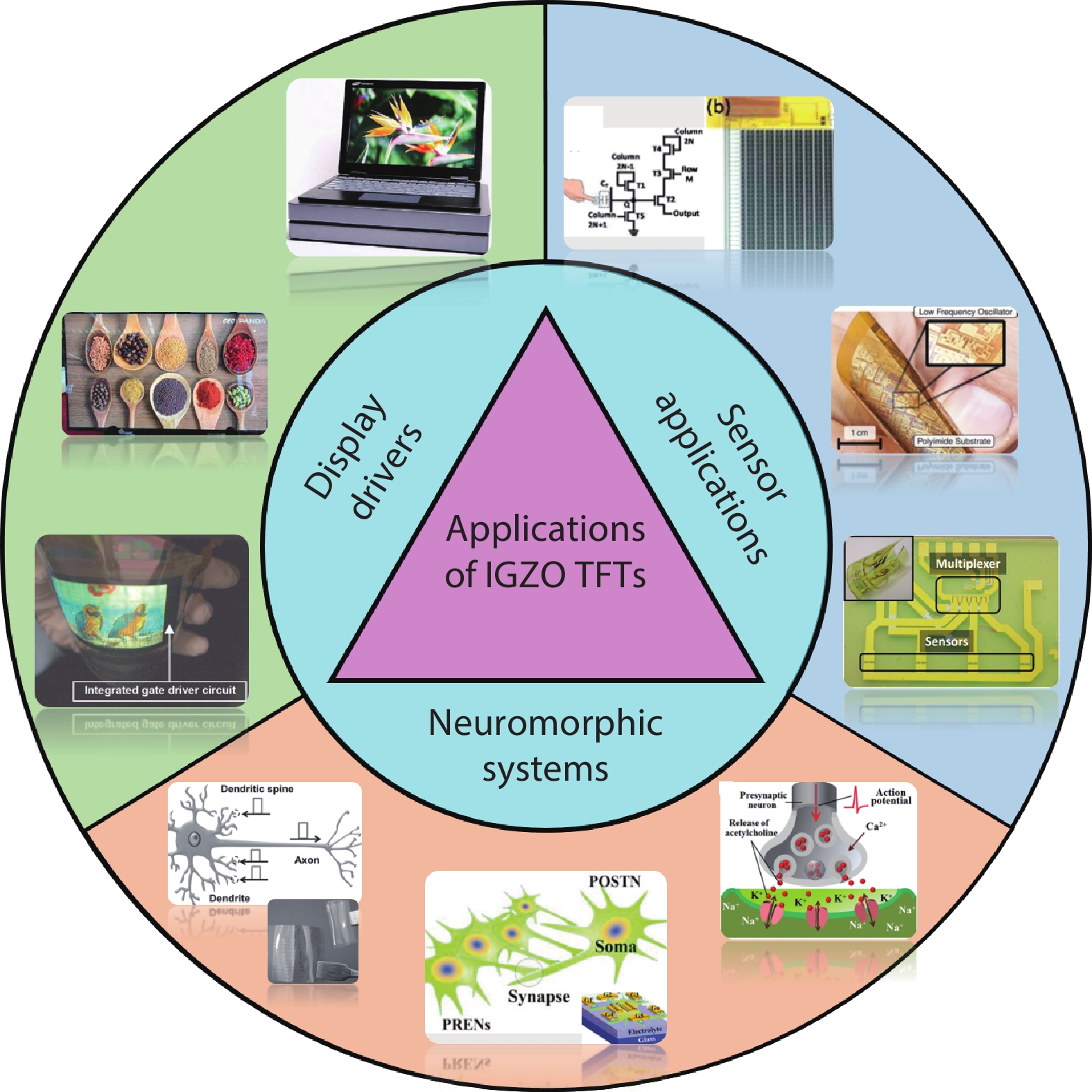
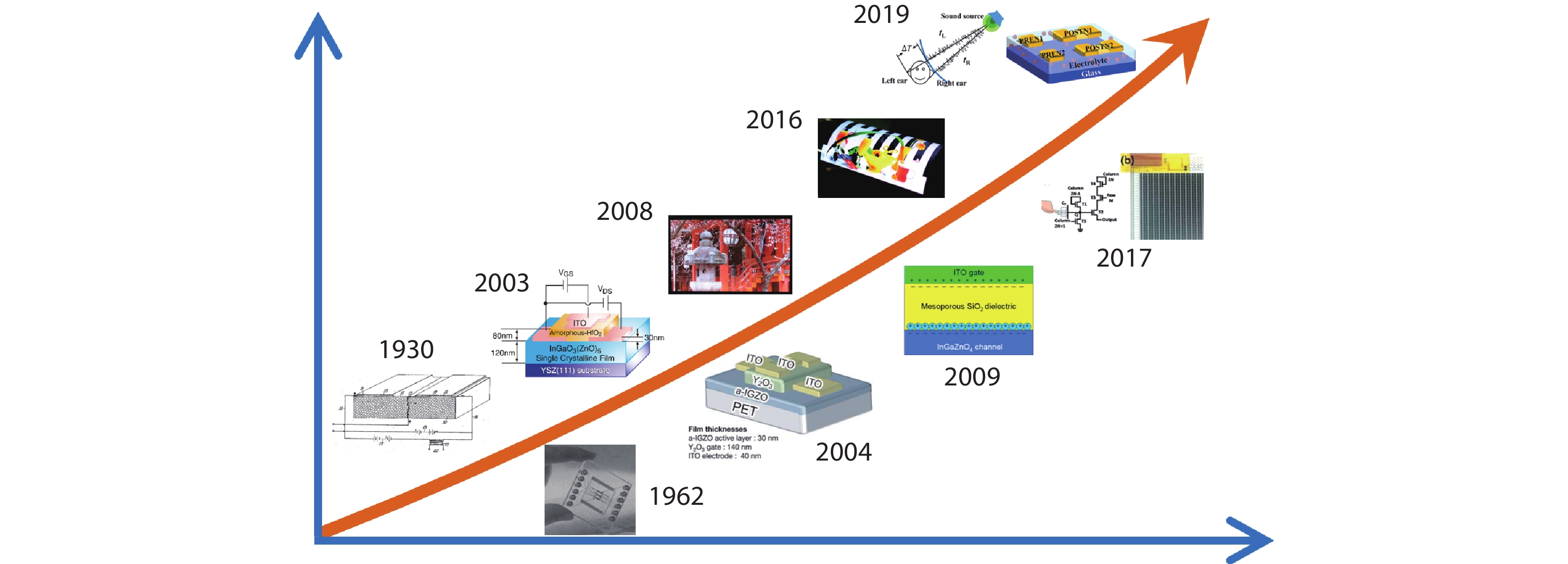
Since the invention of amorphous indium–gallium–zinc–oxide (IGZO) based thin-film transistors (TFTs) by Hideo Hosono in 2004, investigations on the topic of IGZO TFTs have been rapidly expanded thanks to their high electrical performance, large-area uniformity, and low processing temperature. This article reviews the recent progress and major trends in the field of IGZO-based TFTs. After a brief introduction of the history of IGZO and the main advantages of IGZO-based TFTs, an overview of IGZO materials and IGZO-based TFTs is given. In this part, IGZO material electron travelling orbitals and deposition methods are introduced, and the specific device structures and electrical performance are also presented. Afterwards, the recent advances of IGZO-based TFT applications are summarized, including flat panel display drivers, novel sensors, and emerging neuromorphic systems. In particular, the realization of flexible electronic systems is discussed. The last part of this review consists of the conclusions and gives an outlook over the field with a prediction for the future.

Key words: indium–gallium–zinc–oxidethin-film transistorsflat panel displayssensorsflexible electronicsneuromorphic systems

Metal oxide semiconductor thin-film transistors (TFTs), especially indium–gallium–zinc–oxide (IGZO)-based TFTs, have received considerable interest since Nomura et al. reported the first amorphous IGZO (a-IGZO) based TFT in 2004. Before the invention of the first a-IGZO-based TFT, the crystalline IGZO materials were first reported as early as 1985[1]. However, it was not until 2003 and 2004 that Nomura et al. used the IGZO materials of single-crystalline and amorphous states as the TFT semiconductor channel materials, respectively[2, 3]. The key advantage of single-crystalline is that there are no defects or grain boundaries, which makes TFTs with ultra-high mobility. However, a high temperature is needed for single crystal growth, which is not favorable for large-area application. In 2004, Nomura et al. reported that a-IGZO film can be deposited at low temperature. Now, a-IGZO films have become the most common TFT channel semiconductor materials. Compared to amorphous silicon TFTs with a field-effect mobility lower than 1.0 cm2/(V·s), a-IGZO-based TFTs usually show a field-effect mobility higher than 10 cm2/(V·s)[4-7].

Several well-known display companies (e.g., Sharp, Samsung Electronics, and LG Electronics) have demonstrated that IGZO-based TFTs have many potential applications in liquid crystal displays (LCDs), organic light emitting diodes (OLEDs) display and electronic paper displays[7-14]. In addition to flat panel displays, IGZO-based TFTs are also actively involved in sensor applications and neuromorphic systems. IGZO-based TFTs have the key advantages of distinguishable sensitivities to light, pressure, pH, gas, and some other parameters, which meet the requirements of these sensors. Furthermore, based on the relatively mature display technology, sensors with IGZO-based TFTs are easier to manufacture[15-30]. In particular, the IGZO-based TFTs show great potential in the field of flexible electronics because of their unique advantages of light-weight, ultrathin thickness and resistance to mechanical bending[13, 31-33]. IGZO-based TFTs with electrolyte gate dielectrics are very favorable for artificial synapse/neuron emulation, due to the interfacial electric-double-layer coupling and electrochemical doping effects[34-41]. IGZO-based TFTs neuromorphic devices show very low-energy consumption down to pJ/spike because of the extremely high gate capacitance of the electrolyte gate dielectrics and the high resistance of IGZO channel layers[42-45]. Some important applications of IGZO-based TFTs are shown in Fig. 1.

Figure  1.  (Color online) Some important applications of IGZO-based TFTs[11, 20, 3437, 4648].

With the rapid development of IGZO-based TFTs in various aspects of our life, especially in the field of display, a large number of studies based on the IGZO-based TFTs have been reported. Thus, this article aims to review the recent progress and the major trends in the field of IGZO-based TFTs. In this paper, we review the materials, devices and applications of IGZO-based TFTs. First, the history, electron travelling orbitals and deposition methods of the IGZO thin film are introduced. Second, we introduce the traditional devices and the new-concept device structures. Third, we comprehensively discuss the main applications, including display drivers, sensor applications and neuromorphic systems using IGZO-based TFTs. Finally, our conclusions and the outlook for IGZO-based TFTs are discussed.

Crystalline IGZO materials were first discovered by Kimizuka et al. in 1985[1]. These authors successfully fabricated InGaZnO4 with YbFe2O4-type structure by sintering at a temperature above 1000 °C. Until 2003 and 2004, the single-crystalline and amorphous state IGZO materials were proposed for TFT channel semiconductors by Nomura et al.[2, 3], respectively. In 2003, Nomura et al. presented a transparent TFT with single-crystalline IGZO thin film as the channel layer. The unique advantages of the single-crystalline InGaO3(ZnO)5 thin film are that there are no grain boundaries and defects, which enable the single-crystalline IGZO-based TFT to show a field-effect mobility (μFE) as high as ~80 cm2/(V·s). However, a high annealing temperature of 1400 °C was needed to form the single-crystalline phase. This high temperature process limited the practical application. In the next year, amorphous IGZO (a-IGZO) thin films were deposited at low temperature by Nomura et al.[3]. This a-IGZO thin film was prepared by pulsed laser deposition (PLD) using a polycrystalline InGaZnO4 ceramic target. The first a-IGZO-based TFT showed a saturation mobility of 6–9 cm2/(V·s), a current on/off ratio (Ion/Ioff) of 103 and threshold voltage (Vth) of 1.6 V.

The electron travelling orbitals of oxide semiconductors are different from covalent semiconductors. Covalent semiconductors (e.g., silicon) possess carrier transport paths of directive sp3 orbitals[3]. Thus, the electron mobility of single crystal silicon can reach up to 1000 cm2/(V·s)[38]. However, if the carrier conducting pathway was disrupted in the case that the crystalline structure was broken or under amorphous state, then the carrier mobility would be lower by three orders of magnitude than single crystal silicon[39]. Unlike covalent semiconductors, oxide semiconductors are of degenerate band conduction. Fig. 2 shows the carrier transport paths of crystalline and amorphous oxide semiconductors. The carrier transport paths of metal oxide semiconductors are composed of spatial metal ns orbitals with isotropic shape. Because s orbital is of spherical symmetric, the overlap in distorted metal–oxygen–metal can also offer a conductor pathway.

Figure  2.  (Color online) Carrier transport paths of (a) crystalline, (b) amorphous post-transition-metal oxide semiconductors[3].

Many methods have been proposed to deposit IGZO thin films. The most commonly used method is sputtering because it is compatible with uniform deposition on the large surface with low cost[40, 41, 49]. Pulsed laser deposition (PLD)[3], atomic layer deposition(ALD)[50-52], plasma enhanced chemical vapor deposition (PECVD)[53-55] and solution methods such as spin-coating, inkjet printing and gravure printing[56] are also used for IGZO-based TFT fabrication. These methods possess unique advantages, for example, IGZO thin film grown by ALD showed a roughness at the atomic level. The PECVD method can well control the reactive species concentration and further regulate the film deposition rate.

The first concept of thin-film transistors (TFTs) was patented as early as the 1930s[57]. However, TFTs were only at the concept stage without vacuum technology and an understanding of semiconductors. The first practical TFT was fabricated in 1962 by Weimer[58]. In his experiment, microcrystalline cadmium sulfide film was used as the semiconducting channel layer and silicon oxide was used as the gate dielectric. Since 2003, zinc oxide (ZnO) TFTs have attracted much interest[59-61]. However, ZnO films crystallize at low temperature and usually show polycrystalline structure, which is not suitable for large-area macroelectronics. Fortunately, Nomura et al. invented the first a-IGZO-based TFT in 2004[3]. IGZO-based TFTs have gradually gained practical applications thanks to their high electrical performance, large-area uniformity, and low processing temperature. Fig. 3 shows a time axis diagram of the development of the IGZO-based TFTs.

Figure  3.  (Color online) A time axis diagram of the development of the IGZO-based TFT[13, 11, 20, 36, 44, 57, 62].

Many possible device structures for IGZO-based TFTs are shown in Fig. 4[63, 64]. Figs. 4(a)4(e) show the bottom-gate structure, top-gate structure, dual-gate structure, vertical structure and multiple gate structure, respectively. Figs. 4(a) and 4(b) are the simplest device structures that require very few manufacturing steps, which are very friendly to the laboratory device preparation. For example, the structure in Fig. 4(a) just needs one lithographic step, which makes the device preparation relatively quick and cheap. However, the electrical properties of those devices are unstable because the channel materials are exposed to the atmosphere, and will be influenced by the moisture and oxygen in the air. In the dual-gate structure, just as the name implies, bottom gate and top gate are together used to control the device properties, such as the threshold voltage, subthreshold swing, current on/off ratio[65-68]. The devices of vertical structure possess small footprint, resistance to the bending stress and controllable channel length[69-71]. TFTs of multiple in-plane gate electrodes are used in neuro-transistors to simulate spatiotemporal information processing[72].

Figure  4.  (Color online) Schematic diagrams of the device structures with (a) bottom gate, (b) top gate, (c) double gate, (d) vertical and (e) multiple gates.

In IGZO-based TFTs, source/drain electrodes, gate electrode, gate dielectric and IGZO semiconductor channel material are used in the TFT structures. Electrodes are usually composed of metal materials, high conductive metal oxides and new materials such as graphene[70, 73, 74]. Various materials are used as gate dielectrics. First, traditional gate dielectrics like SiO2 and SiOx[66, 75], which can be compatible with traditional TFT fabrication process. Second, high κ materials, such as Al2O3, HfO2, ZrO2, Y2O3 and Ta2O5[50, 70, 76]. The advantages of these materials are that they can reduce the equivalent oxide thickness and decrease the device size. However, they are of poor interface quality and reduce compatibility with the TFT fabrication process. Third, organic gate dielectrics such as olefin polymers and polyvinyl pyrrolidone (PVP)[77, 78]. These organic gate dielectrics are usually used in the flexible electrics. Finally, ion gate dielectrics, such as proton conducting nanogranular SiO2 and chitosan[79, 80]. These dielectrics are actively used in the electric-double-layer TFTs and produce a large capacitance.

Sato et al. presented a bottom-gate type coplanar homojunction a-IGZO-based TFT[75]. In this work, they employed highly doped contact regions naturally formed by depositing upper protection layers made of hydrogenated silicon nitride. As a result, a nearly ideal Ohmic contact was formed with a low parasitic source-to-drain resistance of 34 Ω·cm. Fig. 5(a) shows a schematic diagram of the TFT structure. The device was fabricated on a glass substrate. The molybdenum (Mo) layer was sputtered as the bottom-gate electrode. The SiOx layer was deposited by PECVD as the gate dielectric. This gate dielectric material is commonly used because it is compatible with the traditional TFT fabrication process. Then, the a-IGZO semiconductor film was deposited by direct-current magnetron sputtering and used as channel layer at room temperature. SiOx/SiNx layer was deposited by PECVD and used as a protection layer. The region that was not covered SiOx after depositing SiOx/SiNx film was converted to highly conductive source/drain electrodes. Figs. 5(b) and 5(c) show the transfer and output curves of the TFTs, respectively. The device showed a good subthreshold swing (SS) of 0.13 V/decade, a Vth of 0.13 V, and an Ion/Ioff of over 109 at Vds = 10 V. From the output characteristics, we can see a steep rise in the low Vds region, which indicated a good Ohmic contact between semiconductive a-IGZO and source/drain electrode.

Figure  5.  (Color online) (a) Schematic diagram of the bottom-gate coplanar homojunction a-IGZO device structure. (b, c) Transfer and output curves of the device, respectively[75].

Zhang et al. proposed a self-aligned top-gate a-IGZO-based TFT with a thickness of 8.62 nm SiO2 as gate dielectric[74]. This device realized the ultrathin gate dielectric less than 10 nm with low leakage current. Fig. 6(a) shows the structure of the TFT and the major processing steps, respectively. A thickness of 40 nm a-IGZO thin film was deposited on the glass substrate by sputtering at room temperature. A thin SiO2 film with thickness lower than 10 nm was deposited as the gate dielectric by PECVD at 300 °C. The 80 nm thick Mo film was then deposited on the SiO2 layer and patterned to form the gate electrode by dry etching. Finally, the Mo layer was used as the source/drain electrodes by a lift-off process. Figs. 6(b) and 6(c) show the transfer and output characteristics of the a-IGZO-based TFT, respectively. The a-IGZO-based TFT showed a low off-state current of less than 10–12 A, a low gate leakage current of 10–13 A, a μFE of 10.13 cm2/(V·s), a Vth of 0.52 V and a high Ion/Ioff over 108 at Vds = 2.1 V. Such a-IGZO TFTs with ultrathin SiO2 gate dielectric have achieved a low gate leakage current and have also shown a good electrical stability under positive and negative gate bias stresses.

Figure  6.  (Color online) (a) Schematic diagram of the top-gate a-IGZO-based TFT structure and the major processing steps, respectively. (c, d) Transfer and output curves of the a-IGZO-based TFT, respectively[74].

In the dual-gate structure, the top gate and bottom gate are together used to modulate the channel carrier concentration and further control the electrical performance of the device, such as the turn-on voltage, the threshold voltage and the field-effect mobility, through applying voltage to the bottom and top-gate electrodes[81-84]. The work principle of dual-gate TFT is somewhat like that of the single-gate TFT, utilizing the electric field capacitively to control the channel. By changing the polarity or amplitude of the voltage applied to the bottom or the top gate, the channel actually becomes enhanced or depleted. The concentration of the conductive carriers (the majority carriers) changes and the electrical performance of the device can also be modulated. Li et al. presented a comparison between the single-gate and dual-gate TFTs[66]. Figs. 7(a) and 7(b) show the schematic structures of the single-gate and dual-gate devices, respectively. The a-IGZO thin film was deposited as the channel layer by reactive sputtering. Figs. 7(c) and 7(d) show the transfer and output curves of the single-gate TFT, respectively. Figs. 7(e) and 7(f) show the transfer and output curves of the dual-gate TFT, respectively. Compared with the single-gate TFT, the performance of the dual-gate TFT is more superior. The on current was 2.54 times higher than that of the single-gate TFT, the μFE was about 1.23 times higher than that of the single-gate TFT, and SS was about half of the single-gate TFT.

Figure  7.  (Color online) Schematic diagrams of the structures of (a) single-gate and (b) dual-gate TFT, respectively. (c, d) Transfer and output curves of the single-gate device, respectively. (e, f) Transfer and output curves of the dual-gate device, respectively[66].

Vertical structure devices can offer ultrashort channel with high current. Furthermore, the ultrashort channel enables the device to resist mechanical stress, which is especially important for flexible devices[70]. In planar IGZO-based TFTs, a few cracks in the IGZO thin film can severely degrade the migration of the carriers. However, in vertical structures, the vertical current is unaffected by planar cracks. When the device suffers an external mechanical stress, usually causing several cracks across the IGZO thin film, as shown in Fig. 8(d), the TFTs in the vertical structure are less affected because the current transfer between the source and drain is in the vertical direction. Liu et al. presented a highly flexible vertical TFT with the IGZO thin film as the channel layer[70]. Fig. 8 shows the vertical device structure and the charge transport paths in the planar and vertical TFTs, respectively. The structure of the vertical TFTs is based on the vertical heterostructure of graphene-IGZO-metal stack. Tanium (Ti) was sputtered as the drain electrode. The IGZO thin film was deposited as the channel layer. The chemical vapor deposition (CVD) graphene was transferred onto the IGZO thin film as the source electrode. A thickness of 40 nm Al2O3 thin film was deposited on the top of the channel as the gate dielectric with high dielectric constant. When the cracks appeared in the IGZO thin film, as shown in Figs. 8(c) and 8(d), the carriers cannot be transported in the planar structure because the source/drain electrodes are both in the same plane and the current is blocked by the cracks. However, as shown in Figs. 8(a) and 8(b), the source/drain electrode and gate electrode are in the vertical direction, and thus the carrier transfer are less affected. Based on the characteristics of the resistance to mechanical stress, these vertical structure TFTs are significantly favorable for the application of flexible electronics.

Figure  8.  (Color online) (a, b) Schematic diagrams of the vertical IGZO-based TFT structures. (c, d) Carriers transferred in the planar and vertical TFTs with cracks in the IGZO thin film, respectively[70].

In 2017, IGZO-based neuron TFTs with multiple in-plane gate electrodes were reported by our group[72]. Fig. 9 shows the device structure of the neuron TFTs gated by a nanogranular SiO2 electrolyte film. Electric-double-layer effect due to the mobile proton in the SiO2 electrolyte film provided a very large specific gate capacitance. Voltage pulses applied on the in-plane gate electrodes can be temporally and spatially coupled to the IGZO channel layer due to the indium–zinc–oxide (IZO) floating gate. These IGZO-based neuron TFTs are favorable for sensors and neuromorphic applications.

Figure  9.  (Color online) Schematic diagram of the IGZO-based neuron TFTs with multi-gate structure[72].

IGZO-based TFTs have been applied in many areas, such as display drivers, sensors and neuromorphic systems[10, 23, 25, 85-88]. In this section, we will introduce the important applications based on IGZO-based TFTs in commercial production and scientific research.

Hydrogenated amorphous silicon (a-Si:H) and low-temperature polysilicon (LTPS) have been widely used in practical displays. However, the electron mobility of a-Si:H is usually low (1.0 cm2/(V·s)) and the TFTs are unstable under stress and illumination[4]. LTPS TFTs possess high mobility and good stability compared to a-Si:H TFTs[11]. Nevertheless, the process cost of preparing LTPS films is relatively high, especially for large-size displays[4, 5, 85, 89]. In addition to these two materials, the IGZO thin film has the advantages of high electron mobility, low-temperature fabrication process, high uniformity of large area and low cost. These advantages ensure that the IGZO-based TFTs are favorable for the applications of displays[9, 11-13, 31, 41, 85, 90-103].

LCDs are a relatively mature technology and are used in display panels, such as smart phone displays, tablet personal computers and televisions. The trends of LCDs are high resolution (7680 × 4320 pixels), ultra-high pixel density of over 300-ppi (pixels per inch) and refresh rate of 240 Hz or higher. To follow these trends, smaller and faster TFTs are required. Consequently, a-IGZO-based TFTs are considered as an advanced method to achieve the high pixel density on a large panel size, due to their high mobility and small size. For example, Baek et al. reported a dual-gate synchronized a-IGZO-based TFT for the application of an active-matrix liquid crystal display (AMLCD)[91]. To understand the operation principle of the dual-gate a-IGZO-based TFT under synchronized bias conditions, a mathematical analysis of the dual-gate synchronized a-IGZO-based TFT is analyzed in this work. The equation of current in saturation region is IDS = WμC(VGSVTH)2/2L, and the equation of subthreshold swing is SS = (∂ log10IDS/∂ VGS)–1, where W and L are the channel width and length, C is the capacitance of the channel semiconductor, and μ is field-effect mobility. Compared with the top-gate, bottom-gate, and synchronized dual-gate a-IGZO TFTs only by bias conditions, from the calculations, the dual-gate a-IGZO-based TFTs under synchronized bias produced larger current and steeper SS compared to the single-gate TFTs with the same channel width/length ratio. These superior properties of the a-IGZO-based TFTs allow the AMLCD to have high pixel density and high resolution. Fig. 10 shows the proposed pixel circuit with the synchronized dual-gate a-IGZO-based TFT for the AMLCD. In the pixel, the switching transistor (a-IGZO-based TFT) was of an inverted staggered structure with an additional gate electrode (top gate). Furthermore, the top gate and the bottom gate were tied together through the sync via, which prevented the dual-gate TFTs from suffering the degradations of the mobility and subthreshold swing. These a-IGZO-based TFTs achieved a smaller size for the same amplitude of drain current.

Figure  10.  (Color online) Pixel circuit of the AMLCD based on synchronized dual-gate a-IGZO-based TFTs[91].

OLEDs driven by a-IGZO-based TFTs are still in the development stage and they have not been put into the display market on a large scale. For further development, crucial problems such as device stability, imaging uniformity and yield[104-108] need to be solved urgently. For example, the threshold voltage of the a-IGZO-based TFT usually shifts under electrical bias stress[108], which would cause non-uniform brightness in the OLED displays. Fortunately, TFTs with dual-gate structure can control the threshold voltage with little variation[101]. Wang et al. reported a dual-gate a-IGZO-based TFT-driven pixel circuit for active-matrix OLEDs (AMOLEDs)[101]. Figs. 11(a) and 11(b) show schematic diagram and the electrode definition of the dual-gate TFT structure, respectively. The bottom gate and the top gate were defined as the primary gate and the auxiliary gate, respectively. The threshold voltage of the dual-gate TFT under the primary gate operation can be modulated by the auxiliary gate voltage. Fig. 11(c) shows the transfer curves of the dual-gate a-IGZO-based TFTs under the primary gate operation with auxiliary gate voltage changing from –4 to 4 V. As shown in Fig. 11(d), the threshold voltage shifted linearly with the auxiliary gate voltage. Therefore, the Vth variation under the primary gate operation could be compensated by varying auxiliary gate voltage. Fig. 11(e) shows a schematic of the pixel circuit including one driving TFT (T1), four switching TFTs (T2–T5) and two capacitors (C1 and C2).

Figure  11.  (Color online) (a) Schematic diagram of the measured dual-gate a-IGZO-based TFT structure. (b) Definition of the electrodes. (c) Transfer curves of the dual-gate a-IGZO-based TFT under primary gate operation with auxiliary gate voltage changing from –4 to 4 V. (d) Threshold voltage as a function of auxiliary gate voltage. (e) Structure of the pixel circuit[101].

Flexible IGZO-based TFTs are capable for use as flexible displays, due to the unique advantages such as light-weight substrates[87, 109-112], low-voltage-driven[113], and bendability[114, 115]. In addition, when the IGZO thin films are deposited on to suitable substrates, the IGZO-based TFTs can be used to form fully transparent flexible displays. Flexible displays driven by IGZO-based TFTs have been researched in many works[13, 31, 34, 116]. For example, in 2009, Park et al. fabricated a 6.5 inch full-color flexible AMOLED on the polyimide (PI) substrate driven by a-IGZO-based TFTs[13]. The a-IGZO-based TFT showed a Vth of 0.9 V, an SS of 0.25 V/dec, a μFE of 15.1 cm2/(V·s). Moreover, there was no performance degradation under bending of the R = 3 mm. Nag et al. presented a top-emitting quarter-quarter-video-graphics-array AMOLED display with 85-ppi resolution driven by a-IGZO-based TFTs[31]. In this display panel, the driven a-IGZO-based TFT showed high electronic characteristics of μFE of 12.0 cm2/(V·s), SS of 0.5 V/dec, and Ion/Ioff of over 107.

Most TFT gate drivers integrated on the display panel use carry signals between the stages. However, in the flexible display the error of the stressed stages is accumulated through the carry signals when the display panel is bent. This problem will probably lead to the failure of the image refresh. To deal with this problem, Kim et al. reported a carry-free gate driver for flexible displays using a-IGZO-based TFTs[117]. This carry-free gate driver overcame that problem because it did not use the carry signals and each unit stage operated independently. Fig. 12(a) shows the conceptual architecture and the output waveforms of the carry-free gate driver. Each unit stage works as a decoder and the output of each stage is decided by the binary-weighted decoder signals. When the mechanical stress is applied, the outputs of the stressed stages would become slower but the errors could not accumulate because there are no carry signals through which the error can propagate and each stage works independently. As shown in Fig. 12(b), the flexible display with a carry-free gate driver can keep the normal operation, even under the mechanical stress. Moreover, the carry-free gate driver showed no voltage fluctuation at the outputs after 10 000 cycles bending test with a bending radius of 2 mm. These carry-free gate drivers achieve high reliability under mechanical stress compared with the traditional carry-type gate drivers for flexible displays.

Figure  12.  (Color online) Conceptual architecture and flexible display panel with carry-free gate driver[117].

Table 1 shows the recent studies of the display applications driven by the a-IGZO-based TFTs. This table shows the substrate, structure, electrical properties of the a-IGZO-based TFTs, the size of the display panel and the specific application.

Table  1.  Display applications of the IGZO-based TFTs.
SubstrateStructure of the TFTμFE (cm2/(V·s))Vth (V)SS (V/dec)Size (inch)ApplicationRef.
GlassDual-gate110.2413055LCD[118]
GlassInverted stagger932LCD[48]
GlassBottom gate153.20.480LCD[104]
GlassInverted bottom gate4.2±0.4–1.30.96±0.115AMLCD[12]
GlassBack channel etch7.351.6AMLED[100]
GlassStaggered bottom gate8.21.10.5812.1AMOLED[11]
18.451.040.73AMOLED[97]
GlassEtch stopper204.8AMOLED[103]
PolyimideStaggered bottom gate17.30.860.2111.7Flexible AMOLED[119]
PolyimideInverted staggered bottom gate11.61.60.253Flexible AMOLED[34]
PolyimideCoplanar10.250.340.22Flexible OLED[120]
DownLoad: CSV  | Show Table

Nowadays, a-IGZO-based TFTs have attracted considerable attention thanks to their large-size, high-resolution and narrow-bezel display applications. Fig. 13 shows this progress in display applications. For example, China Star Optoelectronics Technology (CSOT) developed an 85-inch 8k4k LCD driven by the IGZO-based TFTs. The large-size LCD panel is shown in Fig. 13(a)[121]. Fig. 13(b) shows a 1058-ppi ultra-high-resolution flexible OLED display using IGZO-based TFTs fabricated by Semiconductor Energy Laboratory[62]. Usually, in the display market, displays with a pixel of about 400-ppi are used. This OLED display showed an ultra-high resolution of 1058-ppi with c-axis-aligned nanocrystalline IGZO materials and could be used for mass production. LG Display demonstrated a bezel free designed AMOLED driven by a-IGZO-based TFTs in 2019[122]. Fig. 13(c) shows an image of the panel. In the fabrication process, this panel is designed to be bezel free. The small remaining bezel of 0.x mm is shown in Fig. 13(c), due to the panel cutting process from the mother glass. We believe that in the future displays driven by the IGZO-based TFTs will gradually occupy a dominant position not only in the field of LCD or OELD but also in the field of true flexible displays.

Figure  13.  (Color online) Picture images of the display panels of large size, high-resolution and narrow bezel[62, 121, 122].

Sensors can detect the light, force, voice, gas, humidity et al. and transfer them into electrical signal. At present, sensors have been applied in industrial manufacture, healthcare monitoring[123], food safety[124], artificial electronic skins and so on. IGZO-based TFTs are compatible with semiconductor integrated circuit technology and they possess the advantages of small size, room-temperature fabrication process and sensitivity to the pH, pressure, light, gas and so on[16, 20, 22, 23, 25, 125-128], which meet with the requirements of the sensors. In this section, we will present the main sensor applications based on the IGZO-based TFTs.

Photodetectors have attracted increasing attention, due to their wide applications in biomedicine, fire monitoring, photo-communication, missile plume detection and so on. The photodetectors based on the IGZO-based TFTs exhibit a relatively high response to light with a wavelength lower than 420 nm because the IGZO materials possess a wide bandgap over 3.0 eV. For example, Yu et al. presented an ultraviolet (UV) photodetector based on the IGZO-based TFT with a p–n junction[27]. Fig. 14 shows a schematic diagram of the IGZO-based TFT structure, the carrier transmission process under the light and the photo responsivity of the IGZO and PEDOT:PSS/SnOx/IGZO TFTs, respectively. The p–n junction was composed of the PEDOT:PSS/SnOx/IGZO heterojunction structure. Through the p–n junction, the directional carrier transfer of the photo-generated carriers was experimentally validated. A photo responsivity of 984 A/W at a wavelength of 320 nm was obtained in this work. This work has successfully fabricated a visible-blind ultraviolet photodetector based on the a-IGZO TFTs and achieved ultra-low-power dissipation of lower than 10 nW under illumination and about 0.2 pW in the dark. Moreover, this photodetector with high photoresponsivity has the unique advantage of pixel integration, which can potentially be applied in high performance visible-blind ultraviolet photodetector pixel arrays. Besides the UV photoelectric sensors, the IGZO-based TFTs with narrow-bandgap materials such as graphene dots[129], silver nanoparticles[130] and polymer[131] have successfully been used in visible-light photoelectric sensors. For example, in 2010, Zan et al. demonstrated a visible-light phototransistor that consisted of a wide-bandgap a-IGZO and a narrow-bandgap (about 2 V) poly (3-hexylthiophene) (P3HT)[131]. The a-IGZO thin film and P3HT formed a p–n junction diode. The P3HT layer has a high absorption coefficient for visible light and absolutely absorbs visible light, and consequently injects electrons into the a-IGZO layer. As a result, the concentration of the carriers in the channel and also the threshold voltage of the a-IGZO-based TFT change rapidly with the illumination. In this work, the authors proposed a simple way to convert a wide-bandgap a-IGZO-based TFT into a visible-light photodetector that has a fast response and a high sensitivity. Although ultraviolet and visible-light phototransistors have been fabricated in many works, there are few reports of infrared photodetectors based on IGZO TFTs. Lee et al. for the first time characterized the infrared photoresponse principle through the subgap density-of-states over the forbidden bandgap of a-IGZO[26]. The origin of the sub-bandgap ( < Eg) photo response in a-IGZO-based TFTs was that the electrons were optically pumped from the photo-responsive sub-bandgap states. From these works, we can see that the photodetectors based on the IGZO-based TFTs have been investigated from ultraviolet to infrared. These works provide useful results that can help the integration of the photodetectors based on the IGZO-based TFTs.

Figure  14.  (Color online) (a) A schematic diagram of the IGZO-based TFT structure. (b) The separation and collection process of the photo-generated carriers. (c) Photoresponse of the IGZO and PEDOT:PSS/SnOx/IGZO phototransistors as a function of the light wavelength[27].

Pressure sensors are used to monitor pressure magnitude and fluctuation, which are important in areas such as blood flow, heartbeat, and respiratory system of the human body[132]. Piezoelectric sensors have attracted much attention because they can generate an electric potential in response to an applied pressure. Geng et al. proposed a pressure sensor based on a dual-gate a-IGZO-based TFT with a polyvinylidene fluoride (PVDF) piezo-capacitor[133]. When the pressure is applied by finger pressing, the potential of the top-gate will change, thus the threshold voltage of the a-IGZO TFT shifts, which will produce an obvious output signal in the range of 200–300 mV. Fig. 15(a) shows the structure of a dual-gate a-IGZO-based TFT with a piezo-capacitor. The unique advantage of the double gate structure is that the electrical characteristics of the TFT can be simultaneously controlled both by the bottom gate and top gate. In this structure, the piezo-capacitor was formed on the top of a floating top gate. The piezo-capacitor was polarized and generated a voltage to the top gate when it was pressed. Fig. 15(b) shows the transfer curves of the dual-gate a-IGZO-based TFT. From the curves, the Vth of the dual-gate a-IGZO-based TFTs shifted to the positive bottom-gate voltage direction by applying negative top-gate voltage, and to the negative bottom-gate voltage direction by applying a positive top-gate voltage. Moreover, the Vth would return to its initial value after removing the top-gate voltage. This change of the Vth with different top-gate voltage is the mechanism of the pressure sensors. This work has realized a pressure sensor using piezo-capacitor that integrated with dual-gate a-IGZO-based TFTs.

Figure  15.  (Color online) (a) Schematic diagram of the a-IGZO-based TFT pressure sensor structure. (b) Transfer characteristics of the dual-gate TFT with different top-gate voltage[133].

Biosensors have attracted considerable interest for disease diagnosis and the pursuit of a better life. In particular, pH sensors play an important role in clinical medicine, environmental monitoring, agriculture and food engineering[18, 134, 135]. IGZO-based TFTs possess the advantages of compatibility with flexible substrates, chemical/electrical stability and micro/nano size, which are satisfied with the pH sensors[19, 136]. For example, Smith et al. presented a flexible extended-gate ion-sensitive field-effect transistor (ISFET) biosensor based on the IGZO-based TFTs using LED technology[19]. The ISFETs are well used as pH sensitive biosensors with different dielectrics such as SnO2[136], TiO2[126] and ITO[19] as the pH sensitive layers[18, 125]. In this work, the ISFET drain current was increased as the pH decreased, which was due to the H+ ion protonation of the ITO extended-gate electrode surface. When the H+ concentration increased around the surface of the ITO gate electrode, negative charge carriers in the channel were generated thanks to the increased positive charge at the ITO/IGZO interface with decreasing pH value, resulting in the increase of the drain current. Fig. 16(a) shows the structure of a flexible ISFET pH sensor. In this structure, a flexible 125 μm thick polyethylene naphthalate (PEN) plastic was used as the substrate. The top 1 × 3 mm2 indium tin oxide (ITO) layer was used as the extended gate to detect the pH value. A width/length = 9/9 μm IGZO layer was used as the n-channel. Fig. 16(b) shows the graph of the ISFET drain current vs time. A sequence of pH 4→ pH 7 → pH 10 → pH 7 → pH 4 with the interval of 400 s for each pH concentration was used to test the current. The current was tested from 0 to 10 s, 200 to 210 s, 400 to 410 s. As the pH concentration increased from pH 4 to pH 10, the drain current decreased because of the decrease of the H+ ion protonation in the ITO extended-gate electrode surface. These results of sensors fabricated on a flexible substrate demonstrate the initial possibility of directly using the flexible LED technology to produce low cost, good performance and flexible IGZO TFT-based biosensors.

Figure  16.  (Color online) (a) Structure of the flexible extended-gate ISFET pH sensor. (b) Data graph of the drain current vs time[19].

Gas sensors based on IGZO-based TFTs are used to detect both oxidizing and reducing gases (like NO2 and H2)[29, 137-139]. Oxidizing or reducing gas molecules act like electron acceptors or donors to change the carrier concentration, respectively, and thus change the drain current of the IGZO-based TFTs[30]. For example, Lee et al. reported a H2 sensor using the IGZO-based TFTs[138]. Palladium (Pd) was used as source/drain electrodes and also used to detect hydrogen (H2) gas concentration. The drain current increased as the Pd and IGZO interface barrier height decreased, which happened because of the formation of a hydrogen dipole layer at the interface[139]. To sense the reducing gas, Kim et al. presented a low-concentration NO2 gas detector. The a-IGZO thin film was used both as a channel and as a sensing layer[137]. Fig. 17 shows the device structure, transfer curves under 50 ppm NO2 gas concentration with different times, and the drain current change as a function of the exposure time, respectively. The threshold voltage positive shifted with an oxidation reaction in the NO2 gas, NO2 (gas) + e (surface of oxide) → NO 2 (adsorbed). In particular, the sensing data was accurately obtained from the variation of the drain current and this sensor achieved efficient detection of the variation of the NO2 concentration. Thus, a-IGZO TFT-based gas sensors show good responsivity, sensitivity and recovery from the low concentration of the NO2 gas.

Figure  17.  (Color online) (a) Schematic diagram of the IGZO-based TFT structure. (b) Transfer curves with different time under 50 ppm NO2 gas concentration. (c) Drain current vs time under 50 ppm NO2 gas concentration[137].

IGZO-based TFT sensors have been widely used in flexible light detectors, pH sensors, gas detectors, and so on[19, 22, 33, 140]. For example, Xin et al. presented a novel pressure-sensing system using an a-IGZO-based TFT configuration comprised of a microstructured polydimethylsiloxane (PDMS) capacitor[22]. Fig. 18 shows the structures and the output curves, respectively. This array was fabricated on a highly flexible PI substrate using the back channel etch structure. The mechanism of the device can be explained by the change of the capacitance of the microstructured PDMS under an external pressure to modulate the gate voltage and change the output drain current. This device shows sufficient sensitivity to detect pressure difference under extremely low-pressure regime. The microstructure PDMS thin film showed good sensitivity of 0.1 kPa–1 and response time of lower than 190 ms for the pressure of 12 kPa. According to the amplification effect of the a-IGZO-based TFT, the device showed a high sensitivity in the subthreshold region for the ultra-low-pressure (≤ 1.5 kPa) detection and good linearity in the linear region for low-pressure (≤ 7 kPa) detection. The results demonstrated that a novel approach can be used for pressure-sensing intelligent products.

Figure  18.  (Color online) Schematic diagrams of the a-IGZO-based TFT pressure-sensing system and output curves[22].

Flexible IGZO-based TFTs are especially capable for use as flexible circuits, such as oscillators, inverters, radio frequency identifications, operational amplifiers and clock generators[87, 141-143]. Thus, flexible sensors provided by flexible circuits have aroused a great deal of interest[47, 144]. For example, Meister et al. reported a low-power low-frequency light-sensing oscillator with IGZO-based TFTs that were integrated on a bendable plastic substrate[47]. This oscillator could be directly used as a light sensor without additional read out circuits. The device oscillated between 5 Hz in the dark and 31 Hz under daylight. The light-sensitivity of the oscillation frequency is between 7.4 Hz/klx in the dark and about 1.7 Hz/klx in the daylight. In particular, this device had a low frequency of 5–31 Hz and low power of 188 μW. Significantly, this work achieved a low-power consumption, flexible integrated circuit that can be directly used to sense the light intensity through the frequency of the oscillation in a small chip area.

Table 2 shows the recent studies of the sensor applications based on the IGZO-based TFTs. This table shows the substrate, structure, electrical properties and the specific sensor applications of the IGZO-based TFTs.

Table  2.  Sensor applications of the IGZO-based TFTs.
SubstrateStructure of the TFTμFE (cm2V–1s–1)Ion/IoffVth (V)SS (V/dec)ApplicationRef.
SiO2/SiTop gate18~1060.60.07Photoelectric sensor[145]
SiBottom gate10.82.30.34Phototransistor[131]
GlassBottom-gate31.08 × 1050.50.49Deep-ultraviolet phototransistor[146]
SiO2/SiDouble gate6.515 × 1060.510.12PH sensor[136]
SiDouble gate41072.80.31PH sensor[126]
SiO2/SiBottom gate7.58~1070.49Gas sensor[147]
Double gate13.82.9 × 1060.720.19Hybrid gas sensor[30]
GlassBottom gate121.39–1.920.24Temperature sensor[16]
Metal foilBottom gate21~1077.361.12Flexible thermal and pressure sensor[148]
PolyimideBack channel etch201071Flexible pressure sensor[149]
Polyethylene naphthalateBottom-gateBiosensor[19]
PolyethylenenaphthalateBottom-gate staggered10~1520.3Flexible X-Ray detector[150]
PolyimideBottom-gate inverted staggered13.340.87Flexible gas sensor[140]
DownLoad: CSV  | Show Table

Traditional computers based on von Neumann architectures play essential roles in almost every field and have led to the development of information technology. However, there are two main problems that hinder the further improvement of computing power: the first is the limitation on energy efficiency as we approach the end of the Moore’s law and the second is the challenge of the von Neumann bottleneck. According to Moore’s law, device size was made smaller and smaller. However, at present, the device size is close to the physical limit and Moore’s law is gradually failing. Meanwhile, information processing in the von Neumann computer requires the transmission between processor and memory units, which is unfavorable for computational efficiency and the size of the architecture. As computing speed increases, the energy consumption becomes larger. In the famous man-machine battle, the power of the artificial intelligence AlphaGo is about 150 kW. These problems of von Neumann computers will become more serious with the spread of the Internet of Things and artificial intelligence. As an efficient solution for complex data processing, neuromorphic electronics that emulate the functions and the information processing of the human brain have been proposed.

The human brain is a highly efficient computing system that can process input information and react to external stimuli with ultralow energy consumption of ~20 W and small volume occupation of ~1200 cm3 [151]. Neurons are often considered as the computational engines of the human brain. The signals conducted between neurons depend on the recent activities at either or both sides of the synapse. The connection strength between synapses is known as synaptic plasticity. Synaptic plasticity consists of three different styles: 1) long-term plasticity, in which the change of synapses can last for hours or longer and is considered to be memory; 2) homeostatic plasticity, which keeps the neurons in an appropriate state; and 3) short-term plasticity, in which the signals that occur in the synapses last for milliseconds or minutes, and is considered as a critical computational function in neural systems. Synapses are the basic units of computing and learning in the human brain. To build artificial neuromorphic systems inspired by the human brain, the basic requirement is to prepare a device that can simulate synaptic behaviors. In the past few years, complementary metal oxide semiconductor (CMOS) integrated circuits have been used to mimic the synaptic functions, such as IBM’s TrueNorth chip that integrated 5.4 billion transistors to simulate 1 million neurons and 256 million synapses[152]. However, large-scale CMOS-based analog circuits consume a large amount of energy, which hinders the development of the CMOS synaptic applications. In recent years, the design of a single device that mimics synaptic functions has received a lot of attention, such as two-terminal memristors[153-156]. Two-terminal memristors consist of three layers, two electrodes for sending and receiving information, and a ‘storage’ layer between them to memorize the information. Although two-terminal memristors possess the advantages of small size, simple device structure and low-energy consumption, the instability of the device and the integration difficulty may hinder their application in neuromorphic systems. Recently, three-/multi-terminal transistors have attracted much attention[157]. Unlike two-terminal memristors, these transistors have a gate to control the channel conductance and the energy consumption of the device can be lower. Furthermore, three-/multi-terminal transistors have good stability, controllable parameters and easy integration. For the emulation of synaptic behaviors, as shown in Fig. 19, the gate electrode is used as the presynaptic terminal and the channel layer with source/drain electrodes is considered as the postsynaptic terminal. The information transmission and process in the synapse starts from the triggering of the presynaptic pulse. Then, electrical activities in the pre-synapse are converted to the release of neurotransmitters and the post-synapse receives the neurotransmitters. Consequently, the current/potential of the post-synapse is changed. When a pulse voltage is applied to the gate electrode, the conductance of the channel layer is changed, which can be measured by applying a small voltage between the source and drain electrodes.

Figure  19.  (Color online) Schematic diagram of an artificial synapse based on neuromorphic transistor.

Herein, we will demonstrate the works reported by our group about the application of IGZO-based TFT in synaptic networks and neuromorphic systems[35-37, 42, 43, 45, 158-161]. As early as 2009, Jiang and Wan et al. reported the first ultralow-voltage IGZO-based electric-double-layer (EDL) TFT[44]. This TFT exhibited an ultralow operation voltage about 1.0 V, a high μFE of 28.5 cm2/(V·s), and a low SS of 110 mV/decade. This ultralow-voltage operation was ascribed to the large EDL capacitance. Usually, in a liquid or solid electrolyte, mobile cations and anions are filled between two electrodes. When an external voltage is applied to the electrodes, the cations and anions will move to the surface of electrolyte/electrode, respectively, which is the charging process and will contribute a large EDL capacitance[162]. In our work, the proton H+ in mesoporous SiO2 moved from one bridging oxygen atom to another. When a negative dc voltage was applied to the gate electrode, the H+ would move to the dielectric/channel interface. Simultaneously, the electrons in the n-type IGZO channel accumulated near the interface, due to the combination of the gate potential bias. Importantly, this work laid a solid foundation for the follow-up research of IGZO-based TFT artificial synapse devices.

It is essential for synaptic transistors to have low-energy consumption. Zhou and Wan et al. presented flexible EDL IGZO-based TFTs with the energy consumption as low as 0.23 pJ/spike[161]. In this work, short-term synaptic plasticity and high-pass filtering behaviors are also mimicked. Figs. 20(a) and 20(b) show the structure of the device and a simple image of the artificial synapse, respectively. The artificial synapse is composed of an IGZO transistor. The gate is considered as the pre-synapse and the channel is considered as the post-synapse. When the voltage pulse is applied to the gate, a spike could be measured in the drain electrode, which simulates the information transfer process in the synapse. Fig. 20(c) shows the paired-pulse facilitation (PPF) curve that the excitatory postsynaptic current (EPSC) triggered by a pair of gate voltage spikes. The PPF reached a maximum value of 192% when the time interval was 20 ms, and it was reduced to 100% because the time interval is long enough. When the time interval between the pair of gate voltage spikes is shorter than the relaxation time of the protons in the nanogranular P-doped SiO2, some of the protons could not diffuse back to their equilibrium position before the second spike arrives, causing a large PPF. However, with the increase of the interval time, the protons gradually move back to their equilibrium position and the PPF gradually decreases. Fig. 20(d) shows the EPSC amplitude gain as a function of spike frequency. As the frequency of the voltage train changed from 1 to 50 Hz, the gain increased from ~1.0 to ~3.7. These results demonstrate the high-pass synaptic dynamic filtering of the IGZO-based neuromorphic TFTs.

Figure  20.  (Color online) (a) Schematic diagram of the electric-double-layer (EDL) IGZO-based neuromorphic TFT structure. (b) Simple schematic diagram of an artificial synapse based on the IGZO-based TFT. (c) PPF ratio as a function of the time interval between the two stimuli spike. (d) EPSC amplitude gain as a function of spike frequency[161].

Emulation of the short-term synaptic plasticity and synaptic filtering based on IGZO-based EDL TFTs was proposed by Wan et al.[45]. To simulate the synaptic facilitation and depression function, a three-terminal device was reduced to a two-terminal synaptic device. High-pass and low-pass filtering were successfully simulated. Figs. 21(a) and 21(b) show schematic images of the IGZO-based EDL TFT. In Fig. 21(a), the drain electrode and gate electrode were shortly connected as the presynaptic terminal. When we applied a positive voltage to the drain electrode, the protons in the electrolyte migrated to the IGZO channel/electrolyte interface. The EPSC was increased and the facilitation simulation was achieved. Fig. 21(b) shows that the source electrode and gate electrode were shortly connected as post-synapse terminal to emulate the short-term depression behavior. When the positive spike was applied to the drain electrode, the protons in the electrolyte migrated to gate electrode/electrolyte interface. The response current gradually reduced and synaptic depression can be obtained. Figs. 21(c) and 21(d) show the facilitation and depression simulations with the EPSC as a function of the pulse number and rate, respectively.

Figure  21.  (Color online) (a, b) Schematic images of the top-gate IGZO-based neuromorphic TFTs with electrolyte gate dielectric. (c, d) EPSC as a function of pulse number and rate of the positive presynaptic spike trains, respectively[45].

Our brain contains more synapses than neurons, which guarantees multiple information processing. It is suggested that the multi-terminal neuro transistors are more suitable for complex neural network simulation[163]. He and Wan et al. proposed capacitively coupled multi-terminal IGZO-based neuromorphic TFT and neural network for spatiotemporal information processing[36]. The multi-gate terminals and the channel of the TFT are coupled by strong lateral ionic/electronic coupling effect. In the simulation, electric pulse sequences applied on the multi-gate are used as spatiotemporal information and the response is read from the source/drain. Multi-gate terminals and source/drain electrodes are used as presynaptic neuron (PREN) terminals and postsynaptic neuron (POSTN), respectively. A neural network consisting of two PRENs and POSTNs was proposed to emulate the sound azimuth detection as shown in Fig. 22(b). PREN1 and PREN2 are used as left and right ear sensing neurons, respectively. Fig. 22(a) shows a schematic diagram of sound location of the ears. An electrical pulse is applied on PREN2 and then the same pulse is applied on PREN1 when the sound is from the right direction, and vice versa. The time interval represents the sound azimuth. Fig. 22(c) shows that the POSTN1 and POSTN2 could produce different response (IPOST1 and IPOST2) to the sound direction. Fig. 22(d) shows that the ratio of the amplitude of IPOST2 and IPOST1 varies with the sound azimuth. Thus, the neural network can realize sound azimuth detection function. A network that can realize spatiotemporal information processing is of great interest for brain-like computing in the future.

Figure  22.  (Color online) (a) Schematic diagram of sound location of the human brain. (b) Schematic picture of the IGZO neuromorphic device and neural network for the emulation of sound azimuth detection. (c) IPOSTN1 and IPOSTN2 when the sound comes from the right direction. (d) The ratio of IPOST2 and IPOST1 as a function of the sound azimuth[36].

In this review, we have discussed IGZO materials, devices and recent developments of the IGZO-based TFT applications. In the introduction, the history, electron travelling orbitals and deposition methods of the IGZO materials are presented. Then, capitalizing on the unique properties of IGZO-based TFTs, such as relatively high mobility, good optical transparency and good compatibility with traditional CMOS technology, numerous devices based on IGZO-based TFTs have been demonstrated. For these applications, IGZO-based TFTs are not only promising candidates for display applications but are also actively involved in sensor applications and neuromorphic systems.

Great progress has been made in implementing IGZO-based TFTs into mainstream display technologies such as LCDs and OLEDs. However, the brightness uniformity of the panel, the stability of the device and the yield hinder the progress of the high ppi, the large size, the narrow bezel and the true flexible display panels. We believe that these problems will be overcome in the not-too-distant future and that the IGZO-based TFTs will gradually dominate the display market. The application of display derivers may be the main development direction of the IGZO-based TFTs in the future.

Based on the state-of-the-art understanding of the properties of the IGZO-based TFTs, multifunctional sensors such as photoelectric sensors, pressure sensors, pH sensors and gas sensors have been fabricated. Nevertheless, the low detection precision hinders their further application in the field of sensing. For pH sensors, the pH sensitivity based on the ISFET is limited by the Nernst limit of about 59 mV/pH. For photoelectric sensors, the persistent photoconductivity effect has greatly limited the detection accuracy. However, by optimizing thin-film fabrication strategies, the structure of the device and the fabrication technology, it is predicted that sensors based on IGZO-based TFTs will appear in consumer products.

Although some neuromorphic devices based on IGZO-based TFTs have been fabricated and some important synaptic/neuronal functions have been emulated, the development of the emerging neuromorphic device and system is still in its early stage. There is still a lot of room for optimization in device technology and structure. In the future, three-dimensional integration is one of the most important issues for a large-scale neuromorphic system. Finally, the key challenge for brain-like computing and perception is to explore and understand the spatiotemporal dynamic algorithm used in our brain. Consequently, interdisciplinarity between microelectronics and neuroscience is crucial for disruptive innovation in neuromorphic system.

The authors are grateful for the financial support from the National Natural Science Foundation of China (Grant No. 62074075, 61834001), and the National Key R&D Program of China (Grant No. 2019YFB2205400).


[1]
Kimizuka N, Mohri T. Spinel, YbFe2O4, and Yb2Fe3O7 types of structures for compounds in the In2O3 and Sc2O3–A2O3–BO systems [A: Fe, Ga, or Al; B: Mg, Mn, Fe, Ni, Cu, or Zn] at temperatures over 1000 °C. J Solid State Chem, 1985, 60, 382 doi: 10.1016/0022-4596(85)90290-7
[2]
Nomura K. Thin-film transistor fabricated in single-crystalline transparent oxide semiconductor. Science, 2003, 300, 1269 doi: 10.1126/science.1083212
[3]
Nomura K, Ohta H, Takagi A, et al. Room-temperature fabrication of transparent flexible thin-film transistors using amorphous oxide semiconductors. Nature, 2004, 432, 488 doi: 10.1038/nature03090
[4]
Arai T. Oxide-TFT technologies for next-generation AMOLED displays. J Soc Inf Disp, 2012, 20, 156 doi: 10.1889/JSID20.3.156
[5]
Lin C L, Lai P C, Lai P C, et al. Pixel circuit with parallel driving scheme for compensating luminance variation based on a-IGZO TFT for AMOLED displays. J Display Technol, 2016, 12, 1681 doi: 10.1109/JDT.2016.2616507
[6]
Kamiya T, Nomura K, Hosono H. Electronic structures above mobility edges in crystalline and amorphous In-Ga-Zn-O: Percolation conduction examined by analytical model. J Disp Technol, 2009, 5, 462 doi: 10.1109/JDT.2009.2022064
[7]
Wellenius P, Suresh A, Luo H, et al. An amorphous indium-gallium-zinc-oxide active matrix electroluminescent pixel. J Disp Technol, 2009, 5, 438 doi: 10.1109/JDT.2009.2024012
[8]
Ito M, Kon M, Ishizaki M, et al. A flexible active-matrix TFT array with amorphous oxide semiconductors for electronic paper. IDW/AD’05, 2005, 845
[9]
Lee H N, Kyung J, Kang S K, et al. 3.5 inch QCIF+ AM-OLED panel based on oxide TFT backplane. SID Symp Dig Tech Pap, 2007, 38, 1826 doi: 10.1889/1.2785691
[10]
Ito M, Kon M, Miyazaki C, et al. Amorphous oxide TFT and their applications in electrophoretic displays. Phys Status Solidi A, 2008, 205, 1885 doi: 10.1002/pssa.200778910
[11]
Jeong J K, Jeong J H, Choi J H, et al. 12.1-inch WXGA AMOLED display driven by indium-gallium-zinc oxide TFTs array. SID Symp Dig Tech Pap, 2008, 39, 1 doi: 10.1889/1.3069591
[12]
Lee J H, Kim D H, Yang D J, et al. World's largest (15-inch) XGA AMLCD panel using IGZO oxide TFT. SID Symp Dig Tech Pap, 2008, 39, 625 doi: 10.1889/1.3069740
[13]
Park J S, Kim T W, Stryakhilev D, et al. Flexible full color organic light-emitting diode display on polyimide plastic substrate driven by amorphous indium gallium zinc oxide thin-film transistors. Appl Phys Lett, 2009, 95, 013503 doi: 10.1063/1.3159832
[14]
Huang J J, Su C Y, Qiao X P, et al. Fabrication of 5.5-inch AMOLED panel using IGZO TFTs. SID Symp Dig Tech Pap, 2019, 50, 157
[15]
Choi S, Kim S, Jang J, et al. Oxygen content and bias influence on amorphous InGaZnO TFT-based temperature sensor performance. IEEE Electron Device Lett, 2019, 40, 1666 doi: 10.1109/LED.2019.2937157
[16]
Jeong H, Kong C S, Chang S W, et al. Temperature sensor made of amorphous indium–gallium–zinc oxide TFTs. IEEE Electron Device Lett, 2013, 34, 1569 doi: 10.1109/LED.2013.2286824
[17]
Kumar N, Kumar J, Panda S. Low temperature annealed amorphous indium gallium zinc oxide (a-IGZO) as a pH sensitive layer for applications in field effect based sensors. AIP Adv, 2015, 5, 067123 doi: 10.1063/1.4922440
[18]
Kumar N, Kumar J, Panda S. Back-channel electrolyte-gated a-IGZO dual-gate thin-film transistor for enhancement of pH sensitivity over Nernst limit. IEEE Electron Device Lett, 2016, 37, 500 doi: 10.1109/LED.2016.2536359
[19]
Smith J T, Shah S S, Goryll M, et al. Flexible ISFET biosensor using IGZO metal oxide TFTs and an ITO sensing layer. IEEE Sens J, 2014, 14, 937 doi: 10.1109/JSEN.2013.2295057
[20]
Geng D, Chen Y F, Mativenga M, et al. Touch sensor array with integrated drivers and comparator using a-IGZO TFTs. IEEE Electron Device Lett, 2017, 38, 391 doi: 10.1109/LED.2017.2661405
[21]
Tai Y H, Chiu H L, Chou L S. Active matrix touch sensor detecting time-constant change implemented by dual-gate IGZO TFTs. Solid-State Electron, 2012, 72, 67 doi: 10.1016/j.sse.2012.01.006
[22]
Chen X, Chen L L, Li T K, et al. Corrections to “highly sensitive flexible pressure sensor by the integration of microstructured PDMS film with a-IGZO TFTs”. IEEE Electron Device Lett, 2018, 39, 1262 doi: 10.1109/LED.2018.2854438
[23]
Smith J T, Couture A J, Stowell J R, et al. Optically seamless flexible electronic tiles for ultra large-area digital X-ray imaging. IEEE Trans Compon, Packag Manufact Technol, 2014, 4, 1109 doi: 10.1109/TCPMT.2014.2316477
[24]
Xiao P, Huang J H, Dong T, et al. X-ray photoelectron spectroscopy analysis of the effect of photoresist passivation on InGaZnO thin-film transistors. Appl Surf Sci, 2019, 471, 403 doi: 10.1016/j.apsusc.2018.11.211
[25]
Zhao C, Kanicki J. Amorphous In-Ga-Zn-O thin-film transistor active pixel sensor X-ray imager for digital breast tomosynthesis. Med Phys, 2014, 41, 091902 doi: 10.1118/1.4892382
[26]
Lee H, Kim J, Kim J, et al. Investigation of infrared photo-detection through subgap density-of-states in a-InGaZnO thin-film transistors. IEEE Electron Device Lett, 2017, 38, 584 doi: 10.1109/LED.2017.2686844
[27]
Yu J, Javaid K, Liang L, et al. High-performance visible-blind ultraviolet photodetector based on IGZO TFT coupled with p-n heterojunction. ACS Appl Mater Interfaces, 2018, 10, 8102 doi: 10.1021/acsami.7b16498
[28]
Tang H Y, Li Y T, Sokolovskij R, et al. Ultra-high sensitive NO2 gas sensor based on tunable polarity transport in CVD-WS2/IGZO p-n heterojunction. ACS Appl Mater Interfaces, 2019, 11, 40850 doi: 10.1021/acsami.9b13773
[29]
Yang D J, Whitfield G C, Cho N G, et al. Amorphous InGaZnO4 films: Gas sensor response and stability. Sens Actuators B, 2012, 171/172, 1166 doi: 10.1016/j.snb.2012.06.057
[30]
Zan H W, Li C H, Yeh C C, et al. Room-temperature-operated sensitive hybrid gas sensor based on amorphous indium gallium zinc oxide thin-film transistors. Appl Phys Lett, 2011, 98, 253503 doi: 10.1063/1.3601488
[31]
Nag M, Bhoolokam A, Smout S, et al. Circuits and AMOLED display with self-aligned a-IGZO TFTs on polyimide foil. J Soc Inf Disp, 2014, 22, 509 doi: 10.1002/jsid.281
[32]
Han G Q, Cao S G, Yang Q, et al. High-performance all-solution-processed flexible photodetector arrays based on ultrashort channel amorphous oxide semiconductor transistors. ACS Appl Mater Interfaces, 2018, 10, 40631 doi: 10.1021/acsami.8b14143
[33]
Honda W, Harada S, Ishida S, et al. High-performance, mechanically flexible, and vertically integrated 3D carbon nanotube and InGaZnO complementary circuits with a temperature sensor. Adv Mater, 2015, 27, 4674 doi: 10.1002/adma.201502116
[34]
Miura K, Ueda T, Nakano S, et al. Low-temperature-processed IGZO TFTs for flexible AMOLED with integrated gate driver circuits. SID Symp Dig Tech Pap, 2011, 42, 21 doi: 10.1889/1.3621277
[35]
Wan C J, Liu Y H, Zhu L Q, et al. Short-term synaptic plasticity regulation in solution-gated indium-gallium-zinc-oxide electric-double-layer transistors. ACS Appl Mater Interfaces, 2016, 8, 9762 doi: 10.1021/acsami.5b12726
[36]
He Y L, Nie S, Liu R, et al. Spatiotemporal information processing emulated by multiterminal neuro-transistor networks. Adv Mater, 2019, 31, 1900903 doi: 10.1002/adma.201900903
[37]
Liu Y H, Zhu L Q, Feng P, et al. Freestanding artificial synapses based on laterally proton-coupled transistors on chitosan membranes. Adv Mater, 2015, 27, 5599 doi: 10.1002/adma.201502719
[38]
Caughey D M, Thomas R E. Carrier mobilities in silicon empirically related to doping and field. Proc IEEE, 1967, 55, 2192 doi: 10.1109/PROC.1967.6123
[39]
Moore A R. Electron and hole drift mobility in amorphous silicon. Appl Phys Lett, 1977, 31, 762 doi: 10.1063/1.89539
[40]
Lee J M, Cho I T, Lee J H, et al. Bias-stress-induced stretched-exponential time dependence of threshold voltage shift in InGaZnO thin film transistors. Appl Phys Lett, 2008, 93, 093504 doi: 10.1063/1.2977865
[41]
Liao C W. Mobility impact on compensation performance of AMOLED pixel circuit using IGZO TFTs. J Semicond, 2019, 40, 022403 doi: 10.1088/1674-4926/40/2/022403
[42]
He Y L, Liu R, Jiang S S, et al. IGZO-based floating-gate synaptic transistors for neuromorphic computing. J Phys D, 2020, 53, 215106 doi: 10.1088/1361-6463/ab7bb4
[43]
He Y L, Nie S, Liu R, et al. Dual-functional long-term plasticity emulated in IGZO-based photoelectric neuromorphic transistors. IEEE Electron Device Lett, 2019, 40, 818 doi: 10.1109/LED.2019.2908727
[44]
Jiang J, Wan Q, Sun J, et al. Ultralow-voltage transparent electric-double-layer thin-film transistors processed at room-temperature. Appl Phys Lett, 2009, 95, 152114 doi: 10.1063/1.3251782
[45]
Wan X, Yang Y, Feng P, et al. Short-term plasticity and synaptic filtering emulated in electrolyte-gated IGZO transistors. IEEE Electron Device Lett, 2016, 37, 299 doi: 10.1109/LED.2016.2517080
[46]
Pierre A, Doris S E, Lujan R, et al. Monolithic integration of ion-selective organic electrochemical transistors with thin film transistors on flexible substrates. Adv Mater Technol, 2019, 4, 1800577 doi: 10.1002/admt.201800577
[47]
Meister T, Ishida K, Knobelspies S, et al. 5–31-Hz 188-μW light-sensing oscillator with two active inductors fully integrated on plastic. IEEE J Solid-State Circuits, 2019, 54, 2195 doi: 10.1109/JSSC.2019.2914405
[48]
Ma Q G, Wang H H, Zhou L F, et al. Robust gate driver on array based on amorphous IGZO thin-film transistor for large size high-resolution liquid crystal displays. IEEE J Electron Devices Soc, 2019, 7, 717 doi: 10.1109/JEDS.2019.2919677
[49]
Wu J, Shi J F, Dong C Y, et al. Effect of active layer deposition temperature on the performance of sputtered amorphous In–Ga–Zn–O thin film transistors. J Semicond, 2014, 35, 014003 doi: 10.1088/1674-4926/35/1/014003
[50]
Kim Y M, Kang H B, Kim G H, et al. Improvement in device performance of vertical thin-film transistors using atomic layer deposited IGZO channel and polyimide spacer. IEEE Electron Device Lett, 2017, 38, 1387 doi: 10.1109/LED.2017.2736000
[51]
Sheng J Z, Lee J H, Choi W H, et al. Atomic layer deposition for oxide semiconductor thin film transistors: Advances in research and development. J Vac Sci Technol A, 2018, 36, 060801 doi: 10.1116/1.5047237
[52]
Katsouras I, Frijters C, Poodt P, et al. Large-area spatial atomic layer deposition of amorphous oxide semiconductors at atmospheric pressure. J Soc Inf Disp, 2019, 27, 304 doi: 10.1002/jsid.783
[53]
Wu C H, Chang K M, Chen Y M, et al. Investigation of electrical characteristics on AP-PECVD fabricated amorphous IGZO TFTs with hydrogen plasma treatment. J Nanosci Nanotechnol, 2019, 19, 2306 doi: 10.1166/jnn.2019.15995
[54]
Takenaka K, Endo M, Hirayama H, et al. Low-temperature formation of high-mobility a-InGaZnOx films using plasma-enhanced reactive processes. Jpn J Appl Phys, 2019, 58, 090605 doi: 10.7567/1347-4065/ab219c
[55]
Wu C H, Chang K M, Chen Y M, et al. Study of in situ hydrogen plasma treatment on InGaZnO with atmospheric pressure-plasma enhanced chemical vapor deposition. J Nanosci Nanotechnol, 2019, 19, 2310 doi: 10.1166/jnn.2019.15997
[56]
Kim D J, Kim D L, Rim Y S, et al. Improved electrical performance of an oxide thin-film transistor having multistacked active layers using a solution process. ACS Appl Mater Interfaces, 2012, 4, 4001 doi: 10.1021/am3008278
[57]
Lilienfeld J E. Method and apparatus for controlling electric currents. USA Patent, US1745175, 1930
[58]
Weimer P. The TFT a new thin-film transistor. Proc IRE, 1962, 50, 1462 doi: 10.1109/JRPROC.1962.288190
[59]
Carcia P F, McLean R S, Reilly M H, et al. Transparent ZnO thin-film transistor fabricated by rf magnetron sputtering. Appl Phys Lett, 2003, 82, 1117 doi: 10.1063/1.1553997
[60]
Hoffman R L, Norris B J, Wager J F. ZnO-based transparent thin-film transistors. Appl Phys Lett, 2003, 82, 733 doi: 10.1063/1.1542677
[61]
Masuda S, Kitamura K, Okumura Y, et al. Transparent thin film transistors using ZnO as an active channel layer and their electrical properties. J Appl Phys, 2003, 93, 1624 doi: 10.1063/1.1534627
[62]
Nagata T, Hirasa S, Dozen Y, et al. A 2.78-in 1058-ppi ultra-high-resolution flexible OLED display using CAAC-IGZO FETs. SID Symp Dig Tech Pap, 2016, 47, 1052 doi: 10.1002/sdtp.10929
[63]
Troughton J, Atkinson D. Amorphous InGaZnO and metal oxide semiconductor devices: An overview and current status. J Mater Chem C, 2019, 7, 12388 doi: 10.1039/C9TC03933C
[64]
Mativenga M, Um J K, Kang D H, et al. Edge effects in bottom-gate inverted staggered thin-film transistors. IEEE Trans Electron Devices, 2012, 59, 2501 doi: 10.1109/TED.2012.2205258
[65]
Chang K J, Chen W T, Chang W C, et al. A-IGZO TFTs reliability improvement by dual gate structure. SID Symp Dig Tech Pap, 2015, 46, 1203 doi: 10.1002/sdtp.10353
[66]
Li X L, Geng D, Mativenga M, et al. High-speed dual-gate a-IGZO TFT-based circuits with top-gate offset structure. IEEE Electron Device Lett, 2014, 35, 461 doi: 10.1109/LED.2014.2305665
[67]
Lim H, Yin H X, Park J S, et al. Double gate GaInZnO thin film transistors. Appl Phys Lett, 2008, 93, 063505 doi: 10.1063/1.2967456
[68]
Munzenrieder N, Voser P, Petti L, et al. Flexible self-aligned double-gate IGZO TFT. IEEE Electron Device Lett, 2014, 35, 69 doi: 10.1109/LED.2013.2286319
[69]
Kim H R, Yang J H, Kim G H, et al. Flexible vertical-channel thin-film transistors using In-Ga-Zn-O active channel and polyimide spacer on poly(ethylene naphthalate) substrate. J Vac Sci Technol B, 2019, 37, 010602 doi: 10.1116/1.5082898
[70]
Liu Y, Zhou H L, Cheng R, et al. Highly flexible electronics from scalable vertical thin film transistors. Nano Lett, 2014, 14, 1413 doi: 10.1021/nl404484s
[71]
Yeom H I, Moon G, Nam Y, et al. Oxide vertical TFTs for the application to the ultra high resolution display. SID Symp Dig Tech Pap, 2016, 47, 820 doi: 10.1002/sdtp.10799
[72]
Du P F, Feng P, Wan X, et al. Amorphous InGaZnO4 neuron transistors with temporal and spatial summation function. Chin Phys Lett, 2017, 34, 058502 doi: 10.1088/0256-307X/34/5/058502
[73]
Kim H E, Furuta M, Yoon S M. A facile doping process of the organic inter-layer dielectric for self-aligned coplanar In-Ga-Zn-O thin-film transistors. IEEE Electron Device Lett, 2020, 41, 393 doi: 10.1109/LED.2020.2964270
[74]
Zhang Y Q, Yang H, Peng H, et al. Self-aligned top-gate amorphous InGaZnO TFTs with plasma enhanced chemical vapor deposited sub-10 nm SiO2 gate dielectric for low-voltage applications. IEEE Electron Device Lett, 2019, 40, 1459 doi: 10.1109/LED.2019.2931358
[75]
Sato A, Abe K, Hayashi R, et al. Amorphous In–Ga–Zn–O coplanar homojunction thin-film transistor. Appl Phys Lett, 2009, 94, 133502 doi: 10.1063/1.3112566
[76]
Su L Y, Lin H K, Hung C C, et al. Role ofHfO2/SiO2 gate dielectric on the reduction of low-frequent noise and the enhancement of a-IGZO TFT electrical performance. J Disp Technol, 2012, 8, 695 doi: 10.1109/JDT.2012.2217728
[77]
Yamamoto T, Takei T, Nakajima Y, et al. Simple transfer technology for fabrication of TFT backplane for flexible displays. IEEE Trans Ind Appl, 2012, 48, 1662 doi: 10.1109/TIA.2012.2209170
[78]
Hyung G W, Park J, Wang J X, et al. Amorphous indium gallium zinc oxide thin-film transistors with a low-temperature polymeric gate dielectric on a flexible substrate. Jpn J Appl Phys, 2013, 52, 071102 doi: 10.7567/JJAP.52.071102
[79]
Zhu L Q, Wan C J, Guo L Q, et al. Artificial synapse network on inorganic proton conductor for neuromorphic systems. Nat Commun, 2014, 5, 3158 doi: 10.1038/ncomms4158
[80]
Yang Y, He Y L, Nie S, et al. Light stimulated IGZO-based electric-double-layer transistors for photoelectric neuromorphic devices. IEEE Electron Device Lett, 2018, 39, 897 doi: 10.1109/LED.2018.2824339
[81]
Beom K, Yang P, Park D, et al. Single- and double-gate synaptic transistor with TaOx gate insulator and IGZO channel layer. Nanotechnology, 2019, 30, 025203 doi: 10.1088/1361-6528/aae8d2
[82]
Chen T C, Kuo Y, Chang T C, et al. Stability of double gate amorphous In–Ga–Zn–O thin-film transistors with various top gate designs. Jpn J Appl Phys, 2017, 56, 120303 doi: 10.7567/JJAP.56.120303
[83]
Cho W J, Ahn M J. Bias stress instability of double-gate a-IGZO TFTs on polyimide substrate. J Korean Phys Soc, 2017, 71, 325 doi: 10.3938/jkps.71.325
[84]
He X, Wang L Y, Xiao X, et al. Implementation of fully self-aligned homojunction double-gate a-IGZO TFTs. IEEE Electron Device Lett, 2014, 35, 927 doi: 10.1109/LED.2014.2336232
[85]
Nathan A, Lee S, Jeon S, et al. Amorphous oxide semiconductor TFTs for displaysand imaging. J Disp Technol, 2014, 10, 917 doi: 10.1109/JDT.2013.2292580
[86]
Kuzum D, Yu S M, Philip Wong H S. Synaptic electronics: Materials, devices and applications. Nanotechnology, 2013, 24, 382001 doi: 10.1088/0957-4484/24/38/382001
[87]
Mativenga M, Choi M H, Choi J W, et al. Transparent flexible circuits based on amorphous-indium–gallium–zinc–oxide thin-film transistors. IEEE Electron Device Lett, 2011, 32, 170 doi: 10.1109/LED.2010.2093504
[88]
Cantarella G, Ishida K, Petti L, et al. Flexible In–Ga–Zn–O-based circuits with two and three metal layers: Simulation and fabrication study. IEEE Electron Device Lett, 2016, 37, 1582 doi: 10.1109/LED.2016.2619738
[89]
Lee S, Jeon S, Chaji R, et al. Transparent semiconducting oxide technology for touch free interactive flexible displays. Proc IEEE, 2015, 103, 644 doi: 10.1109/JPROC.2015.2405767
[90]
Hsieh H H, Lu H H, Ting H C, et al. Development of IGZO TFTs and their applications to next-generation flat-panel displays. J Inf Disp, 2010, 11, 160 doi: 10.1080/15980316.2010.9665845
[91]
Baek G, Kanicki J. Modeling of current: Voltage characteristics for double-gate a-IGZO TFTs and its application to AMLCDs. J Soc Inf Display, 2012, 20, 237 doi: 10.1889/JSID20.5.237
[92]
Gong N, Park C, Lee J, et al. Implementation of 240Hz 55-inch ultra definition LCD driven by a-IGZO semiconductor TFT with copper signal lines. SID Symp Dig Tech Pap, 2012, 43, 784 doi: 10.1002/j.2168-0159.2012.tb05902.x
[93]
Lin C L, Chang W Y, Hung C C. Compensating pixel circuit driving AMOLED display with a-IGZO TFTs. IEEE Electron Device Lett, 2013, 34, 1166 doi: 10.1109/LED.2013.2271783
[94]
Kim D, Kim Y, Lee S, et al. High resolution a-IGZO TFT pixel circuit for compensating threshold voltage shifts and OLED degradations. IEEE J Electron Devices Soc, 2017, 5, 372 doi: 10.1109/JEDS.2017.2716368
[95]
Lai P C, Lin C L, Kanicki J. Novel top-anode OLED/a-IGZO TFTs pixel circuit for 8K4K AM-OLEDs. IEEE Trans Electron Devices, 2019, 66, 436 doi: 10.1109/TED.2018.2877945
[96]
Liao C, Deng W, Song D, et al. Mirrored OLED pixel circuit for threshold voltage and mobility compensation with IGZO TFTs. Microelectron J, 2015, 46, 923 doi: 10.1016/j.mejo.2015.08.003
[97]
Lin C L, Chen F H, Hung C C, et al. New a-IGZO pixel circuit composed of three transistors and one capacitor for use in high-speed-scan AMOLED displays. J Disp Technol, 2015, 11, 1031 doi: 10.1109/JDT.2015.2494064
[98]
Mativenga M, Ha S H, Geng D, et al. Infinite output resistance of corbino thin-film transistors with an amorphous-InGaZnO active layer for large-area AMOLED displays. IEEE Trans Electron Devices, 2014, 61, 3199 doi: 10.1109/TED.2014.2338306
[99]
Shimazoe K, Koyama A, Takahashi H, et al. Prototype of IGZO-TFT preamplifier and analog counter for pixel detector. J Instrum, 2017, 12, C02045 doi: 10.1088/1748-0221/12/02/C02045
[100]
Shin W S, Ahn H A, Na J S, et al. A driving method of pixel circuit using a-IGZO TFT for suppression of threshold voltage shift in AMLED displays. IEEE Electron Device Lett, 2017, 38, 760 doi: 10.1109/LED.2017.2699669
[101]
Wang C C, Hu Z J, He X, et al. One gate diode-connected dual-gate a-IGZO TFT driven pixel circuit for active matrix organic light-emitting diode displays. IEEE Trans Electron Devices, 2016, 63, 3800 doi: 10.1109/TED.2016.2587718
[102]
Yang J Y, Jung S H, Woo C S, et al. A short-channel TFT of amorphous In–Ga–Zn–O semiconductor pixel structure with advanced five-mask process. IEEE Electron Device Lett, 2014, 35, 1043 doi: 10.1109/LED.2014.2349902
[103]
Zhou L, Xu M, Xia X H, et al. Power consumption model for AMOLED display panel based on 2T-1C pixel circuit. J Display Technol, 2016, 12, 1064 doi: 10.1109/JDT.2016.2583665
[104]
Hara Y, Kikuchi T, Kitagawa H, et al. IGZO-TFT technology for large-screen 8K display. J Soc Inf Disp, 2018, 26, 169 doi: 10.1002/jsid.648
[105]
Lin C L, Chen P S, Lai P C, et al. Novel pixel circuit with compensation for normally-off/on a-IGZO TFTs and OLED luminance degradation. J Disp Technol, 2016, 12, 1664 doi: 10.1109/JDT.2016.2615658
[106]
Tai Y H, Chou L S, Chiu H L, et al. Three-transistor AMOLED pixel circuit with threshold voltage compensation function using dual-gate IGZO TFT. IEEE Electron Device Lett, 2012, 33, 393 doi: 10.1109/LED.2011.2179282
[107]
Jeon C H, Um J G, Mativenga M, et al. Fast threshold voltage compensation AMOLED pixel circuit using secondary gate effect of dual gate a-IGZO TFTs. IEEE Electron Device Lett, 2016, 37, 1450 doi: 10.1109/LED.2016.2613400
[108]
Bagheri M, Cheng X, Zhang J H, et al. Threshold voltage compensation error in voltage programmed AMOLED displays. J Disp Technol, 2016, 12, 658 doi: 10.1109/JDT.2016.2530784
[109]
Lim W, Jang J H, Kim S H, et al. High performance indium gallium zinc oxide thin film transistors fabricated on polyethylene terephthalate substrates. Appl Phys Lett, 2008, 93, 082102 doi: 10.1063/1.2975959
[110]
Fortunato E, Correia N, Barquinha P, et al. High-performance flexible hybrid field-effect transistors based on cellulose fiber paper. IEEE Electron Device Lett, 2008, 29, 988 doi: 10.1109/LED.2008.2001549
[111]
Lee G J, Kim J, Kim J H, et al. High performance, transparent a-IGZO TFTs on a flexible thin glass substrate. Semicond Sci Technol, 2014, 29, 035003 doi: 10.1088/0268-1242/29/3/035003
[112]
Münzenrieder N, Zysset C, Petti L, et al. Flexible double gate a-IGZO TFT fabricated on free standing polyimide foil. Solid-State Electron, 2013, 84, 198 doi: 10.1016/j.sse.2013.02.025
[113]
Lim W, Douglas E A, Norton D P, et al. Low-voltage indium gallium zinc oxide thin film transistors on paper substrates. Appl Phys Lett, 2010, 96, 053510 doi: 10.1063/1.3309753
[114]
Kim Y C, Lee S J, Oh I K, et al. Bending stability of flexible amorphous IGZO thin film transistors with transparent IZO/Ag/IZO oxide-metal-oxide electrodes. J Alloy Compd, 2016, 688, 1108 doi: 10.1016/j.jallcom.2016.07.169
[115]
Munzenrieder N, Cherenack K H, Troster G. The effects of mechanical bending and illumination on the performance of flexible IGZO TFTs. IEEE Trans Electron Devices, 2011, 58, 2041 doi: 10.1109/TED.2011.2143416
[116]
Nakano S, Saito N, Miura K, et al. Highly reliable a-IGZO TFTs on a plastic substrate for flexible AMOLED displays. J Soc Inf Disp, 2012, 20, 493 doi: 10.1002/jsid.111
[117]
Kim J S, Byun J W, Jang J H, et al. A high-reliability carry-free gate driver for flexible displays using a-IGZO TFTs. IEEE Trans Electron Devices, 2018, 65, 3269 doi: 10.1109/TED.2018.2843180
[118]
Kim D S, Kwon O K. A small-area and low-power scan driver using a coplanar a-IGZO thin-film transistor with a dual-gate for liquid crystal displays. IEEE Electron Device Lett, 2017, 38, 195 doi: 10.1109/LED.2016.2638832
[119]
Yamaguchi H, Ueda T, Miura K, et al. 11.7-inch flexible AMOLED display driven by a-IGZO TFTs on plastic substrate. SID Symp Dig Tech Pap, 2012, 43, 1002 doi: 10.1002/j.2168-0159.2012.tb05961.x
[120]
Yoo W B, Ha C, Kwon J, et al. Flexible a-IGZO TFT for large sized OLED TV. SID Symp Dig Tech Pap, 2018, 49, 714 doi: 10.1002/sdtp.12377
[121]
Zhao Y C, Zhao F, Chang C, et al. The world's first prototype of 85-inch 8K4K 120Hz LCD with BCE-IGZO structure and GOA design. SID Symp Dig Tech Pap, 2018, 49, 330 doi: 10.1002/sdtp.12717
[122]
Kim K M, Han I, Noh S, et al. Bezel free design of organic light emitting diode display via a-InGaZnO gate driver circuit integration within active array. J Soc Inf Disp, 2019, 27, 514 doi: 10.1002/jsid.827
[123]
Liu N, Zhu L Q, Feng P, et al. Flexible sensory platform based on oxide-based neuromorphic transistors. Sci Rep, 2015, 5, 18082 doi: 10.1038/srep18082
[124]
Shah S, Smith J, Stowell J, et al. Biosensing platform on a flexible substrate. Sens Actuators B, 2015, 210, 197 doi: 10.1016/j.snb.2014.12.075
[125]
Cai G S, Yang P, Wang X Z, et al. Investigation of pH sensor based on liquid-solid dual-gated IGZO thin-film transistor. Mater Res Express, 2019, 6, 096305 doi: 10.1088/2053-1591/ab2c93
[126]
Pavlidis S, Getz P, Hagen J, et al. Investigating thin film passivations for IGZO dual gate pH sensors fabrication at low temperature. 2015 18th International Conference on Solid-State Sensors, Actuators and Microsystems, 2015, 1334
[127]
Kimura M, Hasegawa T, Ide K, et al. Light irradiation history sensor using amorphous In-Ga-Zn-O thin-film transistor exposed to ozone annealing. IEEE Electron Device Lett, 2012, 33, 384 doi: 10.1109/LED.2011.2179111
[128]
Liu P T, Ruan D B, Yeh X Y, et al. Highly responsive blue light sensor with amorphous indium-zinc-oxide thin-film transistor based architecture. Sci Rep, 2018, 8, 8153 doi: 10.1038/s41598-018-26580-5
[129]
Pei Z, Lai H C, Wang J Y, et al. High-responsivity and high-sensitivity graphene dots/a-IGZO thin-film phototransistor. IEEE Electron Device Lett, 2015, 36, 44 doi: 10.1109/LED.2014.2368773
[130]
Yu J, Shin S W, Lee K H, et al. Visible-light phototransistors based on InGaZnO and silver nanoparticles. J Vac Sci Technol B, 2015, 33, 061211 doi: 10.1116/1.4936113
[131]
Zan H W, Chen W T, Hsueh H W, et al. Amorphous indium-gallium-zinc-oxide visible-light phototransistor with a polymeric light absorption layer. Appl Phys Lett, 2010, 97, 203506 doi: 10.1063/1.3517506
[132]
Tressler J F, Alkoy S, Newnham R E. Piezoelectric sensors and sensor materials. J Electrocera, 1998, 2, 257 doi: 10.1023/A:1009926623551
[133]
Geng D, Han S Y, Seo H, et al. Piezoelectric pressure sensing device using top-gate effect of dual-gate a-IGZO TFT. IEEE Sensor J, 2017, 17, 585 doi: 10.1109/JSEN.2016.2639525
[134]
Maity D, Halder S, Roy P. High pH sensing properties of a new schiff-base compound. ChemistrySelect, 2018, 3, 440 doi: 10.1002/slct.201702307
[135]
Ahn M J, Lim C M, Cho W J. Highly sensitive ion-sensitive field-effect transistor sensor using fully transparent amorphous In–Ga–Zn–O thin-film transistors. Semicond Sci Technol, 2017, 32, 035003 doi: 10.1088/1361-6641/aa5138
[136]
Pyo J Y, Cho W J. High-performance SEGISFET pH Sensor using the structure of double-gate a-IGZO TFTs with engineered gate oxides. Semicond Sci Technol, 2017, 32, 035015 doi: 10.1088/1361-6641/aa584b
[137]
Kim K S, Ahn C H, Jung S H, et al. Toward adequate operation of amorphous oxide thin-film transistors for low-concentration gas detection. ACS Appl Mater Interfaces, 2018, 10, 10185 doi: 10.1021/acsami.7b18657
[138]
Lee Y T, Lee J, Hwang H, et al. Novel hydrogen gas sensing by palladium electrode on dielectric capacitor coupled with an amorphous InGaZnO thin-film transistor. Sens Actuators B, 2015, 209, 490 doi: 10.1016/j.snb.2014.12.005
[139]
Li B C, Lai P T, Tang W M. Hydrogen sensors based on TFT's with catalytic source/drain electrodes: IGZO vs. pentacene. IEEE Electron Device Lett, 2018, 1 doi: 10.1109/LED.2018.2865743
[140]
Knobelspies S, Bierer B, Daus A, et al. Photo-induced room-temperature gas sensing with a-IGZO based thin-film transistors fabricated on flexible plastic foil. Sensors, 2018, 18, E358 doi: 10.3390/s18020358
[141]
Tripathi A K, Myny K, Hou B, et al. Electrical characterization of flexible InGaZnO transistors and 8-b transponder chip down to a bending radius of 2 mm. IEEE Trans Electron Devices, 2015, 62, 4063 doi: 10.1109/TED.2015.2494694
[142]
Chen Y F, Geng D, Lin T D, et al. Full-swing clock generating circuits on plastic using a-IGZO dual-gate TFTs with pseudo-CMOS and bootstrapping. IEEE Electron Device Lett, 2016, 37, 882 doi: 10.1109/LED.2016.2571321
[143]
Zheng J W, Han S J, Li M M, et al. A full-swing inverter based on IGZO TFTs for flexible circuits. SID Symp Dig Tech Pap, 2018, 49, 709 doi: 10.1002/sdtp.12822
[144]
Bahubalindruni P G, Tiwari B, Pereira M, et al. Rail-to-rail timing signals generation using InGaZnO TFTs for flexible X-ray detector. IEEE J Electron Devices Soc, 2020, 8, 157 doi: 10.1109/JEDS.2020.2971277
[145]
Jeon S, Park S, Song I, et al. 180nm gate length amorphous InGaZnO thin film transistor for high density image sensor applications. IEEE International Electron Devices Meeting, 2010
[146]
Chang T H, Chiu C J, Chang S J, et al. Amorphous InGaZnO ultraviolet phototransistors with double-stack Ga2O3/SiO2 dielectric. Appl Phys Lett, 2013, 102, 221104 doi: 10.1063/1.4808164
[147]
Vijjapu M T, Surya S G, Yuvaraja S, et al. Fully integrated indium gallium zinc oxide NO2 gas detector. ACS Sens, 2020, 5, 984 doi: 10.1021/acssensors.9b02318
[148]
Park I J, Jeong C Y, Cho I T, et al. Fabrication of amorphous InGaZnO thin-film transistor-driven flexible thermal and pressure sensors. Semicond Sci Technol, 2012, 27, 105019 doi: 10.1088/0268-1242/27/10/105019
[149]
Zhang Z H, Chen L L, Yang X, et al. Enhanced flexible piezoelectric sensor by the integration of P(VDF-TrFE)/AgNWs film with a-IGZO TFT. IEEE Electron Device Lett, 2018, 40, 111 doi: 10.1109/LED.2018.2881983
[150]
Lujan R A, Street R A. Flexible X-ray detector array fabricated with oxide thin-film transistors. IEEE Electron Device Lett, 2012, 33, 688 doi: 10.1109/LED.2012.2188825
[151]
Machens C K. Building the human brain. Science, 2012, 338, 1156 doi: 10.1126/science.1231865
[152]
Merolla P A, Arthur J V, Alvarez-Icaza R, et al. A million spiking-neuron integrated circuit with a scalable communication network and interface. Science, 2014, 345, 668 doi: 10.1126/science.1254642
[153]
Zidan M A, Strachan J P, Lu W D. The future of electronics based on memristive systems. Nat Electron, 2018, 1, 22 doi: 10.1038/s41928-017-0006-8
[154]
Xia Q, Yang J J. Memristive crossbar arrays for brain-inspired computing. Nat Mater, 2019, 18, 309 doi: 10.1038/s41563-019-0291-x
[155]
Wang Z R, Li C, Song W H, et al. Reinforcement learning with analogue memristor arrays. Nat Electron, 2019, 2, 115 doi: 10.1038/s41928-019-0221-6
[156]
Tan Z H, Yang R, Terabe K, et al. Synaptic metaplasticity realized in oxide memristive devices. Adv Mater, 2016, 28, 377 doi: 10.1002/adma.201503575
[157]
Wang J B, Li Y X, Yin C Q, et al. Long-term depression mimicked in an IGZO-based synaptic transistor. IEEE Electron Device Lett, 2017, 38, 191 doi: 10.1109/LED.2016.2639539
[158]
He Y L, Nie S, Liu R, et al. Indium–gallium–zinc–oxide Schottky synaptic transistors for silent synapse conversion emulation. IEEE Electron Device Lett, 2019, 40, 139 doi: 10.1109/LED.2018.2883442
[159]
Wan C J, Zhu L Q, Liu Y H, et al. Proton-conducting graphene oxide-coupled neuron transistors for brain-inspired cognitive systems. Adv Mater, 2016, 28, 3557 doi: 10.1002/adma.201505898
[160]
Wan X, Feng P, Wu G D, et al. Simulation of laterally coupled InGaZnO4-based electric-double-layer transistors for synaptic electronics. IEEE Electron Device Lett, 2015, 36, 204 doi: 10.1109/LED.2015.2388952
[161]
Zhou J M, Liu N, Zhu L Q, et al. Energy-efficient artificial synapses based on flexible IGZO electric-double-layer transistors. IEEE Electron Device Lett, 2015, 36, 198 doi: 10.1109/LED.2014.2381631
[162]
Du H W, Lin X, Xu Z M, et al. Electric double-layer transistors: A review of recent progress. J Mater Sci, 2015, 50, 5641 doi: 10.1007/s10853-015-9121-y
[163]
He Y L, Wan Q. Multi-terminal oxide-based electric-double-layer thin-film transistors for neuromorphic systems. ECS Trans, 2018, 86, 177 doi: 10.1149/08611.0177ecst
Fig. 1.  (Color online) Some important applications of IGZO-based TFTs[11, 20, 3437, 4648].

Fig. 2.  (Color online) Carrier transport paths of (a) crystalline, (b) amorphous post-transition-metal oxide semiconductors[3].

Fig. 3.  (Color online) A time axis diagram of the development of the IGZO-based TFT[13, 11, 20, 36, 44, 57, 62].

Fig. 4.  (Color online) Schematic diagrams of the device structures with (a) bottom gate, (b) top gate, (c) double gate, (d) vertical and (e) multiple gates.

Fig. 5.  (Color online) (a) Schematic diagram of the bottom-gate coplanar homojunction a-IGZO device structure. (b, c) Transfer and output curves of the device, respectively[75].

Fig. 6.  (Color online) (a) Schematic diagram of the top-gate a-IGZO-based TFT structure and the major processing steps, respectively. (c, d) Transfer and output curves of the a-IGZO-based TFT, respectively[74].

Fig. 7.  (Color online) Schematic diagrams of the structures of (a) single-gate and (b) dual-gate TFT, respectively. (c, d) Transfer and output curves of the single-gate device, respectively. (e, f) Transfer and output curves of the dual-gate device, respectively[66].

Fig. 8.  (Color online) (a, b) Schematic diagrams of the vertical IGZO-based TFT structures. (c, d) Carriers transferred in the planar and vertical TFTs with cracks in the IGZO thin film, respectively[70].

Fig. 9.  (Color online) Schematic diagram of the IGZO-based neuron TFTs with multi-gate structure[72].

Fig. 10.  (Color online) Pixel circuit of the AMLCD based on synchronized dual-gate a-IGZO-based TFTs[91].

Fig. 11.  (Color online) (a) Schematic diagram of the measured dual-gate a-IGZO-based TFT structure. (b) Definition of the electrodes. (c) Transfer curves of the dual-gate a-IGZO-based TFT under primary gate operation with auxiliary gate voltage changing from –4 to 4 V. (d) Threshold voltage as a function of auxiliary gate voltage. (e) Structure of the pixel circuit[101].

Fig. 12.  (Color online) Conceptual architecture and flexible display panel with carry-free gate driver[117].

Fig. 13.  (Color online) Picture images of the display panels of large size, high-resolution and narrow bezel[62, 121, 122].

Fig. 14.  (Color online) (a) A schematic diagram of the IGZO-based TFT structure. (b) The separation and collection process of the photo-generated carriers. (c) Photoresponse of the IGZO and PEDOT:PSS/SnOx/IGZO phototransistors as a function of the light wavelength[27].

Fig. 15.  (Color online) (a) Schematic diagram of the a-IGZO-based TFT pressure sensor structure. (b) Transfer characteristics of the dual-gate TFT with different top-gate voltage[133].

Fig. 16.  (Color online) (a) Structure of the flexible extended-gate ISFET pH sensor. (b) Data graph of the drain current vs time[19].

Fig. 17.  (Color online) (a) Schematic diagram of the IGZO-based TFT structure. (b) Transfer curves with different time under 50 ppm NO2 gas concentration. (c) Drain current vs time under 50 ppm NO2 gas concentration[137].

Fig. 18.  (Color online) Schematic diagrams of the a-IGZO-based TFT pressure-sensing system and output curves[22].

Fig. 19.  (Color online) Schematic diagram of an artificial synapse based on neuromorphic transistor.

Fig. 20.  (Color online) (a) Schematic diagram of the electric-double-layer (EDL) IGZO-based neuromorphic TFT structure. (b) Simple schematic diagram of an artificial synapse based on the IGZO-based TFT. (c) PPF ratio as a function of the time interval between the two stimuli spike. (d) EPSC amplitude gain as a function of spike frequency[161].

Fig. 21.  (Color online) (a, b) Schematic images of the top-gate IGZO-based neuromorphic TFTs with electrolyte gate dielectric. (c, d) EPSC as a function of pulse number and rate of the positive presynaptic spike trains, respectively[45].

Fig. 22.  (Color online) (a) Schematic diagram of sound location of the human brain. (b) Schematic picture of the IGZO neuromorphic device and neural network for the emulation of sound azimuth detection. (c) IPOSTN1 and IPOSTN2 when the sound comes from the right direction. (d) The ratio of IPOST2 and IPOST1 as a function of the sound azimuth[36].

Table 1.   Display applications of the IGZO-based TFTs.

SubstrateStructure of the TFTμFE (cm2/(V·s))Vth (V)SS (V/dec)Size (inch)ApplicationRef.
GlassDual-gate110.2413055LCD[118]
GlassInverted stagger932LCD[48]
GlassBottom gate153.20.480LCD[104]
GlassInverted bottom gate4.2±0.4–1.30.96±0.115AMLCD[12]
GlassBack channel etch7.351.6AMLED[100]
GlassStaggered bottom gate8.21.10.5812.1AMOLED[11]
18.451.040.73AMOLED[97]
GlassEtch stopper204.8AMOLED[103]
PolyimideStaggered bottom gate17.30.860.2111.7Flexible AMOLED[119]
PolyimideInverted staggered bottom gate11.61.60.253Flexible AMOLED[34]
PolyimideCoplanar10.250.340.22Flexible OLED[120]
DownLoad: CSV

Table 2.   Sensor applications of the IGZO-based TFTs.

SubstrateStructure of the TFTμFE (cm2V–1s–1)Ion/IoffVth (V)SS (V/dec)ApplicationRef.
SiO2/SiTop gate18~1060.60.07Photoelectric sensor[145]
SiBottom gate10.82.30.34Phototransistor[131]
GlassBottom-gate31.08 × 1050.50.49Deep-ultraviolet phototransistor[146]
SiO2/SiDouble gate6.515 × 1060.510.12PH sensor[136]
SiDouble gate41072.80.31PH sensor[126]
SiO2/SiBottom gate7.58~1070.49Gas sensor[147]
Double gate13.82.9 × 1060.720.19Hybrid gas sensor[30]
GlassBottom gate121.39–1.920.24Temperature sensor[16]
Metal foilBottom gate21~1077.361.12Flexible thermal and pressure sensor[148]
PolyimideBack channel etch201071Flexible pressure sensor[149]
Polyethylene naphthalateBottom-gateBiosensor[19]
PolyethylenenaphthalateBottom-gate staggered10~1520.3Flexible X-Ray detector[150]
PolyimideBottom-gate inverted staggered13.340.87Flexible gas sensor[140]
DownLoad: CSV
[1]
Kimizuka N, Mohri T. Spinel, YbFe2O4, and Yb2Fe3O7 types of structures for compounds in the In2O3 and Sc2O3–A2O3–BO systems [A: Fe, Ga, or Al; B: Mg, Mn, Fe, Ni, Cu, or Zn] at temperatures over 1000 °C. J Solid State Chem, 1985, 60, 382 doi: 10.1016/0022-4596(85)90290-7
[2]
Nomura K. Thin-film transistor fabricated in single-crystalline transparent oxide semiconductor. Science, 2003, 300, 1269 doi: 10.1126/science.1083212
[3]
Nomura K, Ohta H, Takagi A, et al. Room-temperature fabrication of transparent flexible thin-film transistors using amorphous oxide semiconductors. Nature, 2004, 432, 488 doi: 10.1038/nature03090
[4]
Arai T. Oxide-TFT technologies for next-generation AMOLED displays. J Soc Inf Disp, 2012, 20, 156 doi: 10.1889/JSID20.3.156
[5]
Lin C L, Lai P C, Lai P C, et al. Pixel circuit with parallel driving scheme for compensating luminance variation based on a-IGZO TFT for AMOLED displays. J Display Technol, 2016, 12, 1681 doi: 10.1109/JDT.2016.2616507
[6]
Kamiya T, Nomura K, Hosono H. Electronic structures above mobility edges in crystalline and amorphous In-Ga-Zn-O: Percolation conduction examined by analytical model. J Disp Technol, 2009, 5, 462 doi: 10.1109/JDT.2009.2022064
[7]
Wellenius P, Suresh A, Luo H, et al. An amorphous indium-gallium-zinc-oxide active matrix electroluminescent pixel. J Disp Technol, 2009, 5, 438 doi: 10.1109/JDT.2009.2024012
[8]
Ito M, Kon M, Ishizaki M, et al. A flexible active-matrix TFT array with amorphous oxide semiconductors for electronic paper. IDW/AD’05, 2005, 845
[9]
Lee H N, Kyung J, Kang S K, et al. 3.5 inch QCIF+ AM-OLED panel based on oxide TFT backplane. SID Symp Dig Tech Pap, 2007, 38, 1826 doi: 10.1889/1.2785691
[10]
Ito M, Kon M, Miyazaki C, et al. Amorphous oxide TFT and their applications in electrophoretic displays. Phys Status Solidi A, 2008, 205, 1885 doi: 10.1002/pssa.200778910
[11]
Jeong J K, Jeong J H, Choi J H, et al. 12.1-inch WXGA AMOLED display driven by indium-gallium-zinc oxide TFTs array. SID Symp Dig Tech Pap, 2008, 39, 1 doi: 10.1889/1.3069591
[12]
Lee J H, Kim D H, Yang D J, et al. World's largest (15-inch) XGA AMLCD panel using IGZO oxide TFT. SID Symp Dig Tech Pap, 2008, 39, 625 doi: 10.1889/1.3069740
[13]
Park J S, Kim T W, Stryakhilev D, et al. Flexible full color organic light-emitting diode display on polyimide plastic substrate driven by amorphous indium gallium zinc oxide thin-film transistors. Appl Phys Lett, 2009, 95, 013503 doi: 10.1063/1.3159832
[14]
Huang J J, Su C Y, Qiao X P, et al. Fabrication of 5.5-inch AMOLED panel using IGZO TFTs. SID Symp Dig Tech Pap, 2019, 50, 157
[15]
Choi S, Kim S, Jang J, et al. Oxygen content and bias influence on amorphous InGaZnO TFT-based temperature sensor performance. IEEE Electron Device Lett, 2019, 40, 1666 doi: 10.1109/LED.2019.2937157
[16]
Jeong H, Kong C S, Chang S W, et al. Temperature sensor made of amorphous indium–gallium–zinc oxide TFTs. IEEE Electron Device Lett, 2013, 34, 1569 doi: 10.1109/LED.2013.2286824
[17]
Kumar N, Kumar J, Panda S. Low temperature annealed amorphous indium gallium zinc oxide (a-IGZO) as a pH sensitive layer for applications in field effect based sensors. AIP Adv, 2015, 5, 067123 doi: 10.1063/1.4922440
[18]
Kumar N, Kumar J, Panda S. Back-channel electrolyte-gated a-IGZO dual-gate thin-film transistor for enhancement of pH sensitivity over Nernst limit. IEEE Electron Device Lett, 2016, 37, 500 doi: 10.1109/LED.2016.2536359
[19]
Smith J T, Shah S S, Goryll M, et al. Flexible ISFET biosensor using IGZO metal oxide TFTs and an ITO sensing layer. IEEE Sens J, 2014, 14, 937 doi: 10.1109/JSEN.2013.2295057
[20]
Geng D, Chen Y F, Mativenga M, et al. Touch sensor array with integrated drivers and comparator using a-IGZO TFTs. IEEE Electron Device Lett, 2017, 38, 391 doi: 10.1109/LED.2017.2661405
[21]
Tai Y H, Chiu H L, Chou L S. Active matrix touch sensor detecting time-constant change implemented by dual-gate IGZO TFTs. Solid-State Electron, 2012, 72, 67 doi: 10.1016/j.sse.2012.01.006
[22]
Chen X, Chen L L, Li T K, et al. Corrections to “highly sensitive flexible pressure sensor by the integration of microstructured PDMS film with a-IGZO TFTs”. IEEE Electron Device Lett, 2018, 39, 1262 doi: 10.1109/LED.2018.2854438
[23]
Smith J T, Couture A J, Stowell J R, et al. Optically seamless flexible electronic tiles for ultra large-area digital X-ray imaging. IEEE Trans Compon, Packag Manufact Technol, 2014, 4, 1109 doi: 10.1109/TCPMT.2014.2316477
[24]
Xiao P, Huang J H, Dong T, et al. X-ray photoelectron spectroscopy analysis of the effect of photoresist passivation on InGaZnO thin-film transistors. Appl Surf Sci, 2019, 471, 403 doi: 10.1016/j.apsusc.2018.11.211
[25]
Zhao C, Kanicki J. Amorphous In-Ga-Zn-O thin-film transistor active pixel sensor X-ray imager for digital breast tomosynthesis. Med Phys, 2014, 41, 091902 doi: 10.1118/1.4892382
[26]
Lee H, Kim J, Kim J, et al. Investigation of infrared photo-detection through subgap density-of-states in a-InGaZnO thin-film transistors. IEEE Electron Device Lett, 2017, 38, 584 doi: 10.1109/LED.2017.2686844
[27]
Yu J, Javaid K, Liang L, et al. High-performance visible-blind ultraviolet photodetector based on IGZO TFT coupled with p-n heterojunction. ACS Appl Mater Interfaces, 2018, 10, 8102 doi: 10.1021/acsami.7b16498
[28]
Tang H Y, Li Y T, Sokolovskij R, et al. Ultra-high sensitive NO2 gas sensor based on tunable polarity transport in CVD-WS2/IGZO p-n heterojunction. ACS Appl Mater Interfaces, 2019, 11, 40850 doi: 10.1021/acsami.9b13773
[29]
Yang D J, Whitfield G C, Cho N G, et al. Amorphous InGaZnO4 films: Gas sensor response and stability. Sens Actuators B, 2012, 171/172, 1166 doi: 10.1016/j.snb.2012.06.057
[30]
Zan H W, Li C H, Yeh C C, et al. Room-temperature-operated sensitive hybrid gas sensor based on amorphous indium gallium zinc oxide thin-film transistors. Appl Phys Lett, 2011, 98, 253503 doi: 10.1063/1.3601488
[31]
Nag M, Bhoolokam A, Smout S, et al. Circuits and AMOLED display with self-aligned a-IGZO TFTs on polyimide foil. J Soc Inf Disp, 2014, 22, 509 doi: 10.1002/jsid.281
[32]
Han G Q, Cao S G, Yang Q, et al. High-performance all-solution-processed flexible photodetector arrays based on ultrashort channel amorphous oxide semiconductor transistors. ACS Appl Mater Interfaces, 2018, 10, 40631 doi: 10.1021/acsami.8b14143
[33]
Honda W, Harada S, Ishida S, et al. High-performance, mechanically flexible, and vertically integrated 3D carbon nanotube and InGaZnO complementary circuits with a temperature sensor. Adv Mater, 2015, 27, 4674 doi: 10.1002/adma.201502116
[34]
Miura K, Ueda T, Nakano S, et al. Low-temperature-processed IGZO TFTs for flexible AMOLED with integrated gate driver circuits. SID Symp Dig Tech Pap, 2011, 42, 21 doi: 10.1889/1.3621277
[35]
Wan C J, Liu Y H, Zhu L Q, et al. Short-term synaptic plasticity regulation in solution-gated indium-gallium-zinc-oxide electric-double-layer transistors. ACS Appl Mater Interfaces, 2016, 8, 9762 doi: 10.1021/acsami.5b12726
[36]
He Y L, Nie S, Liu R, et al. Spatiotemporal information processing emulated by multiterminal neuro-transistor networks. Adv Mater, 2019, 31, 1900903 doi: 10.1002/adma.201900903
[37]
Liu Y H, Zhu L Q, Feng P, et al. Freestanding artificial synapses based on laterally proton-coupled transistors on chitosan membranes. Adv Mater, 2015, 27, 5599 doi: 10.1002/adma.201502719
[38]
Caughey D M, Thomas R E. Carrier mobilities in silicon empirically related to doping and field. Proc IEEE, 1967, 55, 2192 doi: 10.1109/PROC.1967.6123
[39]
Moore A R. Electron and hole drift mobility in amorphous silicon. Appl Phys Lett, 1977, 31, 762 doi: 10.1063/1.89539
[40]
Lee J M, Cho I T, Lee J H, et al. Bias-stress-induced stretched-exponential time dependence of threshold voltage shift in InGaZnO thin film transistors. Appl Phys Lett, 2008, 93, 093504 doi: 10.1063/1.2977865
[41]
Liao C W. Mobility impact on compensation performance of AMOLED pixel circuit using IGZO TFTs. J Semicond, 2019, 40, 022403 doi: 10.1088/1674-4926/40/2/022403
[42]
He Y L, Liu R, Jiang S S, et al. IGZO-based floating-gate synaptic transistors for neuromorphic computing. J Phys D, 2020, 53, 215106 doi: 10.1088/1361-6463/ab7bb4
[43]
He Y L, Nie S, Liu R, et al. Dual-functional long-term plasticity emulated in IGZO-based photoelectric neuromorphic transistors. IEEE Electron Device Lett, 2019, 40, 818 doi: 10.1109/LED.2019.2908727
[44]
Jiang J, Wan Q, Sun J, et al. Ultralow-voltage transparent electric-double-layer thin-film transistors processed at room-temperature. Appl Phys Lett, 2009, 95, 152114 doi: 10.1063/1.3251782
[45]
Wan X, Yang Y, Feng P, et al. Short-term plasticity and synaptic filtering emulated in electrolyte-gated IGZO transistors. IEEE Electron Device Lett, 2016, 37, 299 doi: 10.1109/LED.2016.2517080
[46]
Pierre A, Doris S E, Lujan R, et al. Monolithic integration of ion-selective organic electrochemical transistors with thin film transistors on flexible substrates. Adv Mater Technol, 2019, 4, 1800577 doi: 10.1002/admt.201800577
[47]
Meister T, Ishida K, Knobelspies S, et al. 5–31-Hz 188-μW light-sensing oscillator with two active inductors fully integrated on plastic. IEEE J Solid-State Circuits, 2019, 54, 2195 doi: 10.1109/JSSC.2019.2914405
[48]
Ma Q G, Wang H H, Zhou L F, et al. Robust gate driver on array based on amorphous IGZO thin-film transistor for large size high-resolution liquid crystal displays. IEEE J Electron Devices Soc, 2019, 7, 717 doi: 10.1109/JEDS.2019.2919677
[49]
Wu J, Shi J F, Dong C Y, et al. Effect of active layer deposition temperature on the performance of sputtered amorphous In–Ga–Zn–O thin film transistors. J Semicond, 2014, 35, 014003 doi: 10.1088/1674-4926/35/1/014003
[50]
Kim Y M, Kang H B, Kim G H, et al. Improvement in device performance of vertical thin-film transistors using atomic layer deposited IGZO channel and polyimide spacer. IEEE Electron Device Lett, 2017, 38, 1387 doi: 10.1109/LED.2017.2736000
[51]
Sheng J Z, Lee J H, Choi W H, et al. Atomic layer deposition for oxide semiconductor thin film transistors: Advances in research and development. J Vac Sci Technol A, 2018, 36, 060801 doi: 10.1116/1.5047237
[52]
Katsouras I, Frijters C, Poodt P, et al. Large-area spatial atomic layer deposition of amorphous oxide semiconductors at atmospheric pressure. J Soc Inf Disp, 2019, 27, 304 doi: 10.1002/jsid.783
[53]
Wu C H, Chang K M, Chen Y M, et al. Investigation of electrical characteristics on AP-PECVD fabricated amorphous IGZO TFTs with hydrogen plasma treatment. J Nanosci Nanotechnol, 2019, 19, 2306 doi: 10.1166/jnn.2019.15995
[54]
Takenaka K, Endo M, Hirayama H, et al. Low-temperature formation of high-mobility a-InGaZnOx films using plasma-enhanced reactive processes. Jpn J Appl Phys, 2019, 58, 090605 doi: 10.7567/1347-4065/ab219c
[55]
Wu C H, Chang K M, Chen Y M, et al. Study of in situ hydrogen plasma treatment on InGaZnO with atmospheric pressure-plasma enhanced chemical vapor deposition. J Nanosci Nanotechnol, 2019, 19, 2310 doi: 10.1166/jnn.2019.15997
[56]
Kim D J, Kim D L, Rim Y S, et al. Improved electrical performance of an oxide thin-film transistor having multistacked active layers using a solution process. ACS Appl Mater Interfaces, 2012, 4, 4001 doi: 10.1021/am3008278
[57]
Lilienfeld J E. Method and apparatus for controlling electric currents. USA Patent, US1745175, 1930
[58]
Weimer P. The TFT a new thin-film transistor. Proc IRE, 1962, 50, 1462 doi: 10.1109/JRPROC.1962.288190
[59]
Carcia P F, McLean R S, Reilly M H, et al. Transparent ZnO thin-film transistor fabricated by rf magnetron sputtering. Appl Phys Lett, 2003, 82, 1117 doi: 10.1063/1.1553997
[60]
Hoffman R L, Norris B J, Wager J F. ZnO-based transparent thin-film transistors. Appl Phys Lett, 2003, 82, 733 doi: 10.1063/1.1542677
[61]
Masuda S, Kitamura K, Okumura Y, et al. Transparent thin film transistors using ZnO as an active channel layer and their electrical properties. J Appl Phys, 2003, 93, 1624 doi: 10.1063/1.1534627
[62]
Nagata T, Hirasa S, Dozen Y, et al. A 2.78-in 1058-ppi ultra-high-resolution flexible OLED display using CAAC-IGZO FETs. SID Symp Dig Tech Pap, 2016, 47, 1052 doi: 10.1002/sdtp.10929
[63]
Troughton J, Atkinson D. Amorphous InGaZnO and metal oxide semiconductor devices: An overview and current status. J Mater Chem C, 2019, 7, 12388 doi: 10.1039/C9TC03933C
[64]
Mativenga M, Um J K, Kang D H, et al. Edge effects in bottom-gate inverted staggered thin-film transistors. IEEE Trans Electron Devices, 2012, 59, 2501 doi: 10.1109/TED.2012.2205258
[65]
Chang K J, Chen W T, Chang W C, et al. A-IGZO TFTs reliability improvement by dual gate structure. SID Symp Dig Tech Pap, 2015, 46, 1203 doi: 10.1002/sdtp.10353
[66]
Li X L, Geng D, Mativenga M, et al. High-speed dual-gate a-IGZO TFT-based circuits with top-gate offset structure. IEEE Electron Device Lett, 2014, 35, 461 doi: 10.1109/LED.2014.2305665
[67]
Lim H, Yin H X, Park J S, et al. Double gate GaInZnO thin film transistors. Appl Phys Lett, 2008, 93, 063505 doi: 10.1063/1.2967456
[68]
Munzenrieder N, Voser P, Petti L, et al. Flexible self-aligned double-gate IGZO TFT. IEEE Electron Device Lett, 2014, 35, 69 doi: 10.1109/LED.2013.2286319
[69]
Kim H R, Yang J H, Kim G H, et al. Flexible vertical-channel thin-film transistors using In-Ga-Zn-O active channel and polyimide spacer on poly(ethylene naphthalate) substrate. J Vac Sci Technol B, 2019, 37, 010602 doi: 10.1116/1.5082898
[70]
Liu Y, Zhou H L, Cheng R, et al. Highly flexible electronics from scalable vertical thin film transistors. Nano Lett, 2014, 14, 1413 doi: 10.1021/nl404484s
[71]
Yeom H I, Moon G, Nam Y, et al. Oxide vertical TFTs for the application to the ultra high resolution display. SID Symp Dig Tech Pap, 2016, 47, 820 doi: 10.1002/sdtp.10799
[72]
Du P F, Feng P, Wan X, et al. Amorphous InGaZnO4 neuron transistors with temporal and spatial summation function. Chin Phys Lett, 2017, 34, 058502 doi: 10.1088/0256-307X/34/5/058502
[73]
Kim H E, Furuta M, Yoon S M. A facile doping process of the organic inter-layer dielectric for self-aligned coplanar In-Ga-Zn-O thin-film transistors. IEEE Electron Device Lett, 2020, 41, 393 doi: 10.1109/LED.2020.2964270
[74]
Zhang Y Q, Yang H, Peng H, et al. Self-aligned top-gate amorphous InGaZnO TFTs with plasma enhanced chemical vapor deposited sub-10 nm SiO2 gate dielectric for low-voltage applications. IEEE Electron Device Lett, 2019, 40, 1459 doi: 10.1109/LED.2019.2931358
[75]
Sato A, Abe K, Hayashi R, et al. Amorphous In–Ga–Zn–O coplanar homojunction thin-film transistor. Appl Phys Lett, 2009, 94, 133502 doi: 10.1063/1.3112566
[76]
Su L Y, Lin H K, Hung C C, et al. Role ofHfO2/SiO2 gate dielectric on the reduction of low-frequent noise and the enhancement of a-IGZO TFT electrical performance. J Disp Technol, 2012, 8, 695 doi: 10.1109/JDT.2012.2217728
[77]
Yamamoto T, Takei T, Nakajima Y, et al. Simple transfer technology for fabrication of TFT backplane for flexible displays. IEEE Trans Ind Appl, 2012, 48, 1662 doi: 10.1109/TIA.2012.2209170
[78]
Hyung G W, Park J, Wang J X, et al. Amorphous indium gallium zinc oxide thin-film transistors with a low-temperature polymeric gate dielectric on a flexible substrate. Jpn J Appl Phys, 2013, 52, 071102 doi: 10.7567/JJAP.52.071102
[79]
Zhu L Q, Wan C J, Guo L Q, et al. Artificial synapse network on inorganic proton conductor for neuromorphic systems. Nat Commun, 2014, 5, 3158 doi: 10.1038/ncomms4158
[80]
Yang Y, He Y L, Nie S, et al. Light stimulated IGZO-based electric-double-layer transistors for photoelectric neuromorphic devices. IEEE Electron Device Lett, 2018, 39, 897 doi: 10.1109/LED.2018.2824339
[81]
Beom K, Yang P, Park D, et al. Single- and double-gate synaptic transistor with TaOx gate insulator and IGZO channel layer. Nanotechnology, 2019, 30, 025203 doi: 10.1088/1361-6528/aae8d2
[82]
Chen T C, Kuo Y, Chang T C, et al. Stability of double gate amorphous In–Ga–Zn–O thin-film transistors with various top gate designs. Jpn J Appl Phys, 2017, 56, 120303 doi: 10.7567/JJAP.56.120303
[83]
Cho W J, Ahn M J. Bias stress instability of double-gate a-IGZO TFTs on polyimide substrate. J Korean Phys Soc, 2017, 71, 325 doi: 10.3938/jkps.71.325
[84]
He X, Wang L Y, Xiao X, et al. Implementation of fully self-aligned homojunction double-gate a-IGZO TFTs. IEEE Electron Device Lett, 2014, 35, 927 doi: 10.1109/LED.2014.2336232
[85]
Nathan A, Lee S, Jeon S, et al. Amorphous oxide semiconductor TFTs for displaysand imaging. J Disp Technol, 2014, 10, 917 doi: 10.1109/JDT.2013.2292580
[86]
Kuzum D, Yu S M, Philip Wong H S. Synaptic electronics: Materials, devices and applications. Nanotechnology, 2013, 24, 382001 doi: 10.1088/0957-4484/24/38/382001
[87]
Mativenga M, Choi M H, Choi J W, et al. Transparent flexible circuits based on amorphous-indium–gallium–zinc–oxide thin-film transistors. IEEE Electron Device Lett, 2011, 32, 170 doi: 10.1109/LED.2010.2093504
[88]
Cantarella G, Ishida K, Petti L, et al. Flexible In–Ga–Zn–O-based circuits with two and three metal layers: Simulation and fabrication study. IEEE Electron Device Lett, 2016, 37, 1582 doi: 10.1109/LED.2016.2619738
[89]
Lee S, Jeon S, Chaji R, et al. Transparent semiconducting oxide technology for touch free interactive flexible displays. Proc IEEE, 2015, 103, 644 doi: 10.1109/JPROC.2015.2405767
[90]
Hsieh H H, Lu H H, Ting H C, et al. Development of IGZO TFTs and their applications to next-generation flat-panel displays. J Inf Disp, 2010, 11, 160 doi: 10.1080/15980316.2010.9665845
[91]
Baek G, Kanicki J. Modeling of current: Voltage characteristics for double-gate a-IGZO TFTs and its application to AMLCDs. J Soc Inf Display, 2012, 20, 237 doi: 10.1889/JSID20.5.237
[92]
Gong N, Park C, Lee J, et al. Implementation of 240Hz 55-inch ultra definition LCD driven by a-IGZO semiconductor TFT with copper signal lines. SID Symp Dig Tech Pap, 2012, 43, 784 doi: 10.1002/j.2168-0159.2012.tb05902.x
[93]
Lin C L, Chang W Y, Hung C C. Compensating pixel circuit driving AMOLED display with a-IGZO TFTs. IEEE Electron Device Lett, 2013, 34, 1166 doi: 10.1109/LED.2013.2271783
[94]
Kim D, Kim Y, Lee S, et al. High resolution a-IGZO TFT pixel circuit for compensating threshold voltage shifts and OLED degradations. IEEE J Electron Devices Soc, 2017, 5, 372 doi: 10.1109/JEDS.2017.2716368
[95]
Lai P C, Lin C L, Kanicki J. Novel top-anode OLED/a-IGZO TFTs pixel circuit for 8K4K AM-OLEDs. IEEE Trans Electron Devices, 2019, 66, 436 doi: 10.1109/TED.2018.2877945
[96]
Liao C, Deng W, Song D, et al. Mirrored OLED pixel circuit for threshold voltage and mobility compensation with IGZO TFTs. Microelectron J, 2015, 46, 923 doi: 10.1016/j.mejo.2015.08.003
[97]
Lin C L, Chen F H, Hung C C, et al. New a-IGZO pixel circuit composed of three transistors and one capacitor for use in high-speed-scan AMOLED displays. J Disp Technol, 2015, 11, 1031 doi: 10.1109/JDT.2015.2494064
[98]
Mativenga M, Ha S H, Geng D, et al. Infinite output resistance of corbino thin-film transistors with an amorphous-InGaZnO active layer for large-area AMOLED displays. IEEE Trans Electron Devices, 2014, 61, 3199 doi: 10.1109/TED.2014.2338306
[99]
Shimazoe K, Koyama A, Takahashi H, et al. Prototype of IGZO-TFT preamplifier and analog counter for pixel detector. J Instrum, 2017, 12, C02045 doi: 10.1088/1748-0221/12/02/C02045
[100]
Shin W S, Ahn H A, Na J S, et al. A driving method of pixel circuit using a-IGZO TFT for suppression of threshold voltage shift in AMLED displays. IEEE Electron Device Lett, 2017, 38, 760 doi: 10.1109/LED.2017.2699669
[101]
Wang C C, Hu Z J, He X, et al. One gate diode-connected dual-gate a-IGZO TFT driven pixel circuit for active matrix organic light-emitting diode displays. IEEE Trans Electron Devices, 2016, 63, 3800 doi: 10.1109/TED.2016.2587718
[102]
Yang J Y, Jung S H, Woo C S, et al. A short-channel TFT of amorphous In–Ga–Zn–O semiconductor pixel structure with advanced five-mask process. IEEE Electron Device Lett, 2014, 35, 1043 doi: 10.1109/LED.2014.2349902
[103]
Zhou L, Xu M, Xia X H, et al. Power consumption model for AMOLED display panel based on 2T-1C pixel circuit. J Display Technol, 2016, 12, 1064 doi: 10.1109/JDT.2016.2583665
[104]
Hara Y, Kikuchi T, Kitagawa H, et al. IGZO-TFT technology for large-screen 8K display. J Soc Inf Disp, 2018, 26, 169 doi: 10.1002/jsid.648
[105]
Lin C L, Chen P S, Lai P C, et al. Novel pixel circuit with compensation for normally-off/on a-IGZO TFTs and OLED luminance degradation. J Disp Technol, 2016, 12, 1664 doi: 10.1109/JDT.2016.2615658
[106]
Tai Y H, Chou L S, Chiu H L, et al. Three-transistor AMOLED pixel circuit with threshold voltage compensation function using dual-gate IGZO TFT. IEEE Electron Device Lett, 2012, 33, 393 doi: 10.1109/LED.2011.2179282
[107]
Jeon C H, Um J G, Mativenga M, et al. Fast threshold voltage compensation AMOLED pixel circuit using secondary gate effect of dual gate a-IGZO TFTs. IEEE Electron Device Lett, 2016, 37, 1450 doi: 10.1109/LED.2016.2613400
[108]
Bagheri M, Cheng X, Zhang J H, et al. Threshold voltage compensation error in voltage programmed AMOLED displays. J Disp Technol, 2016, 12, 658 doi: 10.1109/JDT.2016.2530784
[109]
Lim W, Jang J H, Kim S H, et al. High performance indium gallium zinc oxide thin film transistors fabricated on polyethylene terephthalate substrates. Appl Phys Lett, 2008, 93, 082102 doi: 10.1063/1.2975959
[110]
Fortunato E, Correia N, Barquinha P, et al. High-performance flexible hybrid field-effect transistors based on cellulose fiber paper. IEEE Electron Device Lett, 2008, 29, 988 doi: 10.1109/LED.2008.2001549
[111]
Lee G J, Kim J, Kim J H, et al. High performance, transparent a-IGZO TFTs on a flexible thin glass substrate. Semicond Sci Technol, 2014, 29, 035003 doi: 10.1088/0268-1242/29/3/035003
[112]
Münzenrieder N, Zysset C, Petti L, et al. Flexible double gate a-IGZO TFT fabricated on free standing polyimide foil. Solid-State Electron, 2013, 84, 198 doi: 10.1016/j.sse.2013.02.025
[113]
Lim W, Douglas E A, Norton D P, et al. Low-voltage indium gallium zinc oxide thin film transistors on paper substrates. Appl Phys Lett, 2010, 96, 053510 doi: 10.1063/1.3309753
[114]
Kim Y C, Lee S J, Oh I K, et al. Bending stability of flexible amorphous IGZO thin film transistors with transparent IZO/Ag/IZO oxide-metal-oxide electrodes. J Alloy Compd, 2016, 688, 1108 doi: 10.1016/j.jallcom.2016.07.169
[115]
Munzenrieder N, Cherenack K H, Troster G. The effects of mechanical bending and illumination on the performance of flexible IGZO TFTs. IEEE Trans Electron Devices, 2011, 58, 2041 doi: 10.1109/TED.2011.2143416
[116]
Nakano S, Saito N, Miura K, et al. Highly reliable a-IGZO TFTs on a plastic substrate for flexible AMOLED displays. J Soc Inf Disp, 2012, 20, 493 doi: 10.1002/jsid.111
[117]
Kim J S, Byun J W, Jang J H, et al. A high-reliability carry-free gate driver for flexible displays using a-IGZO TFTs. IEEE Trans Electron Devices, 2018, 65, 3269 doi: 10.1109/TED.2018.2843180
[118]
Kim D S, Kwon O K. A small-area and low-power scan driver using a coplanar a-IGZO thin-film transistor with a dual-gate for liquid crystal displays. IEEE Electron Device Lett, 2017, 38, 195 doi: 10.1109/LED.2016.2638832
[119]
Yamaguchi H, Ueda T, Miura K, et al. 11.7-inch flexible AMOLED display driven by a-IGZO TFTs on plastic substrate. SID Symp Dig Tech Pap, 2012, 43, 1002 doi: 10.1002/j.2168-0159.2012.tb05961.x
[120]
Yoo W B, Ha C, Kwon J, et al. Flexible a-IGZO TFT for large sized OLED TV. SID Symp Dig Tech Pap, 2018, 49, 714 doi: 10.1002/sdtp.12377
[121]
Zhao Y C, Zhao F, Chang C, et al. The world's first prototype of 85-inch 8K4K 120Hz LCD with BCE-IGZO structure and GOA design. SID Symp Dig Tech Pap, 2018, 49, 330 doi: 10.1002/sdtp.12717
[122]
Kim K M, Han I, Noh S, et al. Bezel free design of organic light emitting diode display via a-InGaZnO gate driver circuit integration within active array. J Soc Inf Disp, 2019, 27, 514 doi: 10.1002/jsid.827
[123]
Liu N, Zhu L Q, Feng P, et al. Flexible sensory platform based on oxide-based neuromorphic transistors. Sci Rep, 2015, 5, 18082 doi: 10.1038/srep18082
[124]
Shah S, Smith J, Stowell J, et al. Biosensing platform on a flexible substrate. Sens Actuators B, 2015, 210, 197 doi: 10.1016/j.snb.2014.12.075
[125]
Cai G S, Yang P, Wang X Z, et al. Investigation of pH sensor based on liquid-solid dual-gated IGZO thin-film transistor. Mater Res Express, 2019, 6, 096305 doi: 10.1088/2053-1591/ab2c93
[126]
Pavlidis S, Getz P, Hagen J, et al. Investigating thin film passivations for IGZO dual gate pH sensors fabrication at low temperature. 2015 18th International Conference on Solid-State Sensors, Actuators and Microsystems, 2015, 1334
[127]
Kimura M, Hasegawa T, Ide K, et al. Light irradiation history sensor using amorphous In-Ga-Zn-O thin-film transistor exposed to ozone annealing. IEEE Electron Device Lett, 2012, 33, 384 doi: 10.1109/LED.2011.2179111
[128]
Liu P T, Ruan D B, Yeh X Y, et al. Highly responsive blue light sensor with amorphous indium-zinc-oxide thin-film transistor based architecture. Sci Rep, 2018, 8, 8153 doi: 10.1038/s41598-018-26580-5
[129]
Pei Z, Lai H C, Wang J Y, et al. High-responsivity and high-sensitivity graphene dots/a-IGZO thin-film phototransistor. IEEE Electron Device Lett, 2015, 36, 44 doi: 10.1109/LED.2014.2368773
[130]
Yu J, Shin S W, Lee K H, et al. Visible-light phototransistors based on InGaZnO and silver nanoparticles. J Vac Sci Technol B, 2015, 33, 061211 doi: 10.1116/1.4936113
[131]
Zan H W, Chen W T, Hsueh H W, et al. Amorphous indium-gallium-zinc-oxide visible-light phototransistor with a polymeric light absorption layer. Appl Phys Lett, 2010, 97, 203506 doi: 10.1063/1.3517506
[132]
Tressler J F, Alkoy S, Newnham R E. Piezoelectric sensors and sensor materials. J Electrocera, 1998, 2, 257 doi: 10.1023/A:1009926623551
[133]
Geng D, Han S Y, Seo H, et al. Piezoelectric pressure sensing device using top-gate effect of dual-gate a-IGZO TFT. IEEE Sensor J, 2017, 17, 585 doi: 10.1109/JSEN.2016.2639525
[134]
Maity D, Halder S, Roy P. High pH sensing properties of a new schiff-base compound. ChemistrySelect, 2018, 3, 440 doi: 10.1002/slct.201702307
[135]
Ahn M J, Lim C M, Cho W J. Highly sensitive ion-sensitive field-effect transistor sensor using fully transparent amorphous In–Ga–Zn–O thin-film transistors. Semicond Sci Technol, 2017, 32, 035003 doi: 10.1088/1361-6641/aa5138
[136]
Pyo J Y, Cho W J. High-performance SEGISFET pH Sensor using the structure of double-gate a-IGZO TFTs with engineered gate oxides. Semicond Sci Technol, 2017, 32, 035015 doi: 10.1088/1361-6641/aa584b
[137]
Kim K S, Ahn C H, Jung S H, et al. Toward adequate operation of amorphous oxide thin-film transistors for low-concentration gas detection. ACS Appl Mater Interfaces, 2018, 10, 10185 doi: 10.1021/acsami.7b18657
[138]
Lee Y T, Lee J, Hwang H, et al. Novel hydrogen gas sensing by palladium electrode on dielectric capacitor coupled with an amorphous InGaZnO thin-film transistor. Sens Actuators B, 2015, 209, 490 doi: 10.1016/j.snb.2014.12.005
[139]
Li B C, Lai P T, Tang W M. Hydrogen sensors based on TFT's with catalytic source/drain electrodes: IGZO vs. pentacene. IEEE Electron Device Lett, 2018, 1 doi: 10.1109/LED.2018.2865743
[140]
Knobelspies S, Bierer B, Daus A, et al. Photo-induced room-temperature gas sensing with a-IGZO based thin-film transistors fabricated on flexible plastic foil. Sensors, 2018, 18, E358 doi: 10.3390/s18020358
[141]
Tripathi A K, Myny K, Hou B, et al. Electrical characterization of flexible InGaZnO transistors and 8-b transponder chip down to a bending radius of 2 mm. IEEE Trans Electron Devices, 2015, 62, 4063 doi: 10.1109/TED.2015.2494694
[142]
Chen Y F, Geng D, Lin T D, et al. Full-swing clock generating circuits on plastic using a-IGZO dual-gate TFTs with pseudo-CMOS and bootstrapping. IEEE Electron Device Lett, 2016, 37, 882 doi: 10.1109/LED.2016.2571321
[143]
Zheng J W, Han S J, Li M M, et al. A full-swing inverter based on IGZO TFTs for flexible circuits. SID Symp Dig Tech Pap, 2018, 49, 709 doi: 10.1002/sdtp.12822
[144]
Bahubalindruni P G, Tiwari B, Pereira M, et al. Rail-to-rail timing signals generation using InGaZnO TFTs for flexible X-ray detector. IEEE J Electron Devices Soc, 2020, 8, 157 doi: 10.1109/JEDS.2020.2971277
[145]
Jeon S, Park S, Song I, et al. 180nm gate length amorphous InGaZnO thin film transistor for high density image sensor applications. IEEE International Electron Devices Meeting, 2010
[146]
Chang T H, Chiu C J, Chang S J, et al. Amorphous InGaZnO ultraviolet phototransistors with double-stack Ga2O3/SiO2 dielectric. Appl Phys Lett, 2013, 102, 221104 doi: 10.1063/1.4808164
[147]
Vijjapu M T, Surya S G, Yuvaraja S, et al. Fully integrated indium gallium zinc oxide NO2 gas detector. ACS Sens, 2020, 5, 984 doi: 10.1021/acssensors.9b02318
[148]
Park I J, Jeong C Y, Cho I T, et al. Fabrication of amorphous InGaZnO thin-film transistor-driven flexible thermal and pressure sensors. Semicond Sci Technol, 2012, 27, 105019 doi: 10.1088/0268-1242/27/10/105019
[149]
Zhang Z H, Chen L L, Yang X, et al. Enhanced flexible piezoelectric sensor by the integration of P(VDF-TrFE)/AgNWs film with a-IGZO TFT. IEEE Electron Device Lett, 2018, 40, 111 doi: 10.1109/LED.2018.2881983
[150]
Lujan R A, Street R A. Flexible X-ray detector array fabricated with oxide thin-film transistors. IEEE Electron Device Lett, 2012, 33, 688 doi: 10.1109/LED.2012.2188825
[151]
Machens C K. Building the human brain. Science, 2012, 338, 1156 doi: 10.1126/science.1231865
[152]
Merolla P A, Arthur J V, Alvarez-Icaza R, et al. A million spiking-neuron integrated circuit with a scalable communication network and interface. Science, 2014, 345, 668 doi: 10.1126/science.1254642
[153]
Zidan M A, Strachan J P, Lu W D. The future of electronics based on memristive systems. Nat Electron, 2018, 1, 22 doi: 10.1038/s41928-017-0006-8
[154]
Xia Q, Yang J J. Memristive crossbar arrays for brain-inspired computing. Nat Mater, 2019, 18, 309 doi: 10.1038/s41563-019-0291-x
[155]
Wang Z R, Li C, Song W H, et al. Reinforcement learning with analogue memristor arrays. Nat Electron, 2019, 2, 115 doi: 10.1038/s41928-019-0221-6
[156]
Tan Z H, Yang R, Terabe K, et al. Synaptic metaplasticity realized in oxide memristive devices. Adv Mater, 2016, 28, 377 doi: 10.1002/adma.201503575
[157]
Wang J B, Li Y X, Yin C Q, et al. Long-term depression mimicked in an IGZO-based synaptic transistor. IEEE Electron Device Lett, 2017, 38, 191 doi: 10.1109/LED.2016.2639539
[158]
He Y L, Nie S, Liu R, et al. Indium–gallium–zinc–oxide Schottky synaptic transistors for silent synapse conversion emulation. IEEE Electron Device Lett, 2019, 40, 139 doi: 10.1109/LED.2018.2883442
[159]
Wan C J, Zhu L Q, Liu Y H, et al. Proton-conducting graphene oxide-coupled neuron transistors for brain-inspired cognitive systems. Adv Mater, 2016, 28, 3557 doi: 10.1002/adma.201505898
[160]
Wan X, Feng P, Wu G D, et al. Simulation of laterally coupled InGaZnO4-based electric-double-layer transistors for synaptic electronics. IEEE Electron Device Lett, 2015, 36, 204 doi: 10.1109/LED.2015.2388952
[161]
Zhou J M, Liu N, Zhu L Q, et al. Energy-efficient artificial synapses based on flexible IGZO electric-double-layer transistors. IEEE Electron Device Lett, 2015, 36, 198 doi: 10.1109/LED.2014.2381631
[162]
Du H W, Lin X, Xu Z M, et al. Electric double-layer transistors: A review of recent progress. J Mater Sci, 2015, 50, 5641 doi: 10.1007/s10853-015-9121-y
[163]
He Y L, Wan Q. Multi-terminal oxide-based electric-double-layer thin-film transistors for neuromorphic systems. ECS Trans, 2018, 86, 177 doi: 10.1149/08611.0177ecst
1

Neurotransmitter-mediated artificial synapses based on organic electrochemical transistors for future biomimic and bioinspired neuromorphic systems

Miao Cheng, Yifan Xie, Jinyao Wang, Qingqing Jin, Yue Tian, et al.

Journal of Semiconductors, 2025, 46(1): 011604. doi: 10.1088/1674-4926/24090013

2

Heterojunction-engineered carrier transport in elevated-metal metal-oxide thin-film transistors

Xiao Li, Zhikang Ma, Jinxiong Li, Wengao Pan, Congwei Liao, et al.

Journal of Semiconductors, 2024, 45(10): 102301. doi: 10.1088/1674-4926/24040016

3

Low-temperature metal–oxide thin-film transistor technologies for implementing flexible electronic circuits and systems

Runxiao Shi, Tengteng Lei, Zhihe Xia, Man Wong

Journal of Semiconductors, 2023, 44(9): 091601. doi: 10.1088/1674-4926/44/9/091601

4

Flexible inorganic oxide thin-film electronics enabled by advanced strategies

Tianyao Zhang, Guang Yao, Taisong Pan, Qingjian Lu, Yuan Lin, et al.

Journal of Semiconductors, 2020, 41(4): 041602. doi: 10.1088/1674-4926/41/4/041602

5

Cross-dimensional electron–phonon coupling

Jun Zhang

Journal of Semiconductors, 2019, 40(9): 090201. doi: 10.1088/1674-4926/40/9/090201

6

Engineering in-plane silicon nanowire springs for highly stretchable electronics

Zhaoguo Xue, Taige Dong, Zhimin Zhu, Yaolong Zhao, Ying Sun, et al.

Journal of Semiconductors, 2018, 39(1): 011001. doi: 10.1088/1674-4926/39/1/011001

7

Inkjet printed large-area flexible circuits: a simple methodology for optimizing the printing quality

Tao Cheng, Youwei Wu, Xiaoqin Shen, Wenyong Lai, Wei Huang, et al.

Journal of Semiconductors, 2018, 39(1): 015001. doi: 10.1088/1674-4926/39/1/015001

8

Recent advances in flexible and wearable organic optoelectronic devices

Hong Zhu, Yang Shen, Yanqing Li, Jianxin Tang

Journal of Semiconductors, 2018, 39(1): 011011. doi: 10.1088/1674-4926/39/1/011011

9

Hybrid functional microfibers for textile electronics and biosensors

Bichitra Nanda Sahoo, Byungwoo Choi, Jungmok Seo, Taeyoon Lee

Journal of Semiconductors, 2018, 39(1): 011009. doi: 10.1088/1674-4926/39/1/011009

10

Materials and applications of bioresorbable electronics

Xian Huang

Journal of Semiconductors, 2018, 39(1): 011003. doi: 10.1088/1674-4926/39/1/011003

11

Graphene-based flexible and wearable electronics

Tanmoy Das, Bhupendra K. Sharma, Ajit K. Katiyar, Jong-Hyun Ahn

Journal of Semiconductors, 2018, 39(1): 011007. doi: 10.1088/1674-4926/39/1/011007

12

Oxide-based thin film transistors for flexible electronics

Yongli He, Xiangyu Wang, Ya Gao, Yahui Hou, Qing Wan, et al.

Journal of Semiconductors, 2018, 39(1): 011005. doi: 10.1088/1674-4926/39/1/011005

13

Progress in complementary metal-oxide-semiconductor silicon photonics and optoelectronic integrated circuits

Hongda Chen, Zan Zhang, Beiju Huang, Luhong Mao, Zanyun Zhang, et al.

Journal of Semiconductors, 2015, 36(12): 121001. doi: 10.1088/1674-4926/36/12/121001

14

Effects of interface trap density on the electrical performance of amorphous InSnZnO thin-film transistor

Yongye Liang, Kyungsoo Jang, S. Velumani, Cam Phu Thi Nguyen, Junsin Yi, et al.

Journal of Semiconductors, 2015, 36(2): 024007. doi: 10.1088/1674-4926/36/2/024007

15

Compact analytical model for single gate AlInSb/InSb high electron mobility transistors

S. Theodore Chandra, N.B. Balamurugan, G. Subalakshmi, T. Shalini, G. Lakshmi Priya, et al.

Journal of Semiconductors, 2014, 35(11): 114003. doi: 10.1088/1674-4926/35/11/114003

16

In situ TEM/SEM electronic/mechanical characterization of nano material with MEMS chip

Yuelin Wang, Tie Li, Xiao Zhang, Hongjiang Zeng, Qinhua Jin, et al.

Journal of Semiconductors, 2014, 35(8): 081001. doi: 10.1088/1674-4926/35/8/081001

17

Fabrication of SiC nanowire thin-film transistors using dielectrophoresis

Dai Zhenqing, Zhang Liying, Chen Changxin, Qian Bingjian, Xu Dong, et al.

Journal of Semiconductors, 2012, 33(11): 114001. doi: 10.1088/1674-4926/33/11/114001

18

Optical and electrical properties of N-doped ZnO and fabrication of thin-film transistors

Zhu Xiaming, Wu Huizhen, Wang Shuangjiang, Zhang Yingying, Cai Chunfeng, et al.

Journal of Semiconductors, 2009, 30(3): 033001. doi: 10.1088/1674-4926/30/3/033001

19

An Optoelectronic Pulse Frequency Modulation Circuitfor Retinal Prosthesis

Liu Jinbin, Chen Hongda, Gao Peng, Pei Weihua, Sui Xiaohong, et al.

Chinese Journal of Semiconductors , 2006, 27(4): 700-704.

20

AlGaN/GaN High Electron Mobility Transistors on Sapphires with fmax of 100GHz

Li Xianjie, Zeng Qingming, Zhou Zhou, Liu Yugui, Qiao Shuyun, et al.

Chinese Journal of Semiconductors , 2005, 26(11): 2049-2052.

1. Narbón, D., Soler-Fernández, J.L., Santos, A. et al. An ultra-low power wake-Up timer compatible with n-FET based flexible technologies. npj Flexible Electronics, 2025, 9(1): 3. doi:10.1038/s41528-024-00374-4
2. Yang, P., Tong, P., Xu, H. et al. Highly-reliable ferroelectric thin-film transistors array for hardware implementation of image classification. Journal of Materials Science and Technology, 2025. doi:10.1016/j.jmst.2024.12.078
3. Gutierrez-Heredia, G., Rodriguez-Lopez, O., Rocha-Flores, P.E. et al. Impact of constant bias stress on reliability of IGZO thin-film transistors on softening polymer. Microelectronic Engineering, 2025. doi:10.1016/j.mee.2025.112331
4. Shin, H., Park, J., Kim, D. et al. Optimization of co-sputtered zinc indium tin oxide-based MOSFET-type sensor for effective NO2 gas detection. Sensors and Actuators B: Chemical, 2025. doi:10.1016/j.snb.2025.137262
5. Mahato, A.K., Paul, S., Banerjee, R. Synthesis innovations for crystallizing covalent organic framework thin films on biological and non-biological substrates. Chemical Society Reviews, 2025, 54(7): 3578-3598. doi:10.1039/d4cs01222d
6. Qi, C., Chen, J., Yue, K.-W. et al. Microstructural evolution and phase composition of In2Ga2ZnO7 ceramic targets during sintering. Rare Metals, 2025, 44(2): 1363-1379. doi:10.1007/s12598-024-03083-z
7. Mei, J., Li, T. Performance Optimization of Amorphous IGZO Field⁃effect Transistors Fabricated Using Pulsed Laser Deposition | [基于脉冲激光沉积的非晶 IGZO 场效应晶体管的性能优化]. Guti Dianzixue Yanjiu Yu Jinzhan/Research and Progress of Solid State Electronics, 2025, 45(1): 010402. doi:10.12450/j.gtdzx.202501011
8. Liao, W., Zhang, Y., Li, D. et al. High-density integration of uniform sub-22 nm silicon nanowires for transparent thin film transistors on glass. Applied Surface Science, 2025. doi:10.1016/j.apsusc.2024.161213
9. Zhao, M., Li, L., Lu, H. et al. Low Input Impedance IZO TFT Transimpedance Amplifiers With Current Buffer for Sensing and Transfer Applications. International Journal of Circuit Theory and Applications, 2025. doi:10.1002/cta.4475
10. Park, M.-W., Kim, S., Son, S.-Y. et al. High-Mobility All-Transparent TFTs with Dual-Functional Amorphous IZTO for Channel and Transparent Conductive Electrodes. Materials, 2025, 18(2): 216. doi:10.3390/ma18020216
11. Meza-Arroyo, J., Ramírez-Bon, R. Organic–Inorganic Hybrid Dielectric Layers for Low-Temperature Thin-Film Transistors Applications: Recent Developments and Perspectives. Technologies, 2025, 13(1): 20. doi:10.3390/technologies13010020
12. Park, M., Yoo, J., Lee, H. et al. Rapid Thermal Annealing under O2 Ambient to Recover the Deterioration by Gamma-Ray Irradiation in a-IGZO TFTs. Electronic Materials Letters, 2025, 21(1): 111-118. doi:10.1007/s13391-024-00526-8
13. Oh, S., Kwon, O., Kim, M.J. et al. Improving bias stability of IGZO field-effect transistors through CF4 plasma treatment of Al2O3 dielectrics. Materials Science in Semiconductor Processing, 2025. doi:10.1016/j.mssp.2024.108927
14. Chen, J.-L., Chiang, T.-C., Liu, P.-T. All-Metal-Oxide Heterojunction Optoelectronic Synapses with Multilevel Memory for Artificial Visual Perception Applications. Small, 2025. doi:10.1002/smll.202502271
15. Kruv, A., van Setten, M.J., Chasin, A. et al. In-Poor IGZO: Superior Resilience to Hydrogen in Forming Gas Anneal and PBTI. ACS Applied Electronic Materials, 2025. doi:10.1021/acsaelm.5c00383
16. Durnan, O., Alshanbari, R., Cho, H.-R. et al. Modeling the Increase in Effective Mobility in Short-Channel Oxide Thin-Film Transistors. IEEE Journal of the Electron Devices Society, 2025. doi:10.1109/JEDS.2025.3557401
17. Xu, P.-R., Zeng, Q.-M., Wang, L. et al. A surface-potential-based electrical model for amorphous InGaZnO electric-double-layer transistors with electrolyte insulation. EPJ Applied Physics, 2025. doi:10.1051/epjap/2025004
18. Jeong, W.-B., Kim, S.-H., Lee, S.-W. Low-Power a-IGZO TFT Emission Driver With Shoot-Through Current-Free QB Control Block. IEEE Journal of the Electron Devices Society, 2025. doi:10.1109/JEDS.2025.3544840
19. Nijkoops, A., Bhatt, D., Carrasco-Pena, A. et al. Suitability of plant fiber residue-based paper as substrates for sustainable thin-film thermistors. MRS Advances, 2024, 9(20): 1560-1567. doi:10.1557/s43580-024-00989-9
20. Liu, H., Chen, J., Hu, J. et al. High-performance electrolyte-gated amorphous InGaZnO field-effect transistor for label-free DNA sensing. Bioelectrochemistry, 2024. doi:10.1016/j.bioelechem.2024.108794
21. Franco, M., Kiazadeh, A., Deuermeier, J. et al. Inkjet printed IGZO memristors with volatile and non-volatile switching. Scientific Reports, 2024, 14(1): 7469. doi:10.1038/s41598-024-58228-y
22. Yu, J., Zhou, Y., Wang, X. et al. Probing Charge Dynamics in Amorphous Oxide Semiconductors by Time-of-Flight Microwave Impedance Microscopy. ACS Applied Electronic Materials, 2024, 6(11): 8448-8454. doi:10.1021/acsaelm.4c01652
23. Tarsoly, G., Lee, J.-Y., Kim, S.-J. Improving the photoswitching performance of a transistor with amorphous metal oxide semiconductor thin film by a gradient annealing approach. Optical Materials, 2024. doi:10.1016/j.optmat.2024.116305
24. Yang, Y., Khaksaran, M.H., An, J.B. et al. Phototransistors of Engineered InGaZnO Channel for Specific Molecular Detection in the Visible Range. ACS Applied Optical Materials, 2024, 2(10): 2092-2100. doi:10.1021/acsaom.4c00310
25. Chen, T., Hu, R., Sun, T. et al. Recent Applications and Future Perspectives of Heterojunction Phototransistors Based on Amorphous Oxide Semiconductors. ACS Applied Electronic Materials, 2024, 6(10): 7075-7094. doi:10.1021/acsaelm.4c00923
26. Jang, J., Kim, S., Park, S. et al. Leaky 2T Dynamic Random-Access Memory Devices Based on Nanometer-Thick Indium-Gallium−Zinc-Oxide Films for Reservoir Computing. ACS Applied Nano Materials, 2024, 7(19): 22430-22435. doi:10.1021/acsanm.4c04501
27. Shen, Y., Zhang, M., He, S. et al. Reliability issues of amorphous oxide semiconductor-based thin film transistors. Journal of Materials Chemistry C, 2024, 12(35): 13707-13726. doi:10.1039/d4tc01392a
28. Ji, Y., Wang, K., Zhao, G. Investigation of the influence of nano ZnO particle doping in electrode membrane on the output characteristics of biomimetic artificial muscles. Polymer Engineering and Science, 2024, 64(8): 3575-3583. doi:10.1002/pen.26782
29. Song, Y., Wang, C., Jiao, Y. et al. Co-Optimization of a-InGaZnO Framework for Enhancing Thin Film Transistors Stability and Electrical Properties. IEEE Transactions on Electron Devices, 2024, 71(6): 3678-3683. doi:10.1109/TED.2024.3388413
30. Yang, Y., Li, Y., Ning, H. et al. Research on correlation between metal oxide semiconductor target and magnetron sputtered film based on TFT application. Journal of Alloys and Compounds, 2024. doi:10.1016/j.jallcom.2024.173942
31. Liu, X., Ren, J., Hu, P. et al. N-Doped ZnSnO Optoelectronic Synaptic Thin Film Transistors with Enhanced Visible-Light Response. Physica Status Solidi - Rapid Research Letters, 2024, 18(5): 2300490. doi:10.1002/pssr.202300490
32. Chouikh, F., Saoudi, A., Ţălu, Ş. et al. Dual effect to improve the electrical properties of SZO films grown by nitrogen pneumatic spray pyrolysis. Microscopy Research and Technique, 2024, 87(5): 876-887. doi:10.1002/jemt.24475
33. Chen, T., Zhan, S., Li, B. et al. A Low-Toxic Colloidal Quantum Dots Sensitized IGZO Phototransistor Array for Neuromorphic Vision Sensors. Advanced Optical Materials, 2024, 12(11): 2302451. doi:10.1002/adom.202302451
34. Huang, X., Chen, C., Sun, F. et al. Enhancing the Carrier Mobility and Bias Stability in Metal–Oxide Thin Film Transistors with Bilayer InSnO/a-InGaZnO Heterojunction Structure. Micromachines, 2024, 15(4): 512. doi:10.3390/mi15040512
35. Wang, J., Bi, J., Xu, G. et al. Characteristics Analysis of IGZO TFT and Logic Unit in the Temperature Range of 8–475 K. Electronics (Switzerland), 2024, 13(8): 1427. doi:10.3390/electronics13081427
36. He, H., Huang, J., Tao, T. et al. Monolithic Integration of GaN-Based Transistors and Micro-LED. Nanomaterials, 2024, 14(6): 511. doi:10.3390/nano14060511
37. He, B., He, G., Zhu, L. et al. Electrospun Highly Aligned IGZO Nanofiber Arrays with Low-Thermal-Budget for Challenging Transistor and Integrated Electronics. Advanced Functional Materials, 2024, 34(6): 2310264. doi:10.1002/adfm.202310264
38. Yan, A., Wang, C., Yan, J. et al. Thin-Film Transistors for Integrated Circuits: Fundamentals and Recent Progress. Advanced Functional Materials, 2024, 34(3): 2304409. doi:10.1002/adfm.202304409
39. Chen, X., Chen, Y., Cui, X. An XOR Arbiter PUF Based on the IGZO TFT Devices. 2024. doi:10.1109/ICSICT62049.2024.10831333
40. Lee, J.-Y., Tarsoly, G., Lee, S.-B. et al. Optimization of the Fabrication Process for Phototransistors With IGZO/TiOx Bilayer Thin Films to Improve Electrical and Photoresponse Characteristics. IEEE Transactions on Electron Devices, 2024, 71(11): 6738-6742. doi:10.1109/TED.2024.3462379
41. Zheng, S., Zhang, J., Li, Y. High Performance of Amorphous IGZO TFTs with Different Chemical Composition Deposited by PEALD. Digest of Technical Papers - SID International Symposium, 2024, 55(S1): 631-633. doi:10.1002/sdtp.17159
42. Lee, H.E.. Construction of flexible transistors enabled by transfer printing. Transfer Printing Technologies and Applications, 2024. doi:10.1016/B978-0-443-18845-9.00011-9
43. Shao, F., Hu, S., Huang, W. et al. On the Capacitive-to-Resistive Humidity Response of Polyelectrolyte-Gated Metal Oxide Transistors. Journal of the Electrochemical Society, 2024, 171(2): 027509. doi:10.1149/1945-7111/ad2280
44. Tang, H., Dekkers, H., Rassoul, N. et al. Study of Contact Resistance Components in Short-Channel Indium-Gallium-Zinc-Oxide Transistor. IEEE Transactions on Electron Devices, 2024, 71(1): 567-573. doi:10.1109/TED.2023.3332057
45. Fan, H.-Q., Zhu, X., Zheng, H.-X. et al. Machine learning-based multi-objective parameter optimization for indium electrorefining. Separation and Purification Technology, 2024. doi:10.1016/j.seppur.2023.125092
46. Olguin-Leija, P.G., Guizar, P.G.T., Luna, I.S.H. et al. Basic Logic Gates and Digital Circuits Based on Flexible IGZO Enhancement-Mode nMOS TFTs. IEEE Journal on Flexible Electronics, 2024, 3(11): 466-471. doi:10.1109/JFLEX.2024.3408135
47. Zhou, L.-F., Shao, X.-J., Wang, H.-H. et al. Highly Reliable Gate Driver on Array Circuit Using Time-Division Driving Method Base on IGZO Thin Film Transistor | [基于 IGZO 薄膜晶体管的高可靠性时分驱动 GOA 电路]. Tien Tzu Hsueh Pao/Acta Electronica Sinica, 2023, 51(12): 3463-3472. doi:10.12263/DZXB.20230367
48. Diao, Y., Zhang, Y., Li, Y. et al. Metal-Oxide Heterojunction: From Material Process to Neuromorphic Applications. Sensors, 2023, 23(24): 9779. doi:10.3390/s23249779
49. Ogundele, A.K., Mola, G.T. Semiconductor quantum dots as a mechanism to enhance charge transfer processes in polymer solar cells. Chemosphere, 2023. doi:10.1016/j.chemosphere.2023.140453
50. Du, B., Li, Q., Wei, J. et al. Large Area, Ultrathin, and Transparent InGaZnO Films from Printing of Liquid Ga-In-Zn Alloys for Thin Film Transistors. ACS Applied Nano Materials, 2023, 6(19): 18083-18092. doi:10.1021/acsanm.3c03362
51. Al-Mamun, N.S., Rasel, M.A.J., Wolfe, D.E. et al. Mitigating Heavy Ion Irradiation-Induced Degradation in p-type SnO Thin-Film Transistors at Room Temperature. Physica Status Solidi (A) Applications and Materials Science, 2023, 220(19): 2300392. doi:10.1002/pssa.202300392
52. Shi, R., Lei, T., Xia, Z. et al. Low-temperature metal-oxide thin-film transistor technologies for implementing flexible electronic circuits and systems. Journal of Semiconductors, 2023, 44(9): 091601. doi:10.1088/1674-4926/44/9/091601
53. Chen, F., Zhang, M., Wan, Y. et al. Advances in mobility enhancement of ITZO thin-film transistors: a review. Journal of Semiconductors, 2023, 44(9): 091602. doi:10.1088/1674-4926/44/9/091602
54. Wang, Y., Tang, Y., Chen, Y. et al. Room-temperature fabrication of flexible oxide TFTs by co-sputtering of IGZO and ITO. Flexible and Printed Electronics, 2023, 8(3): 035005. doi:10.1088/2058-8585/acee93
55. Tarsoly, G., Lee, J.-Y., Heo, K.-J. et al. Doping of Indium Oxide Semiconductor Film Prepared Using an Environmentally Friendly Aqueous Solution Process with Sub-1% Molybdenum to Improve Device Performance and Stability. ACS Applied Electronic Materials, 2023, 5(8): 4308-4315. doi:10.1021/acsaelm.3c00579
56. Garcia, R., Rodriguez-Lopez, O., Rocha-Flores, P.E. et al. Impact of Applied Voltage on Threshold Voltage Instability in Active Load Thin-Film a-IGZO Inverters. IEEE Transactions on Electron Devices, 2023, 70(8): 4220-4224. doi:10.1109/TED.2023.3288074
57. Lee, S., Sung, T., Jung, S.-Y. et al. Vertically Extended Channel Architecture for Implementing a Photolithographically Scalable Thin-Film Transistor. IEEE Electron Device Letters, 2023, 44(8): 1296-1299. doi:10.1109/LED.2023.3286100
58. Huang, S., Jin, J., Kim, J. et al. IGZO Source-Gated Transistor for AMOLED Pixel Circuit. IEEE Transactions on Electron Devices, 2023, 70(7): 3637-3642. doi:10.1109/TED.2023.3274501
59. Takenaka, K., Yoshitani, T., Endo, M. et al. Plasma processing technique by combination of plasma-assisted reactive sputtering and plasma annealing for uniform electrical characteristics of InGaZnO thin film transistors formed on large-area substrates. Japanese Journal of Applied Physics, 2023, 62(SI): SI1005. doi:10.35848/1347-4065/acbd56
60. Fabbri, L., Bordoni, C., Barquinha, P. et al. Accurate determination of band tail properties in amorphous semiconductor thin film with Kelvin probe force microscopy. APL Materials, 2023, 11(6): 061123. doi:10.1063/5.0151367
61. Wang, J., Wan, C., Wan, Q. Dual-gate IGZO-based Neuromorphic Transistors with Stacked Al2O3/Chitosan Gate Dielectrics | [基于 Al2O3/Chitosan 叠层栅介质的双栅 IGZO 神经形态晶体管]. Wuji Cailiao Xuebao/Journal of Inorganic Materials, 2023, 38(4): 445-451. doi:10.15541/jim20220767
62. Chen, Q.-Z., Shi, C.-Y., Zhao, M.-J. et al. Performance of Transparent Indium-Gallium-Zinc Oxide Thin Film Transistor Prepared by All Plasma Enhanced Atomic Layer Deposition. IEEE Electron Device Letters, 2023, 44(3): 448-451. doi:10.1109/LED.2023.3239379
63. Chen, T., Wang, C., Yang, G. et al. Monolithic Integration of Perovskite Photoabsorbers with IGZO Thin-Film Transistor Backplane for Phototransistor-Based Image Sensor. Advanced Materials Technologies, 2023, 8(1): 2200679. doi:10.1002/admt.202200679
64. Wang, C., Jing, W., Deng, Y. et al. Effect of Argon-oxygen Ratio on the Performance of AZTO Thin Film Transistors. 2023. doi:10.1109/3M-NANO58613.2023.10305312
65. Cantarella, G., Catania, F., Corsino, D. et al. Unobtrusive Thin-Film Devices and Sustainable Green Electronics. 2023. doi:10.1109/IFETC57334.2023.10254853
66. Zhou, Y., Wang, D., Li, Y. et al. Critical Effect of Oxygen Pressure in Pulsed Laser Deposition for Room Temperature and High Performance Amorphous In-Ga-Zn-O Thin Film Transistors. Nanomaterials, 2022, 12(24): 4358. doi:10.3390/nano12244358
67. Shi, P., Xing, R., Wu, Z. et al. Solid-State Optoelectronic Synapse Transistor Using a LaF3 Gate Dielectric. Physica Status Solidi - Rapid Research Letters, 2022, 16(11): 2200173. doi:10.1002/pssr.202200173
68. Wang, Z., Jeon, S.-H., Hwang, Y.-J. et al. Physico-Chemical Origins of Electrical Characteristics and Instabilities in Solution-Processed ZnSnO Thin-Film Transistors. Coatings, 2022, 12(10): 1534. doi:10.3390/coatings12101534
69. Kim, D., Lee, H., Kim, B. et al. Investigation on Atomic Bonding Structure of Solution-Processed Indium-Zinc-Oxide Semiconductors According to Doped Indium Content and Its Effects on the Transistor Performance. Materials, 2022, 15(19): 6763. doi:10.3390/ma15196763
70. Li, Y., Zeng, X., Ye, Q. et al. Effect of oxygen defect on the performance of Nd: InZnO high mobility thin-film transistors. Surfaces and Interfaces, 2022. doi:10.1016/j.surfin.2022.102184
71. Wang, C., Song, Y., Huang, H. Evolution Application of Two-Dimensional MoS2-Based Field-Effect Transistors. Nanomaterials, 2022, 12(18): 3233. doi:10.3390/nano12183233
72. Fan, X., Wang, S., Xu, D. et al. Ultra-Thin and Lithography-Free Transmissive Color Filter Based on Doped Indium Gallium Zinc Oxide with High Performance. Micromachines, 2022, 13(8): 1228. doi:10.3390/mi13081228
73. Ke, S., Fu, C., Lin, X. et al. BCM Learning Rules Emulated by a-IGZO-Based Photoelectronic Neuromorphic Transistors. IEEE Transactions on Electron Devices, 2022, 69(8): 4646-4650. doi:10.1109/TED.2022.3178967
74. Liu, S., Chen, J., Sun, B. et al. Evolution of microstructure of IGZO ceramic target during magnetron sputtering. Ceramics International, 2022, 48(6): 7500-7511. doi:10.1016/j.ceramint.2021.11.294
75. Zhang, L., Yu, H., Xiao, W. et al. Strategies for Applications of Oxide-Based Thin Film Transistors. Electronics (Switzerland), 2022, 11(6): 960. doi:10.3390/electronics11060960
76. Zhu, Y., Zhu, Y., Mao, H. et al. Recent advances in emerging neuromorphic computing and perception devices. Journal of Physics D: Applied Physics, 2022, 55(5): 053002. doi:10.1088/1361-6463/ac2868
77. He, P., Lan, L., Duan, X. et al. Solution-Processed Quantum-Dots Light-Emitting Transistors with Equivalent Efficiency of Light-Emitting Diodes. IEEE Transactions on Electron Devices, 2022, 69(2): 521-524. doi:10.1109/TED.2021.3136828
78. Mao, H., He, Y., Chen, C. et al. A Spiking Stochastic Neuron Based on Stacked InGaZnO Memristors. Advanced Electronic Materials, 2022, 8(2): 2100918. doi:10.1002/aelm.202100918
79. Jiang, S., Wang, D., Wei, Y. et al. High-voltage LTPS TFT Shift Register for Active Matric Digital Microfluidics. 2022. doi:10.1109/IFETC53656.2022.9948515
80. Goyal, P., Kaur, H. Impact of Vertically Graded (VGrad) Channel Design on Device Performance of β-Ga2O3MOSFET. 2022. doi:10.1109/I2CT54291.2022.9825139
81. Xin, D., Cui, Z., Kim, T. et al. Investigation of degradation mechanisms in small scaled amorphous-indium-gallium-zinc-oxide thin-film-transistors. ECS Journal of Solid State Science and Technology, 2021, 10(9): 095003. doi:10.1149/2162-8777/ac2328
  • Search

    Advanced Search >>

    GET CITATION

    shu

    Export: BibTex EndNote

    Article Metrics

    Article views: 13352 Times PDF downloads: 1775 Times Cited by: 81 Times

    History

    Received: 07 August 2020 Revised: 12 October 2020 Online: Accepted Manuscript: 02 December 2020Uncorrected proof: 02 December 2020Published: 10 March 2021

    Catalog

      Email This Article

      User name:
      Email:*请输入正确邮箱
      Code:*验证码错误
      Ying Zhu, Yongli He, Shanshan Jiang, Li Zhu, Chunsheng Chen, Qing Wan. Indium–gallium–zinc–oxide thin-film transistors: Materials, devices, and applications[J]. Journal of Semiconductors, 2021, 42(3): 031101. doi: 10.1088/1674-4926/42/3/031101 ****Y Zhu, Y L He, S S Jiang, L Zhu, C S Chen, Q Wan, Indium–gallium–zinc–oxide thin-film transistors: Materials, devices, and applications[J]. J. Semicond., 2021, 42(3): 031101. doi: 10.1088/1674-4926/42/3/031101.
      Citation:
      Ying Zhu, Yongli He, Shanshan Jiang, Li Zhu, Chunsheng Chen, Qing Wan. Indium–gallium–zinc–oxide thin-film transistors: Materials, devices, and applications[J]. Journal of Semiconductors, 2021, 42(3): 031101. doi: 10.1088/1674-4926/42/3/031101 ****
      Y Zhu, Y L He, S S Jiang, L Zhu, C S Chen, Q Wan, Indium–gallium–zinc–oxide thin-film transistors: Materials, devices, and applications[J]. J. Semicond., 2021, 42(3): 031101. doi: 10.1088/1674-4926/42/3/031101.

      Indium–gallium–zinc–oxide thin-film transistors: Materials, devices, and applications

      DOI: 10.1088/1674-4926/42/3/031101
      More Information
      • Ying Zhu:received her BS degree in 2018 from the School of Materials Science and Engineering, Nanjing University of Science and Technology, Nanjing, China. Now she is a PhD student at the School of Electronic Science and Engineering, Nanjing University. Her research interests include electric-double-layer synaptic transistors and their application in neuromorphic devices
      • Yongli He:received his B.S. degree from the School of Physics and Electronics, Hunan University, Changsha, China, in 2016. He is currently a Ph.D candidate at the School of Electronic Science and Engineering, Nanjing University, Nanjing, China. His research interests focus on artificial synaptic and neuronal devices and their application in hardware implementation of neural networks
      • Shanshan Jiang:got her MD degree from Anhui University in 2018. Now she is a PhD degree student at Nanjing University under the supervision of Prof. Qing Wan. Her research focuses on oxide electric double layer (EDL) thin-film transistor and its application in neuromorphic system
      • Qing Wan:received his B.S. degree from Zhejiang University, China, in 1998, and Ph.D degree in microelectronics from the Shanghai Institute of Microsystem and Information Technology, Chinese Academy of Sciences, China, in 2004. In 2009, he was awarded ‘‘Science and Technology Award for Chinese Youth’’. Since 2013, he has been a Professor at the School of Electronic Science and Engineering, Nanjing University, China. In 2014, he was supported by the National Science Foundation for Distinguished Young Scholars of China. His research interests focus on: 1) oxide-based thin-film transistors, and 2) neuromorphic devices for brain-like chips
      • Corresponding author: wanqing@nju.edu.cn
      • Received Date: 2020-08-07
      • Revised Date: 2020-10-12
      • Published Date: 2021-03-10

      Catalog

        /

        DownLoad:  Full-Size Img  PowerPoint
        Return
        Return