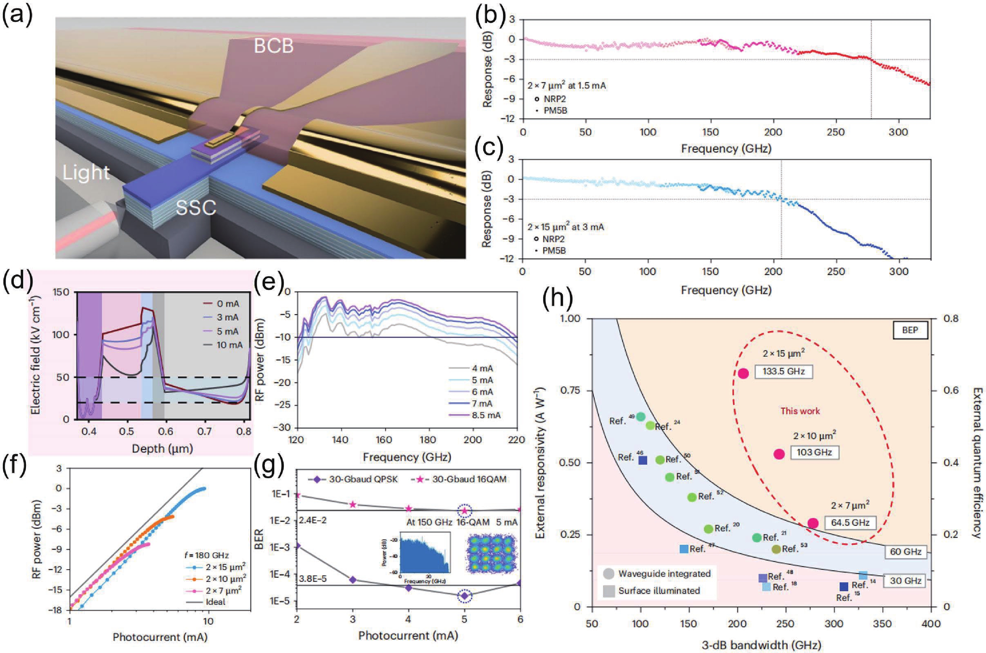
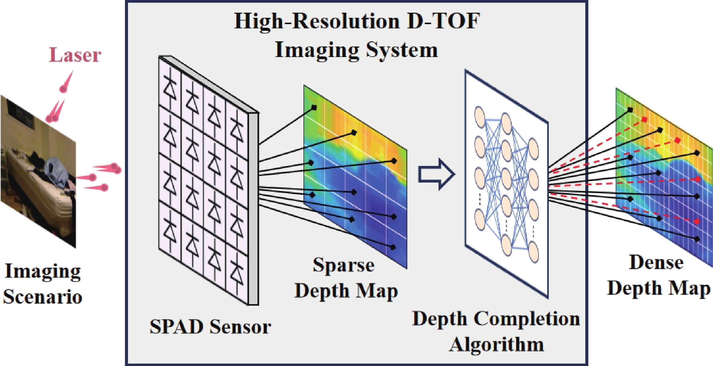
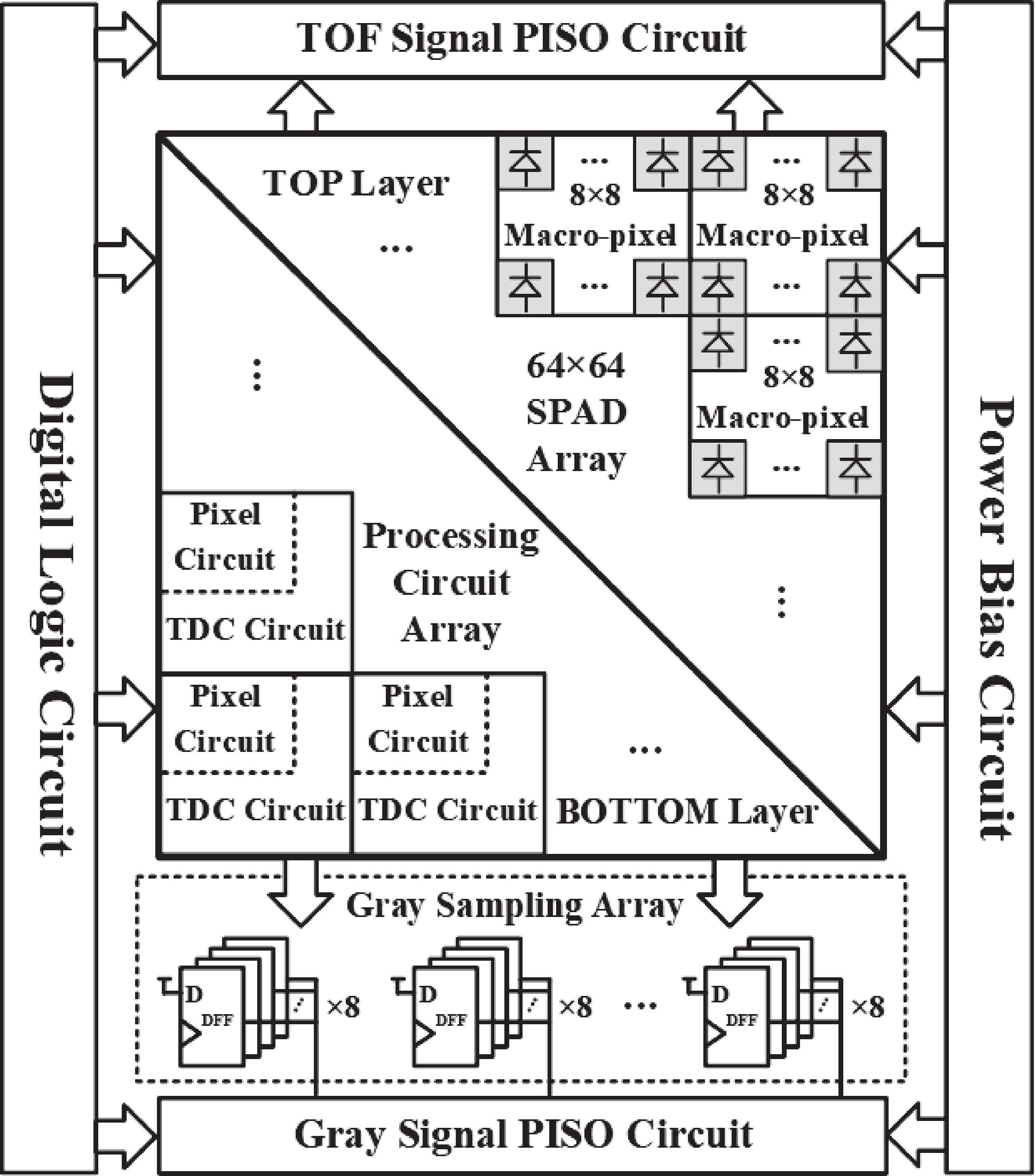
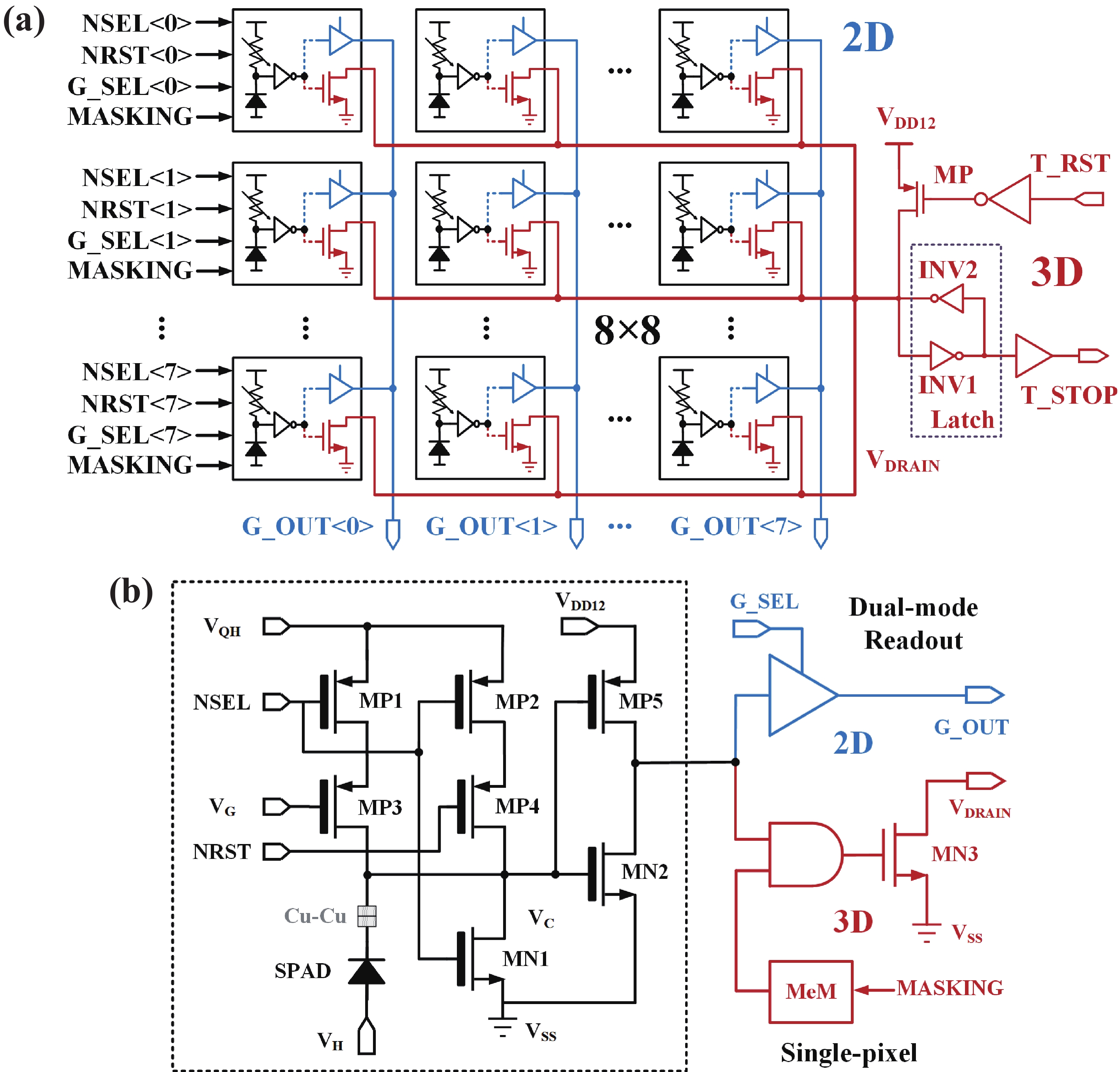
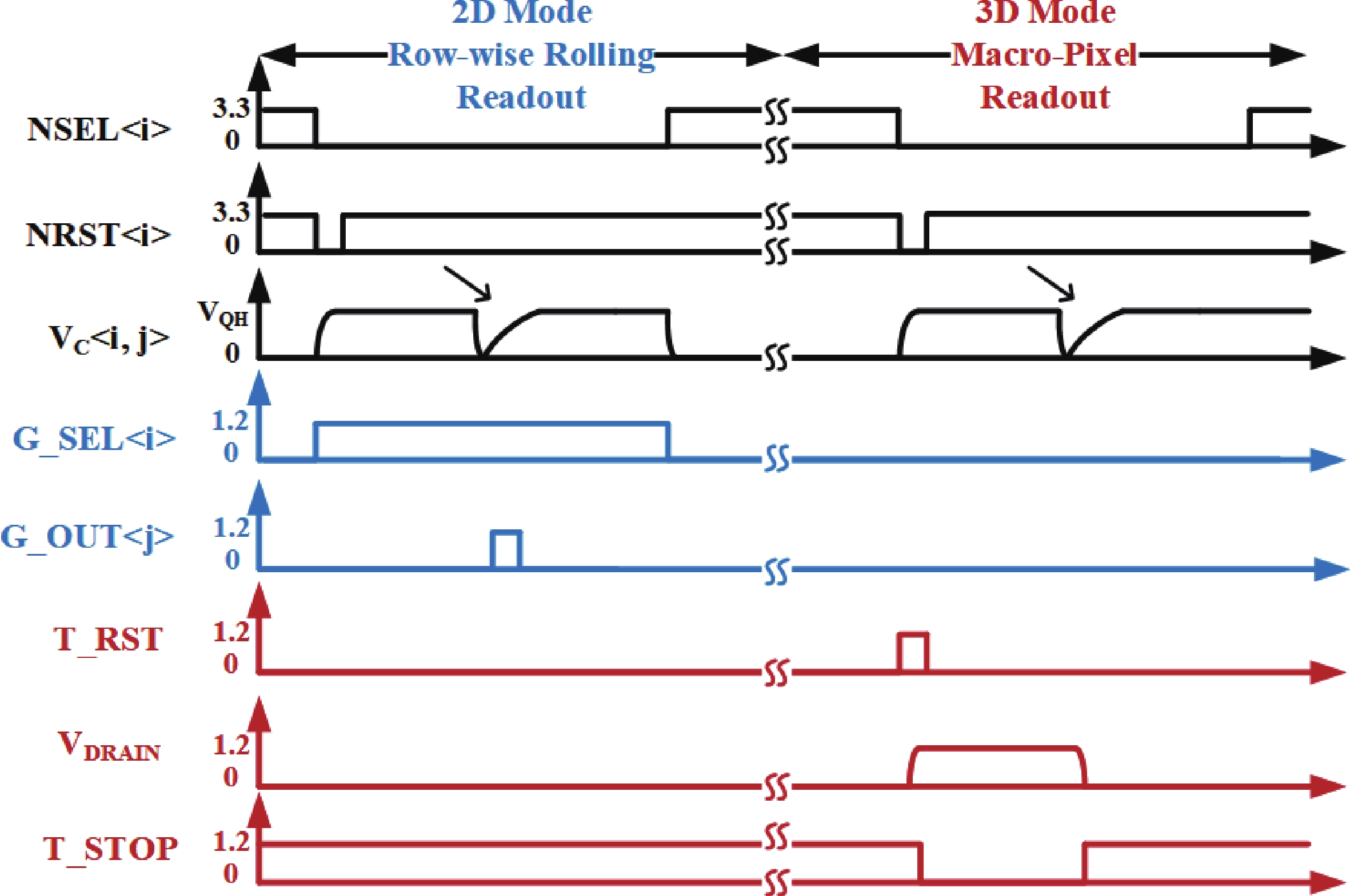
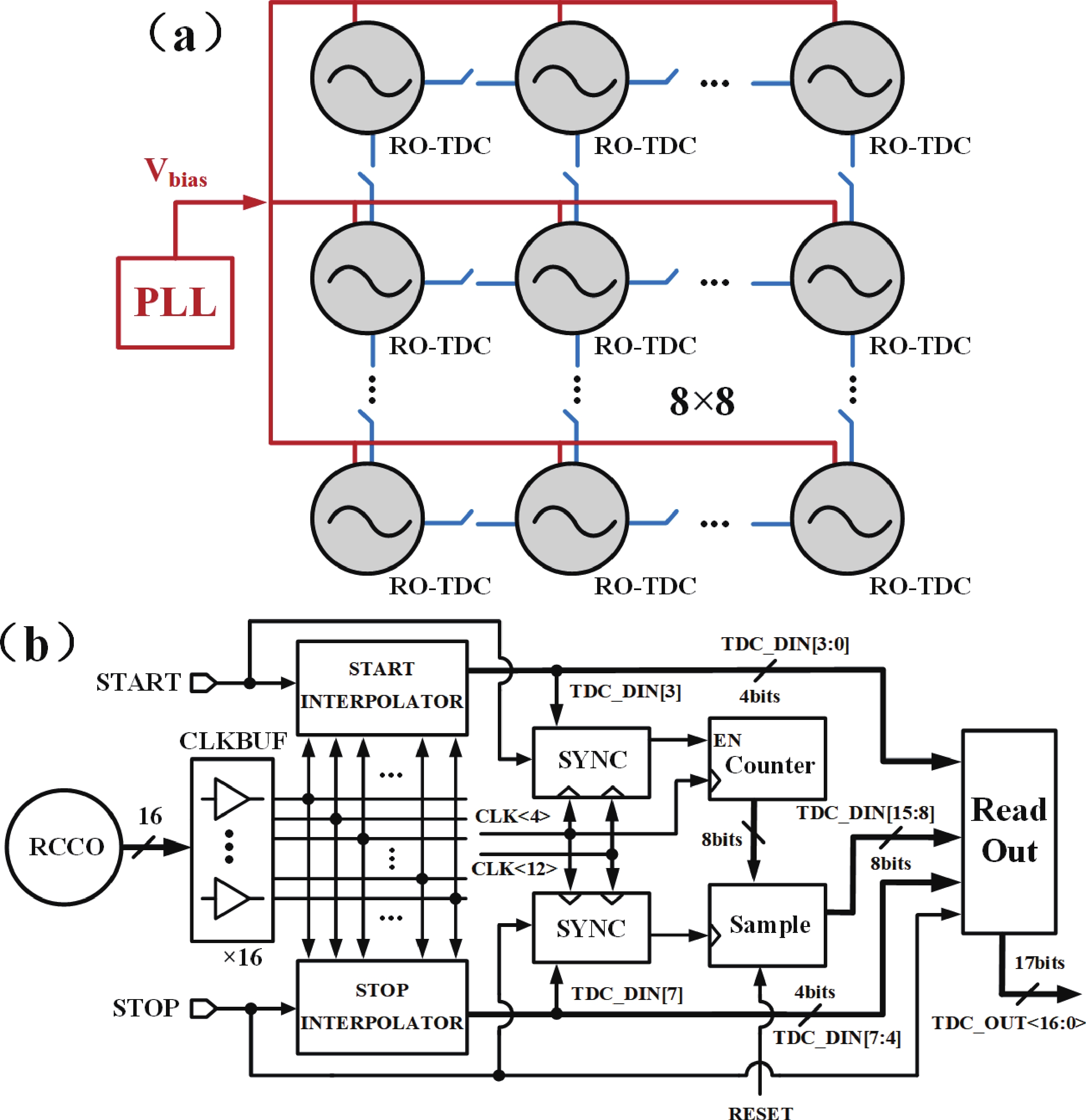
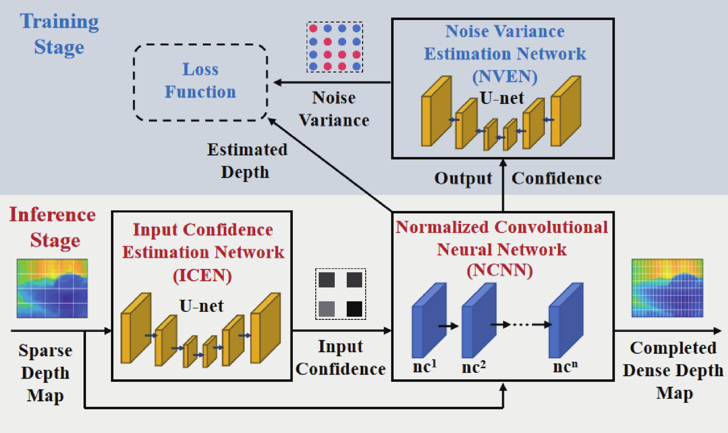
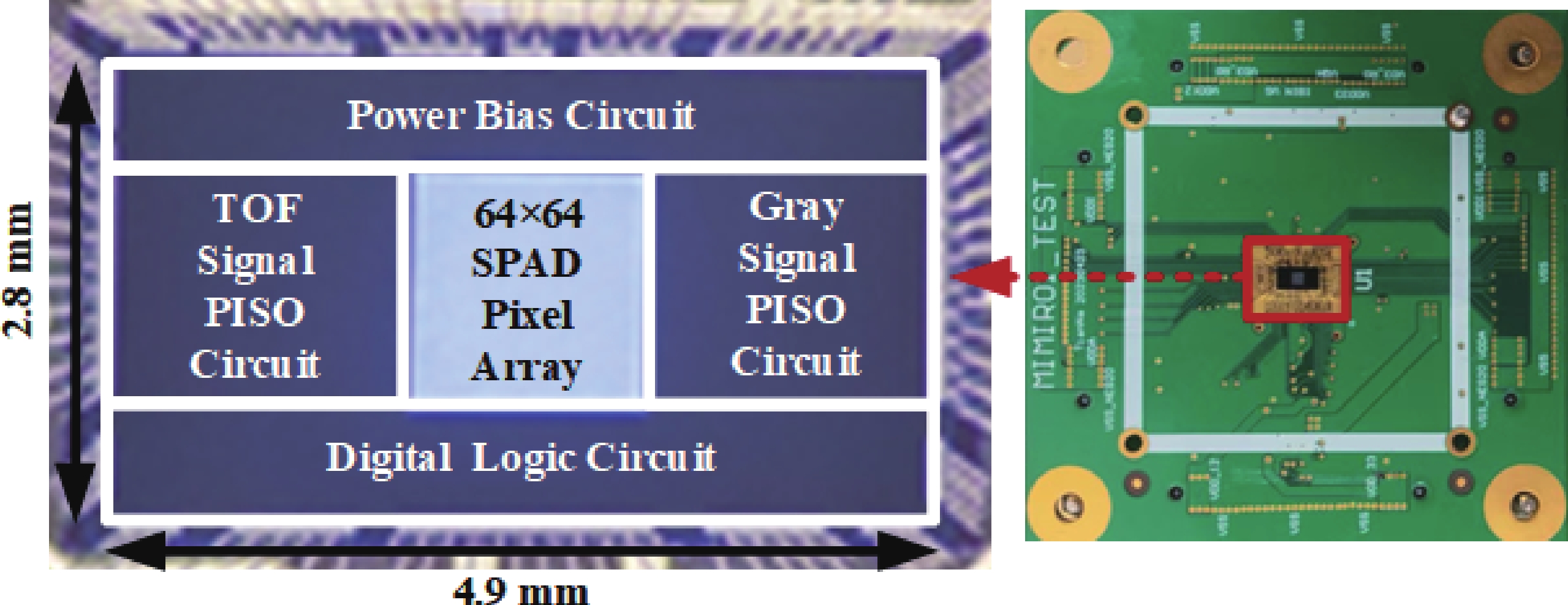
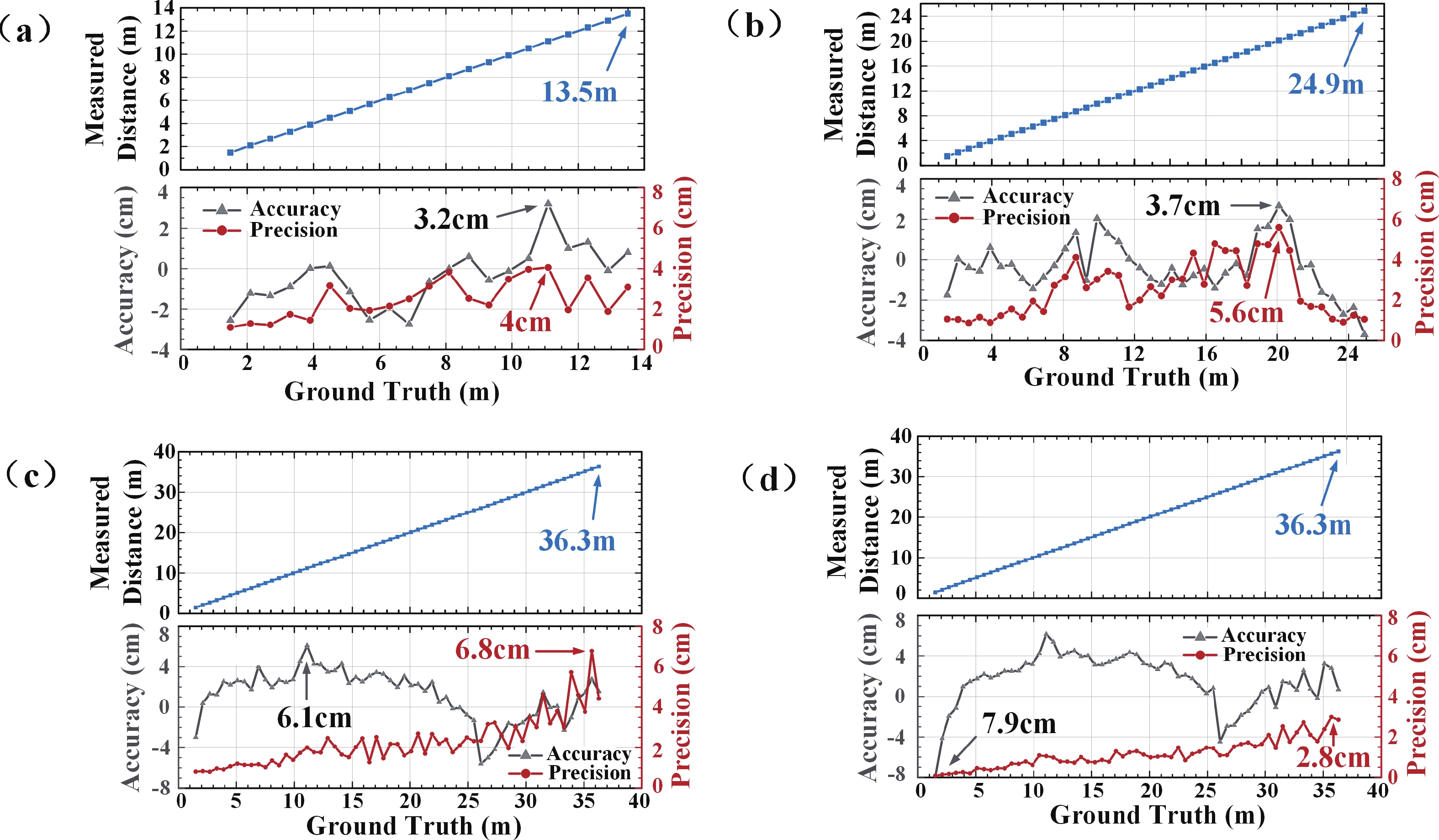
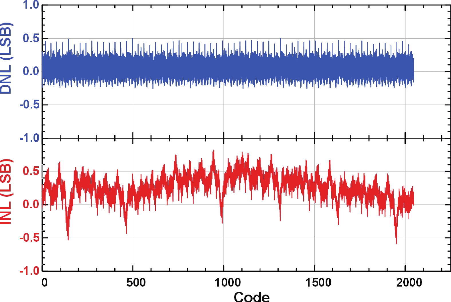
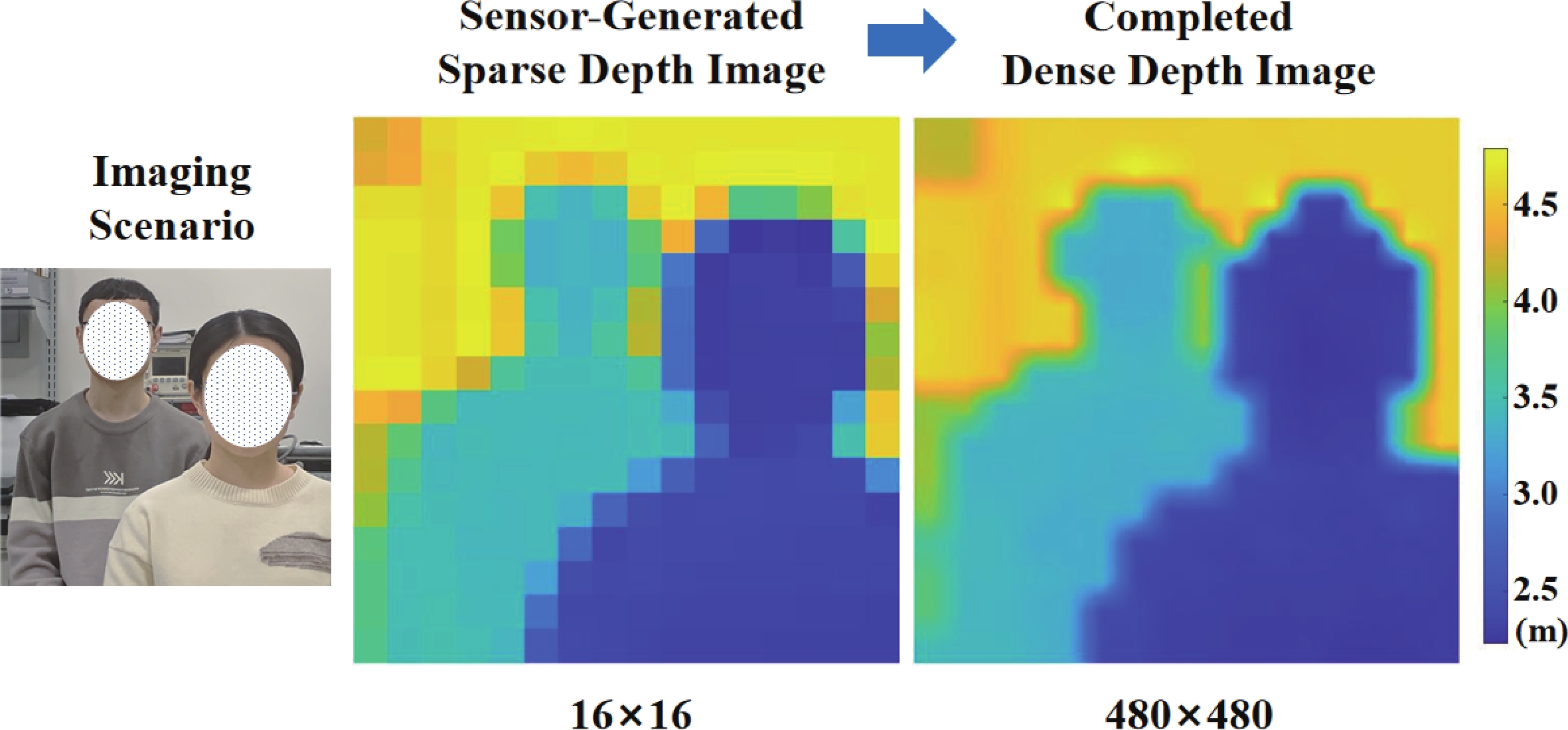
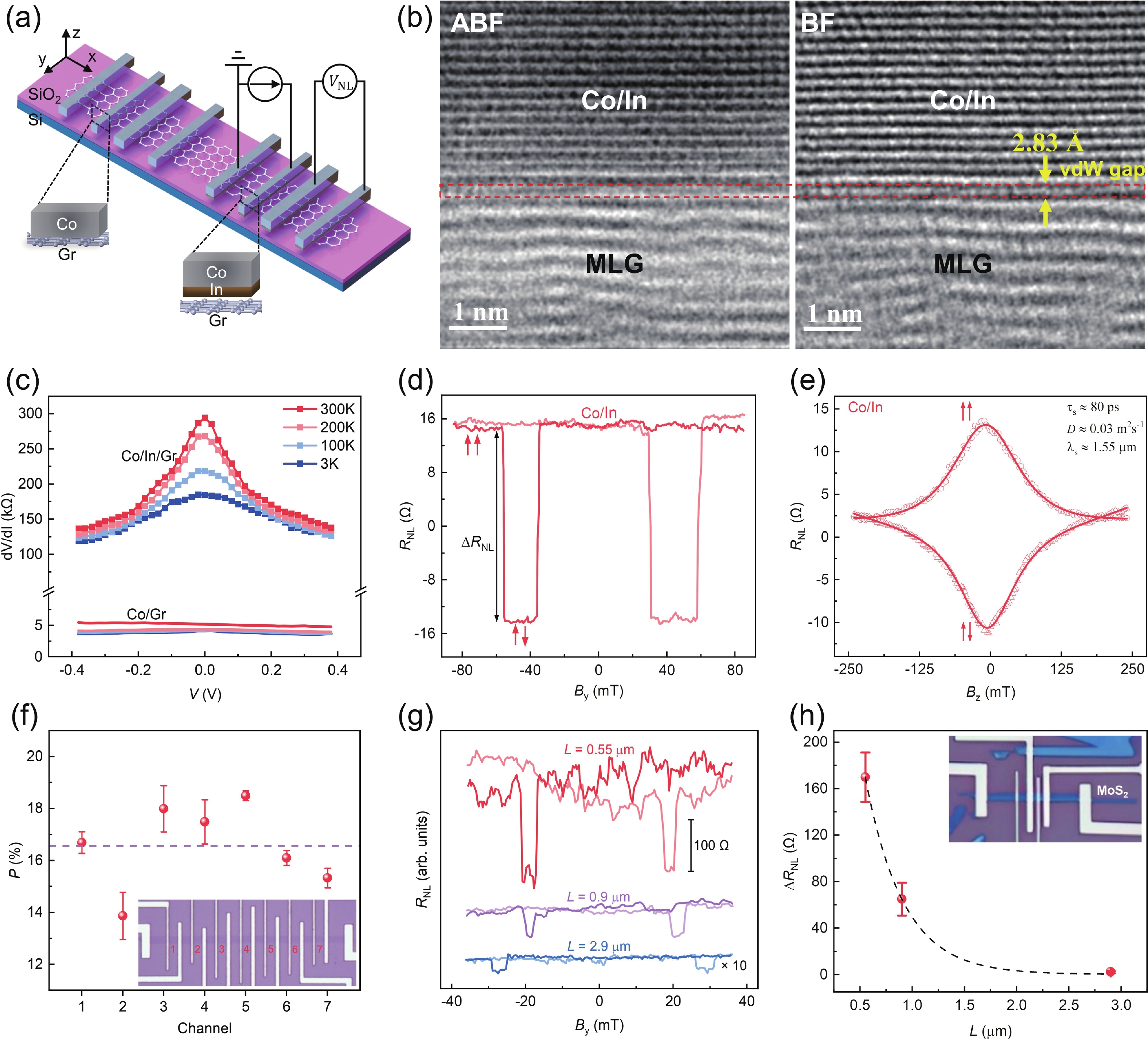
Single-photon avalanche diode (SPAD) image sensors are widely used in direct time-of-flight (D-TOF) imaging, but their ranging performance is often constrained by limited laser power. This article presents a SPAD-based D-TOF imaging system that combines a reconfigurable macro-pixel sensor architecture with a lightweight depth completion algorithm to achieve long-range depth imaging with enhanced spatial resolution under low optical power. The proposed sensor adopts a back-side illuminated (BSI) 3D-stacked architecture with programmable macro-pixels that enhance detection sensitivity and enable flexible sensitivity–resolution trade-offs. An injection-locked ring-oscillator-based time-to-digital converter (RO-TDC) array achieves a time resolution of 152.5 ps, enabling accurate TOF measurement at an optical power of 10 mW. To compensate for macro-pixel-induced resolution loss, a probabilistic normalized convolutional neural network (pNCNN) is employed for depth completion using sparse depth inputs only. Experimental results demonstrate that up to 30 × effective resolution enhancement of the system can be achieved via the depth completion algorithm without changing the physical resolution of the sensor. Additionally, the proposed system achieves a maximum ranging distance of 90 m and a range-to-power figure-of-merit (FOM) of 9 m/mW, which validates the effectiveness of the system.
Just Accepted manuscripts are peer-reviewed and accepted for publication. They are posted online prior to technical editing formatting for publication and author proofing.
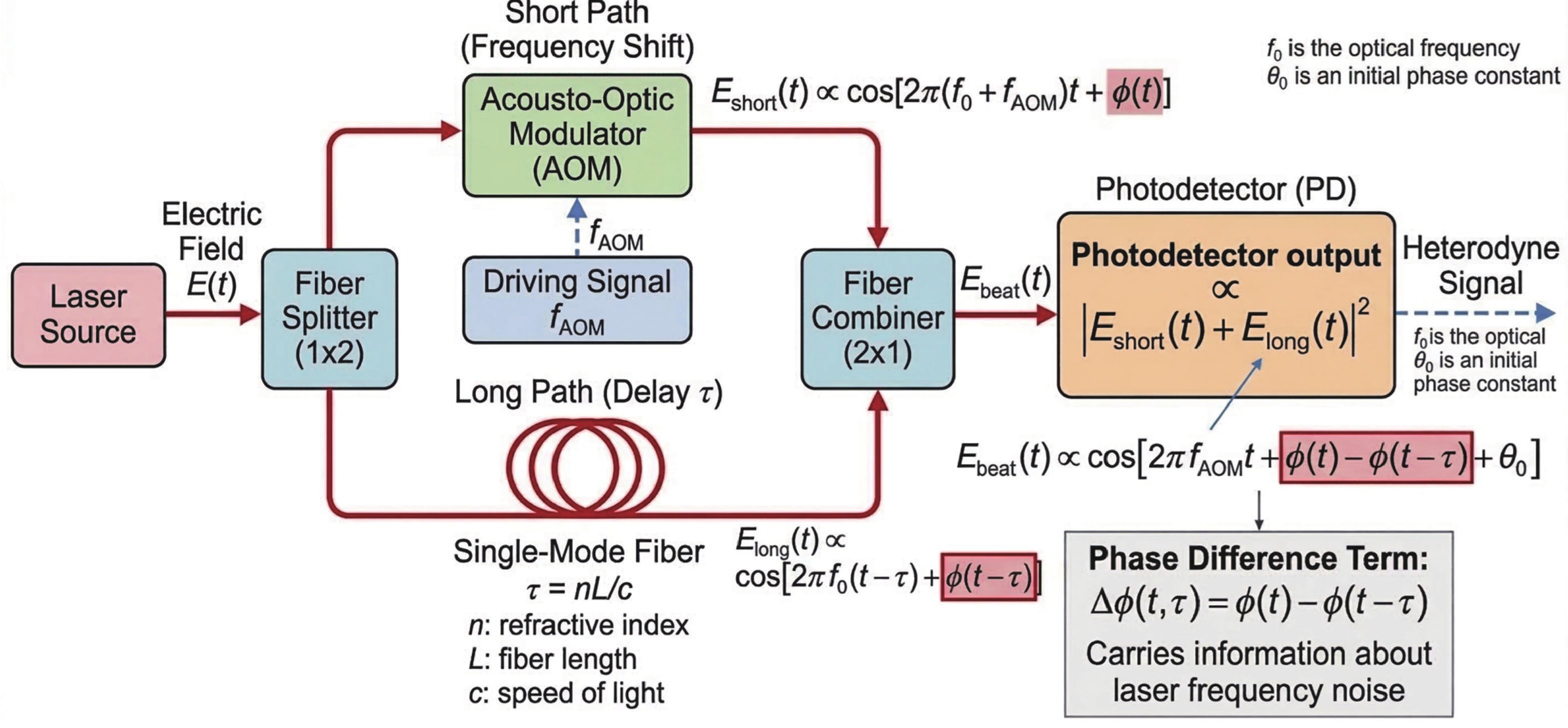
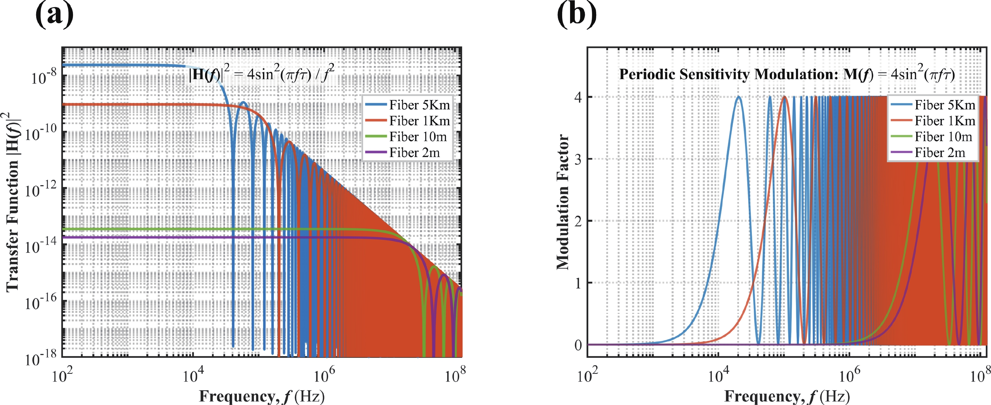
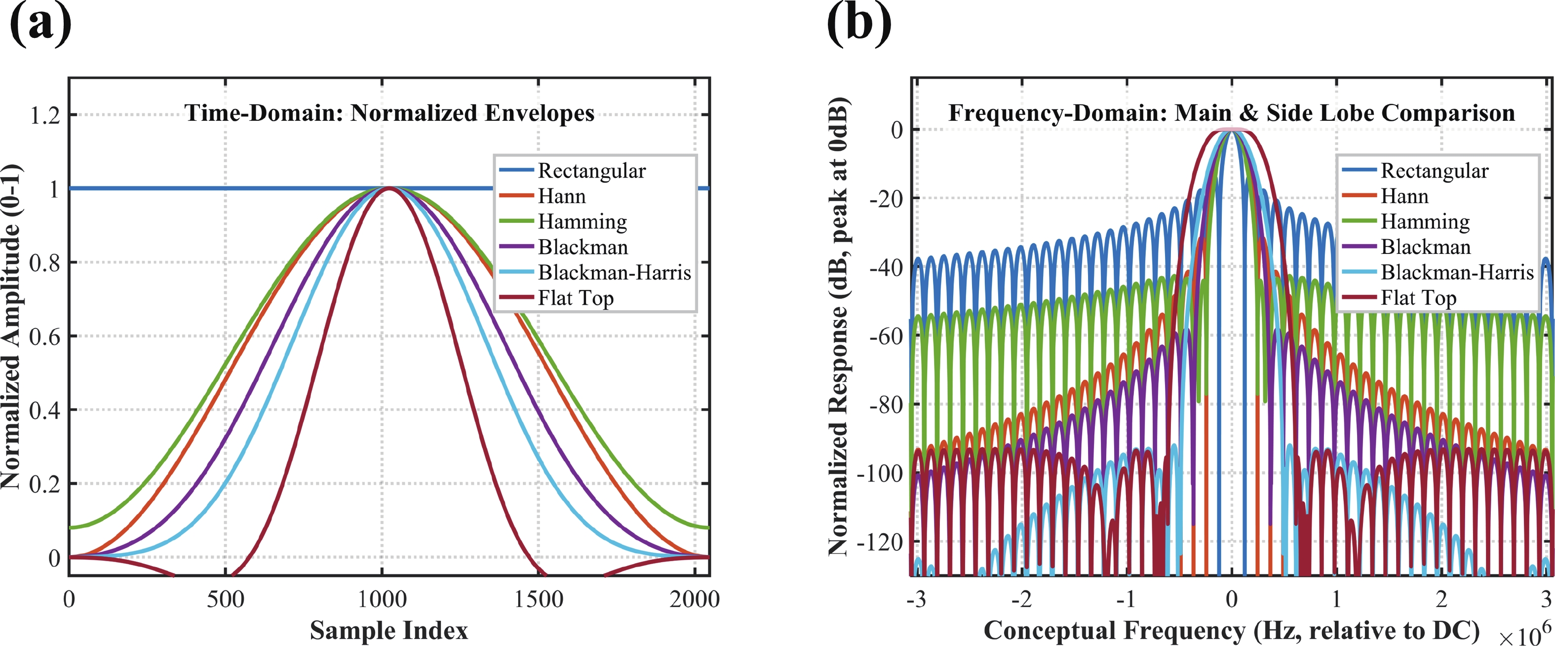
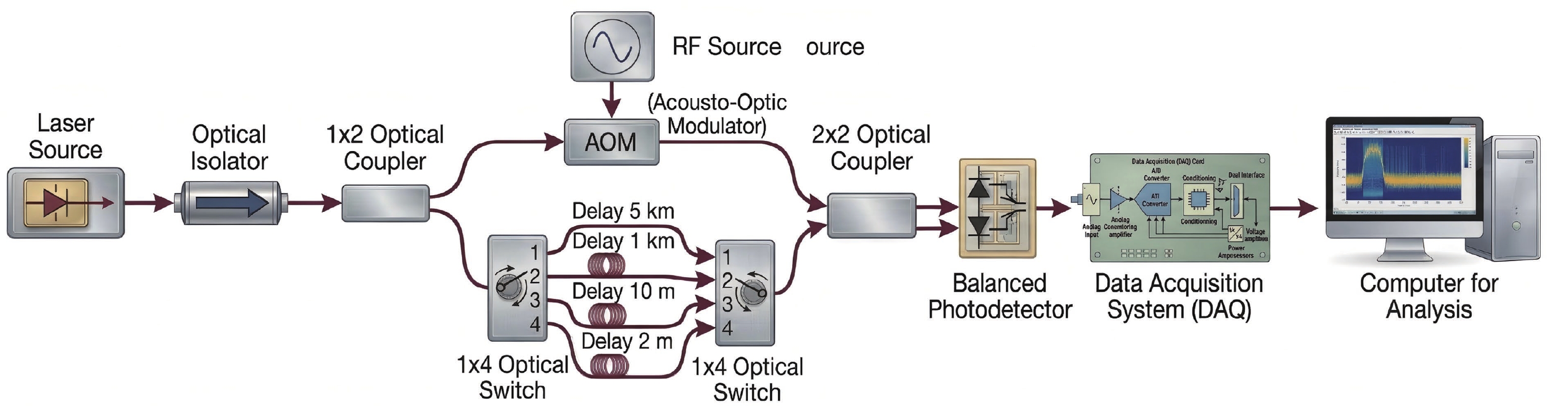
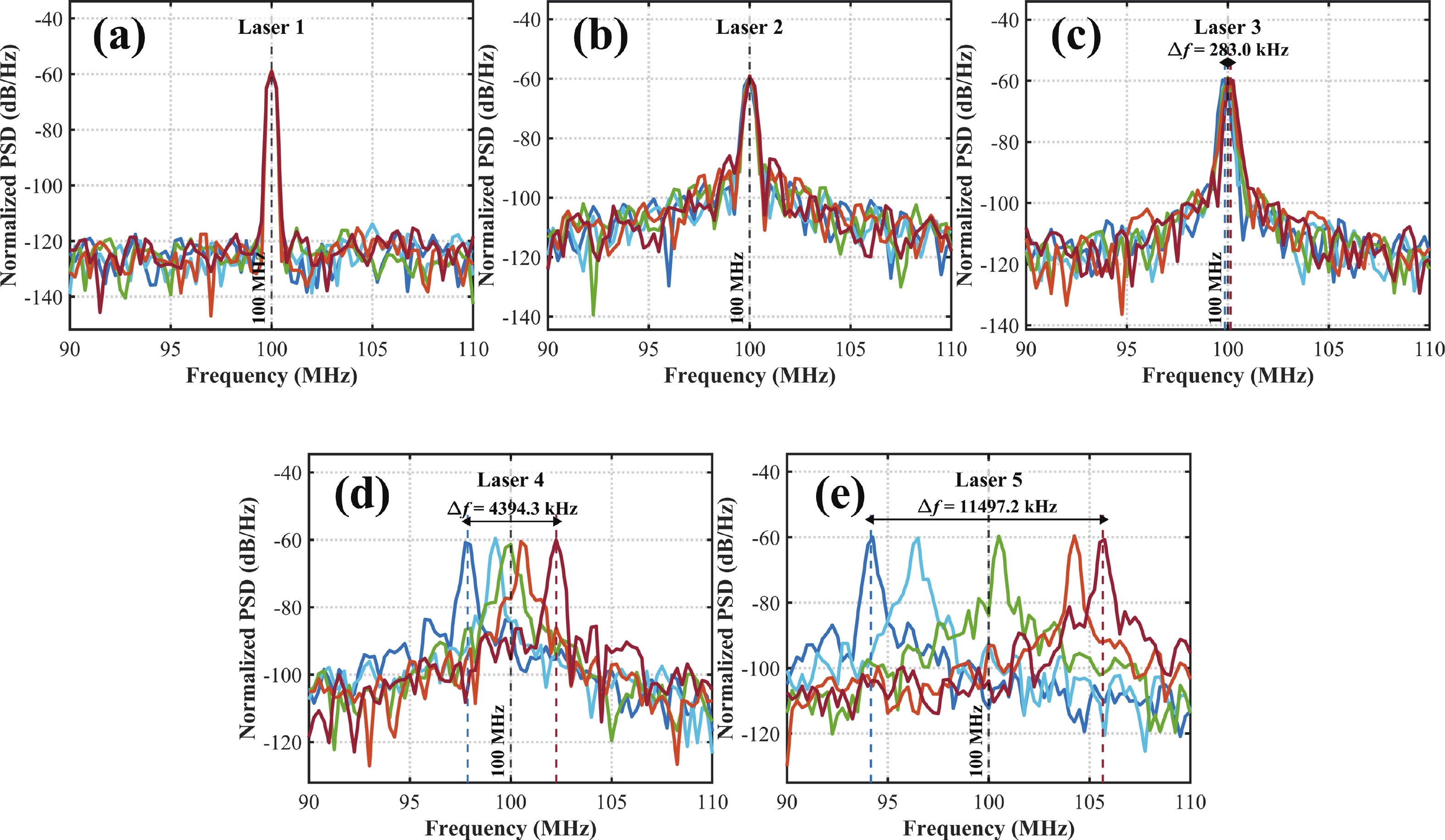
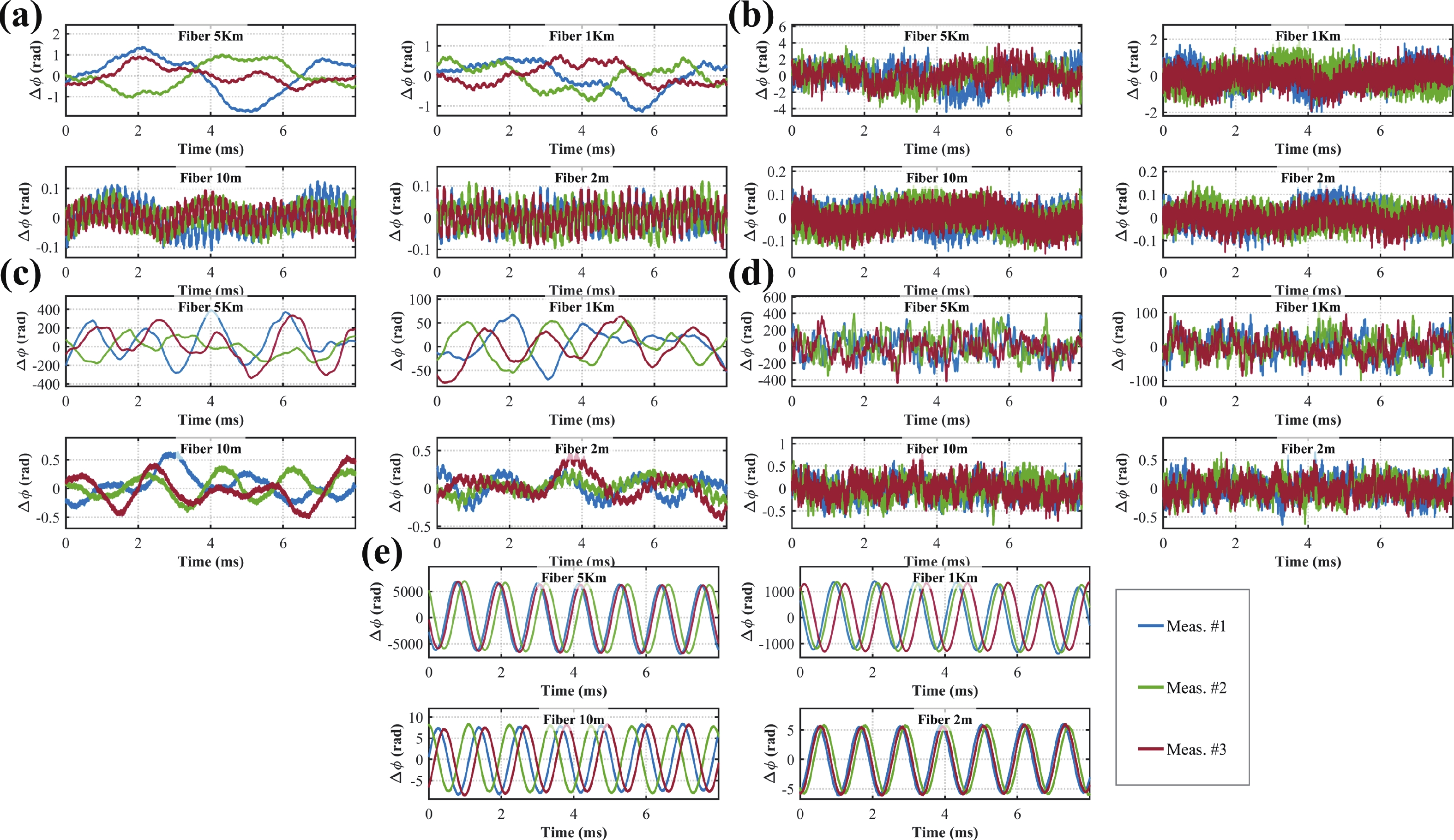
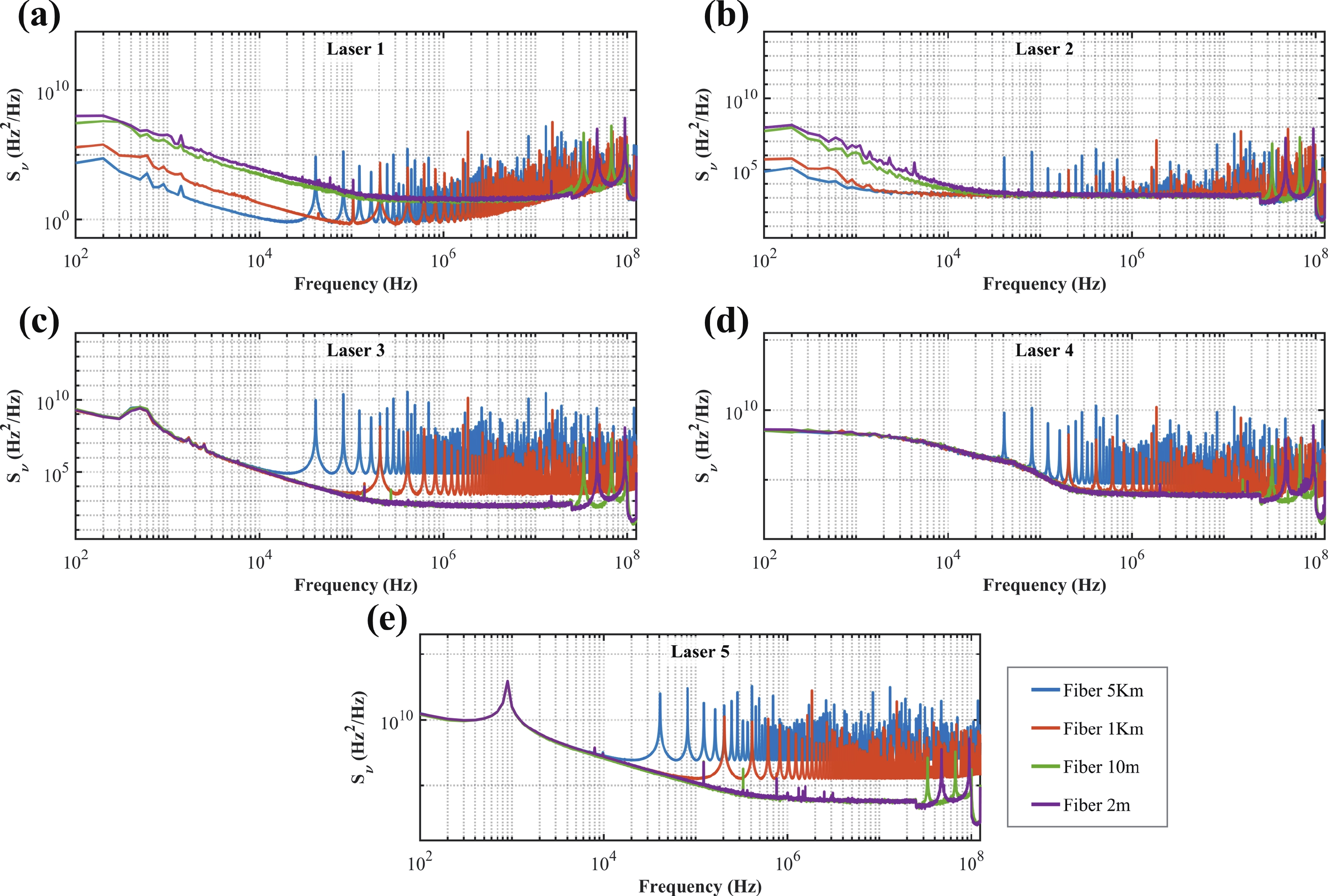
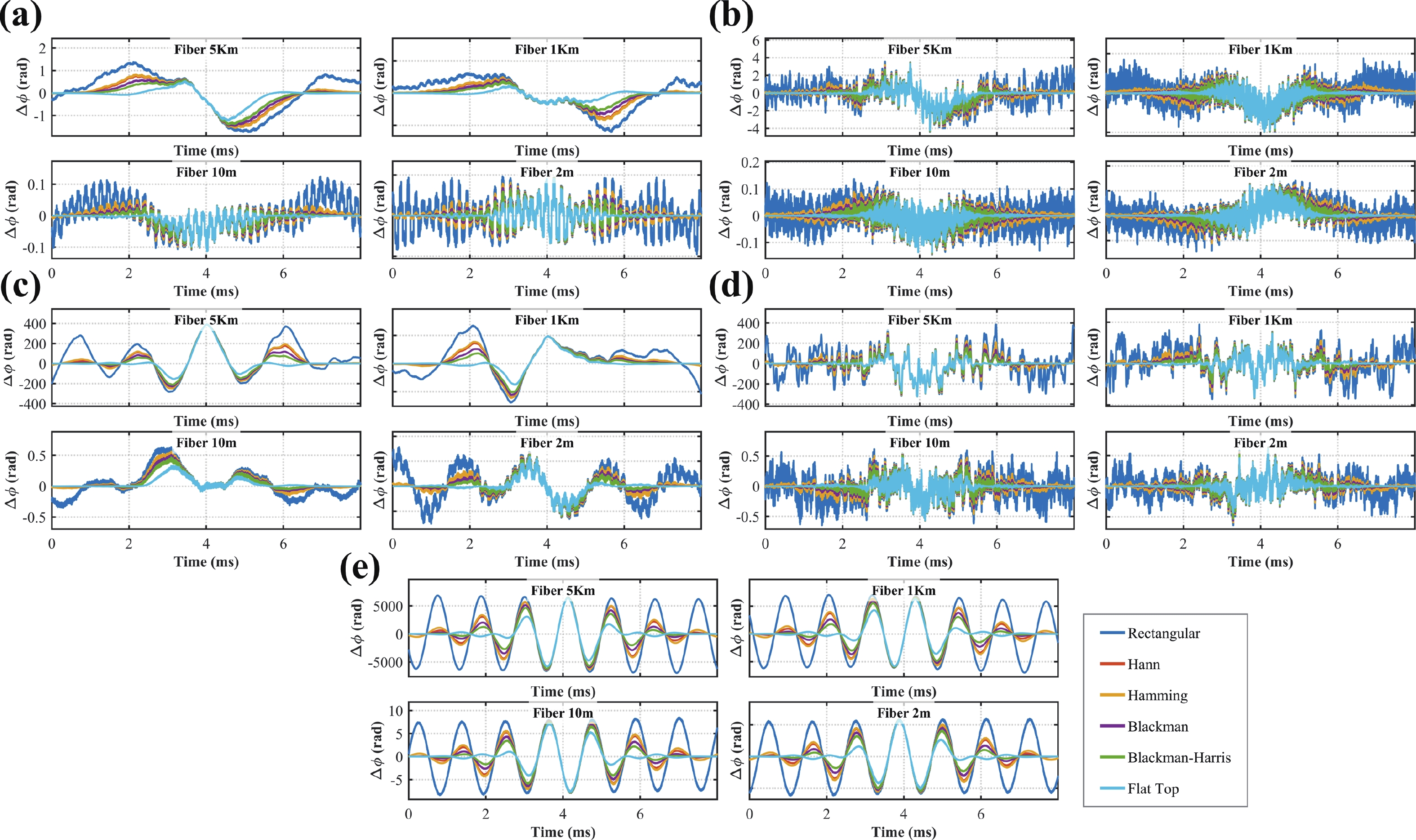
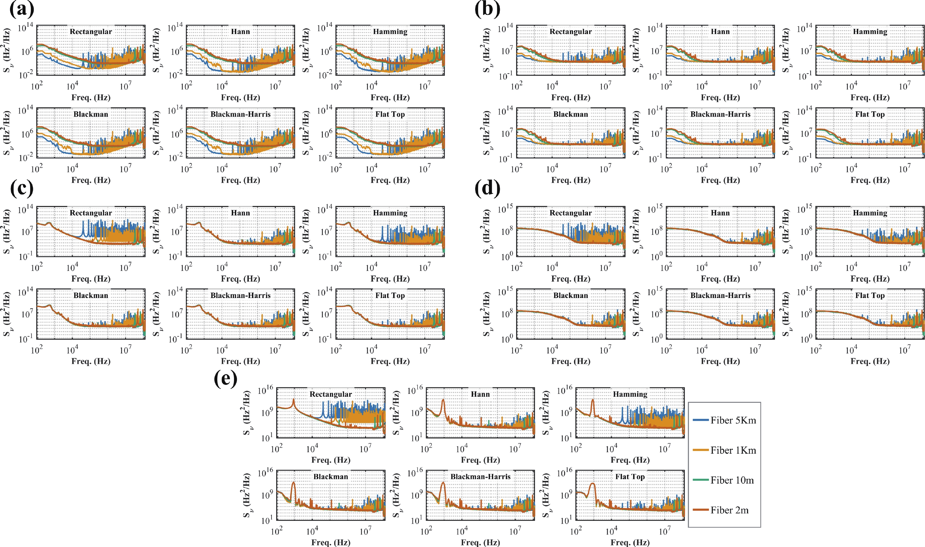
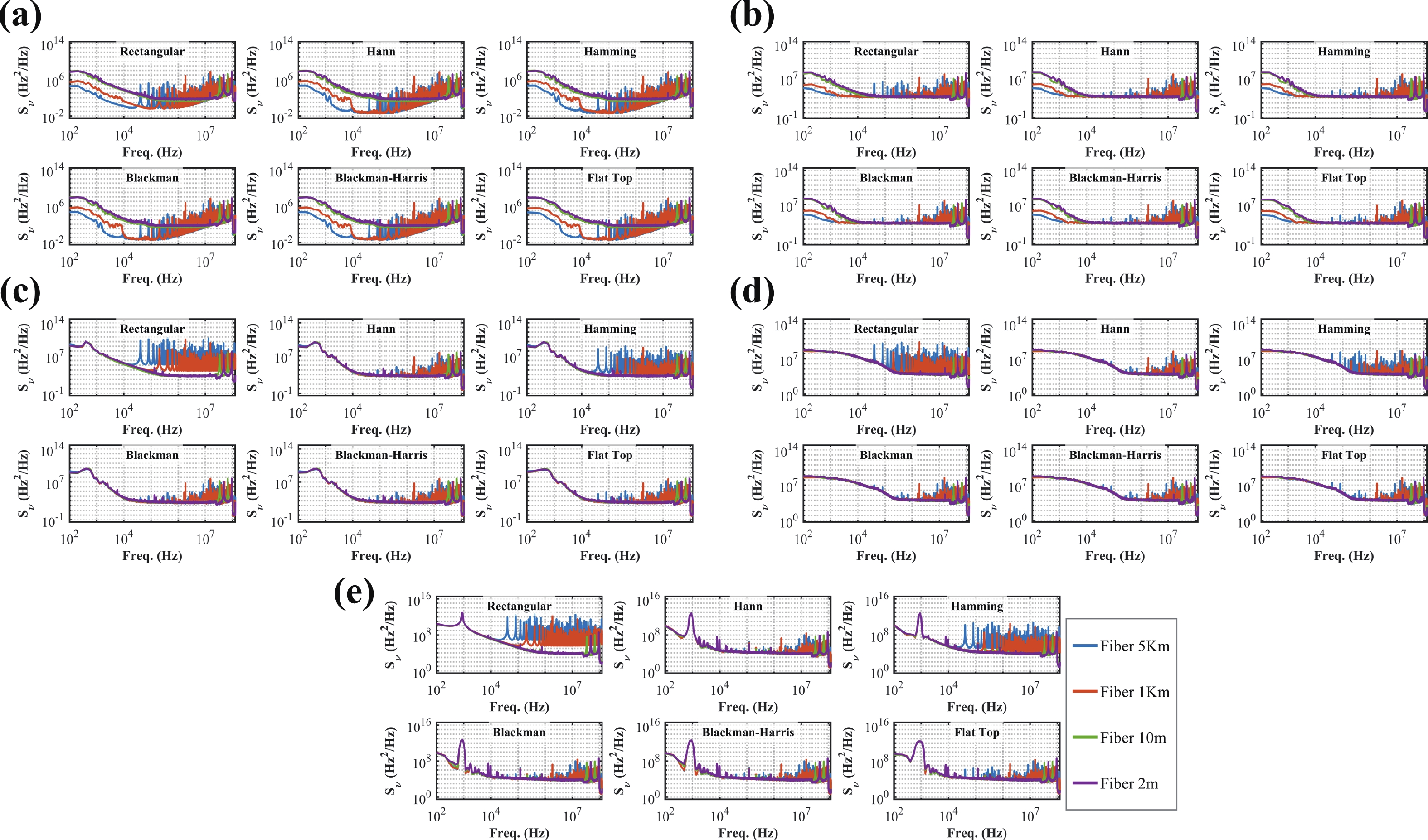
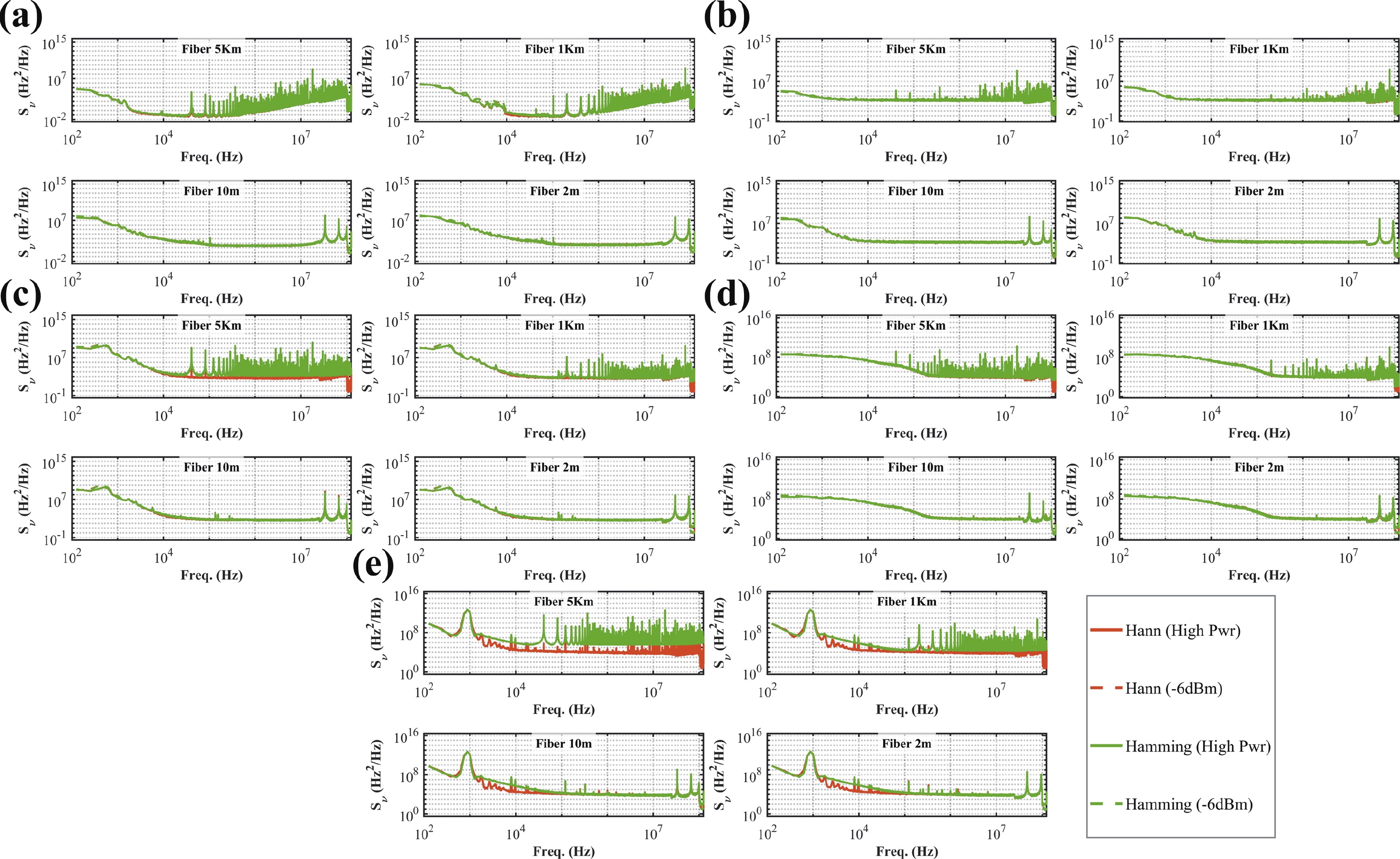
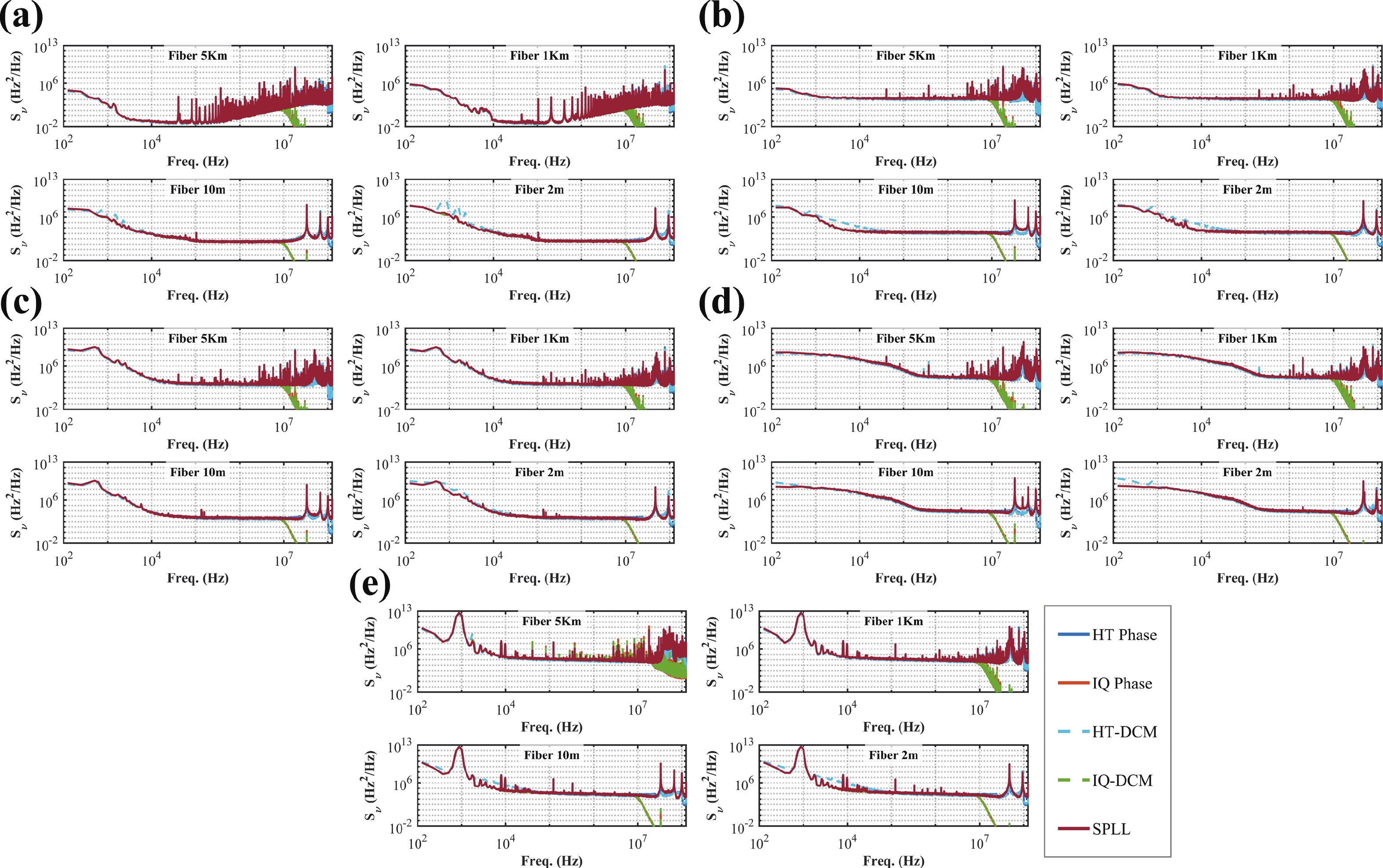
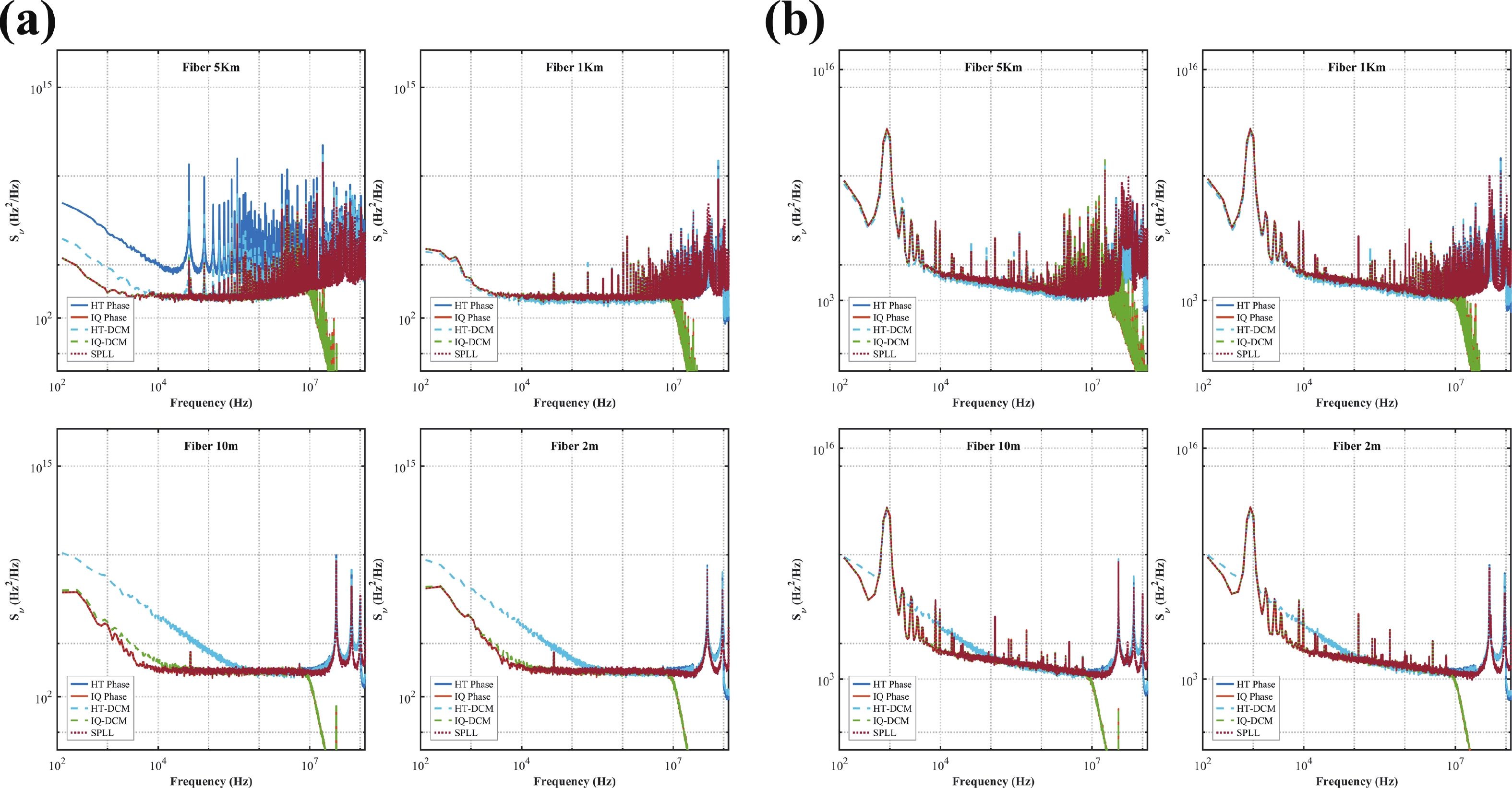
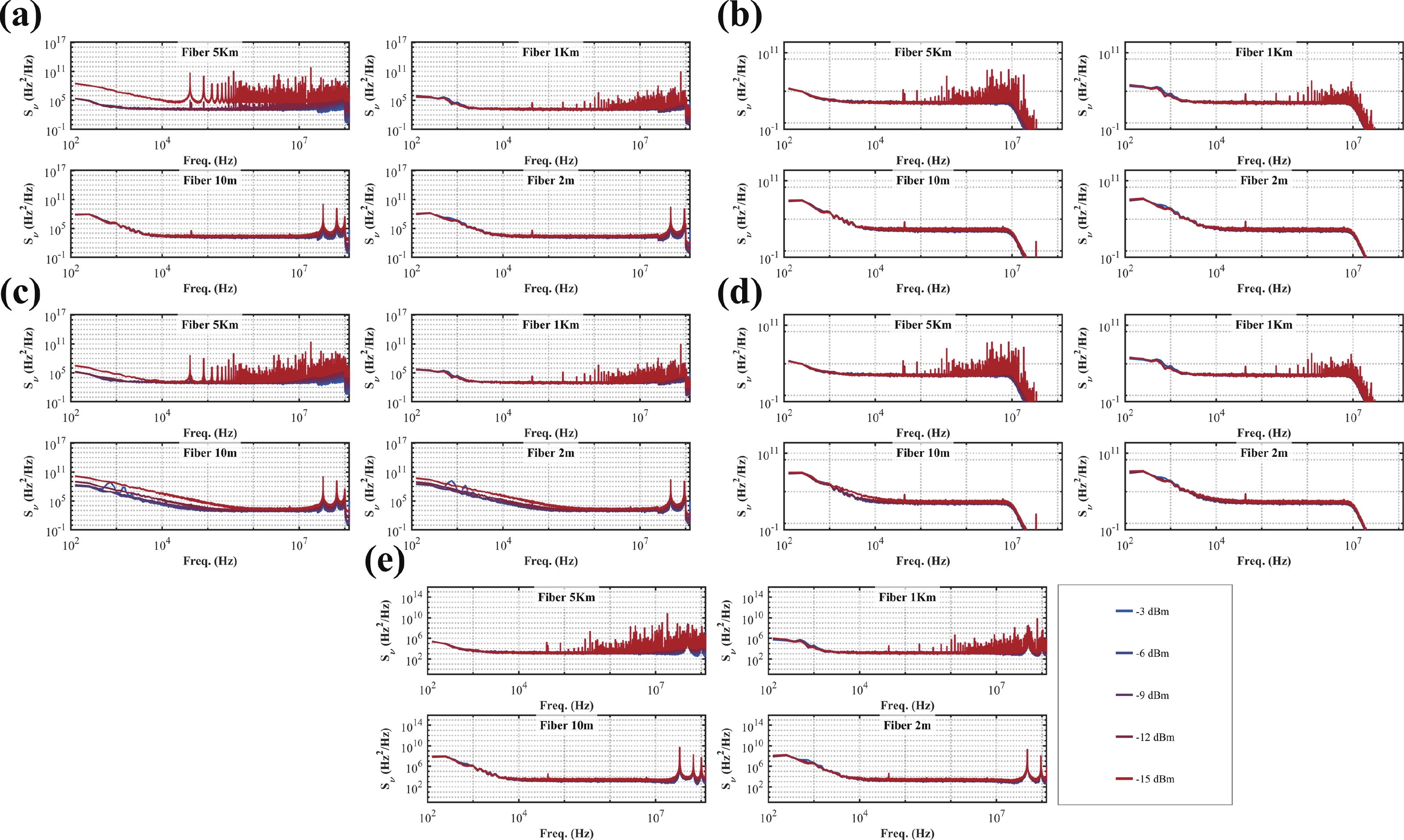
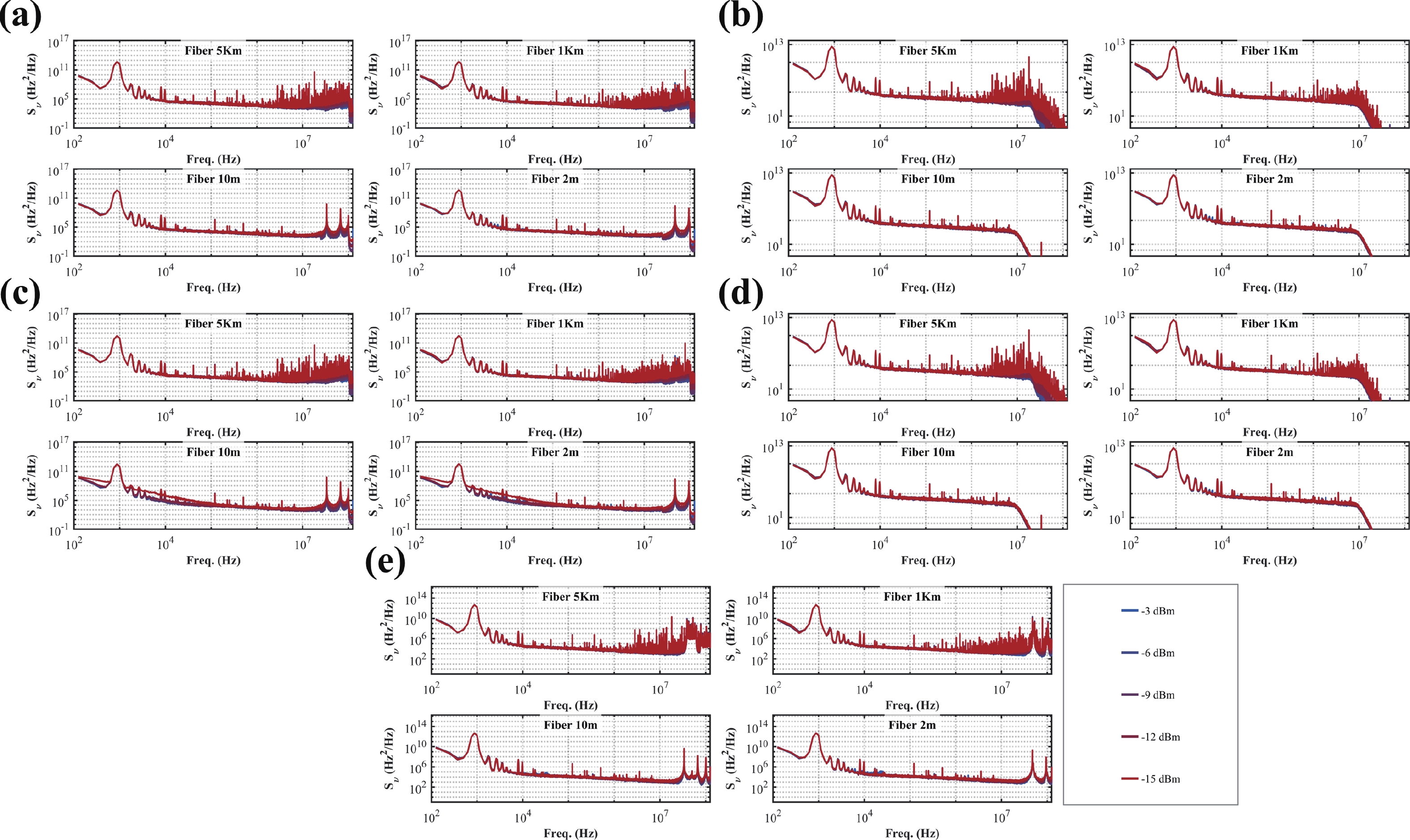
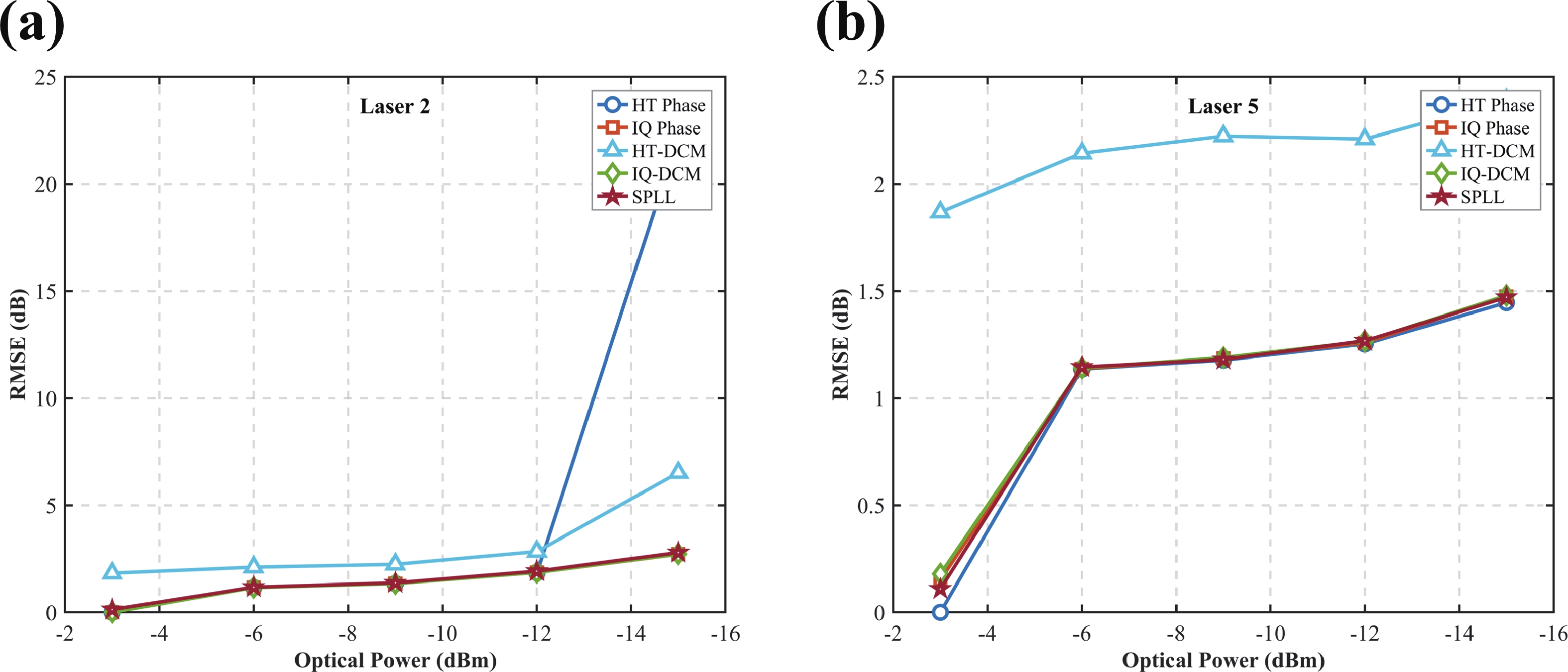
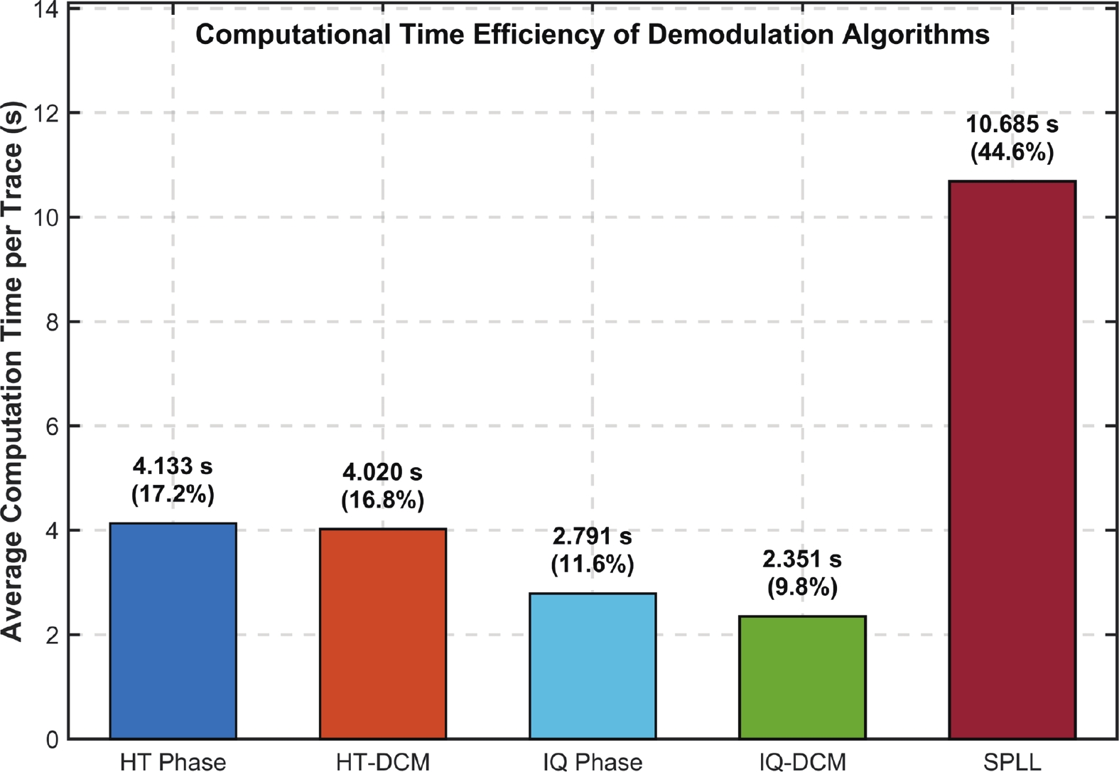
Systematic optimization of the delayed self-heterodyne method for laser frequency noise characterization is investigated across an extensive linewidth range (100 Hz to 10 MHz). By evaluating various fiber lengths, window functions, and five demodulation algorithms, we identify a critical trade-off: long fibers enhance sensitivity for narrow-linewidth lasers but exacerbate spectral leakage in broad-linewidth sources. Our findings demonstrate that Hanning and Blackman windows effectively suppress this leakage, ensuring measurement consistency across different delay lengths. Among the evaluated algorithms, the Hilbert transform offers the superior balance of high-frequency accuracy and computational efficiency. Validated under low-power conditions, this optimized framework provides a robust and power-independent methodology for precise FN analysis, offering significant guidance for high-performance laser development.


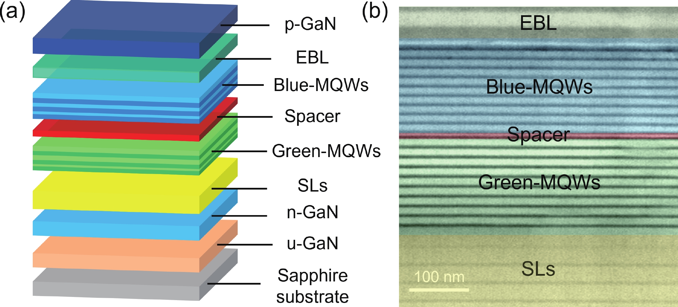
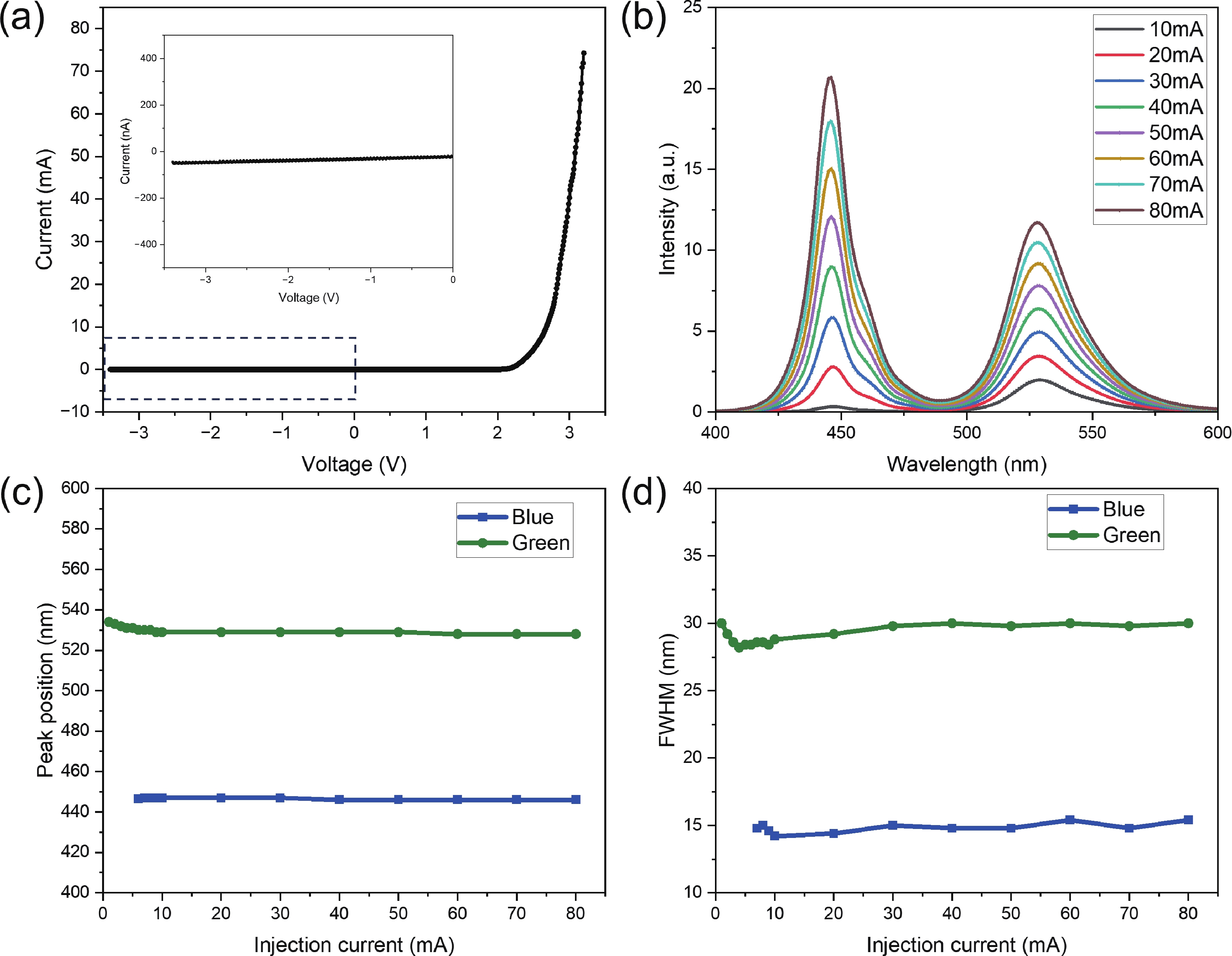
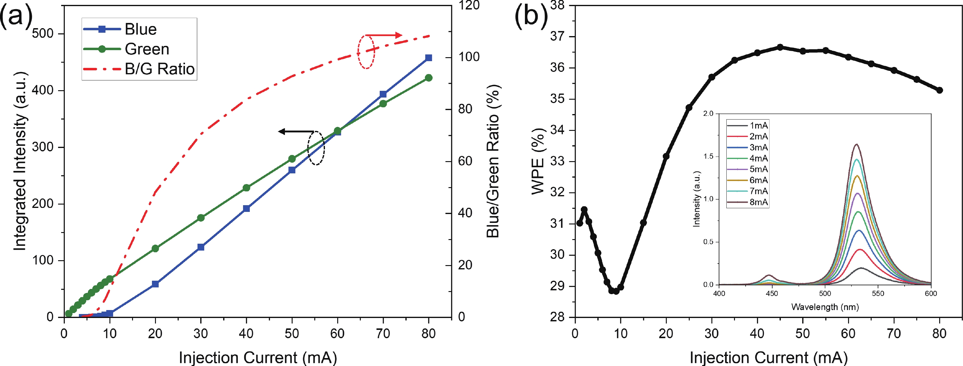
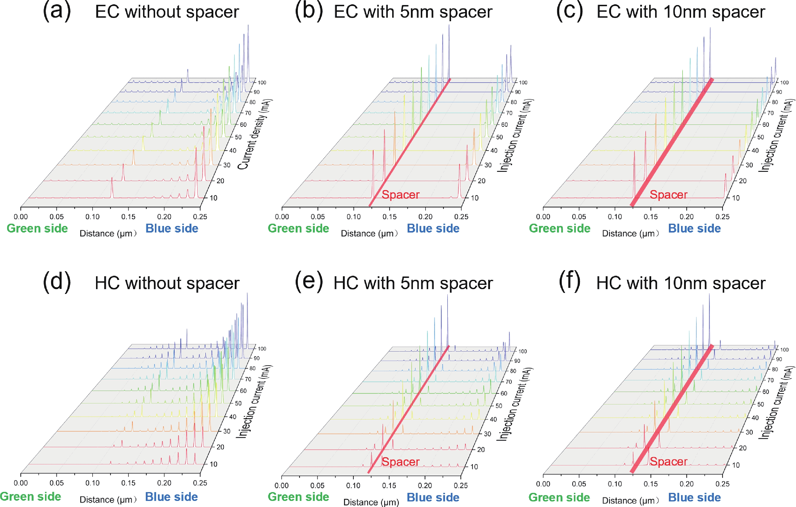
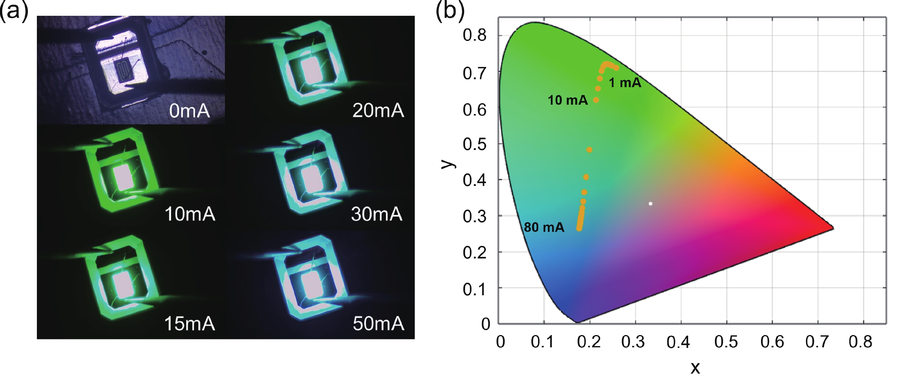
III-nitride semiconductors with continuously tunable bandgaps are promising for white light emission and full-color displays. The mainstream RGB LED integration approach suffers from low long-wavelength efficiency and complex packaging. Herein, we demonstrate a novel single-chip dual-wavelength LED structure, which integrates blue (upper) and green (bottom) multiple quantum wells (MQWs) separated by a GaN intermediate spacer layer. The device exhibits two distinct emission peaks at 446 and 528 nm, with excellent luminescence stability. We investigate the role of the spacer layer and reveal its critical effect on the carrier distribution and radiative recombination behavior. The maximum wall-plug efficiency (WPE) of the device reaches approximately 36.7%, and its abnormal droop curve indicates a transition of the green emission mechanism from electroluminescence (EL) to photoluminescence (PL). By tuning the injection current, the dual-wavelength LED achieves a continuous color transition from green to blue, which corresponds to chromaticity coordinates ranging from (0.2584, 0.7098) to (0.1771, 0.2649) in the CIE 1931 chromaticity diagram. This work provides a feasible and flexible strategy for emission color modulation, and also lays a foundation for the development of high-performance solid-state lighting devices.


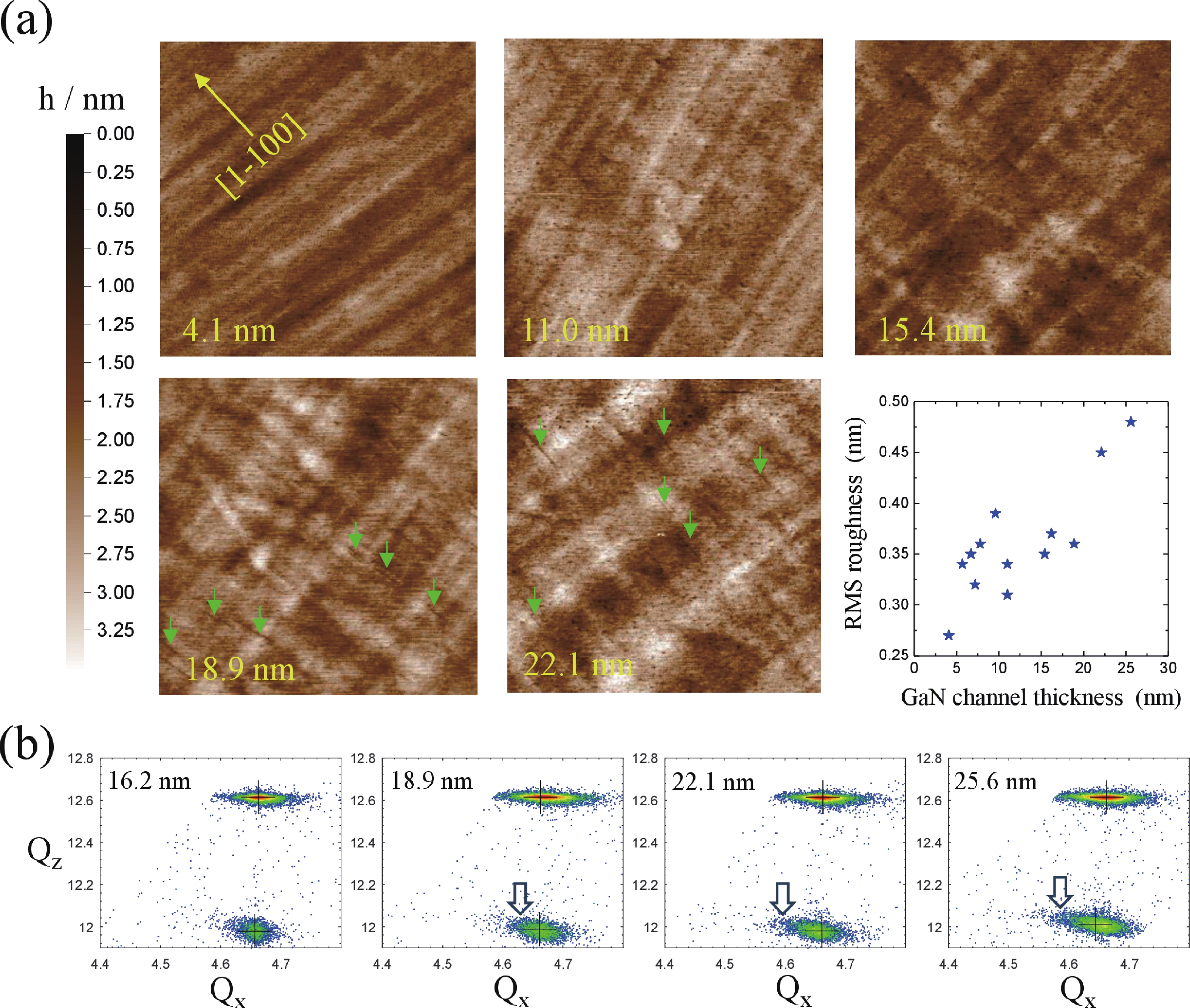
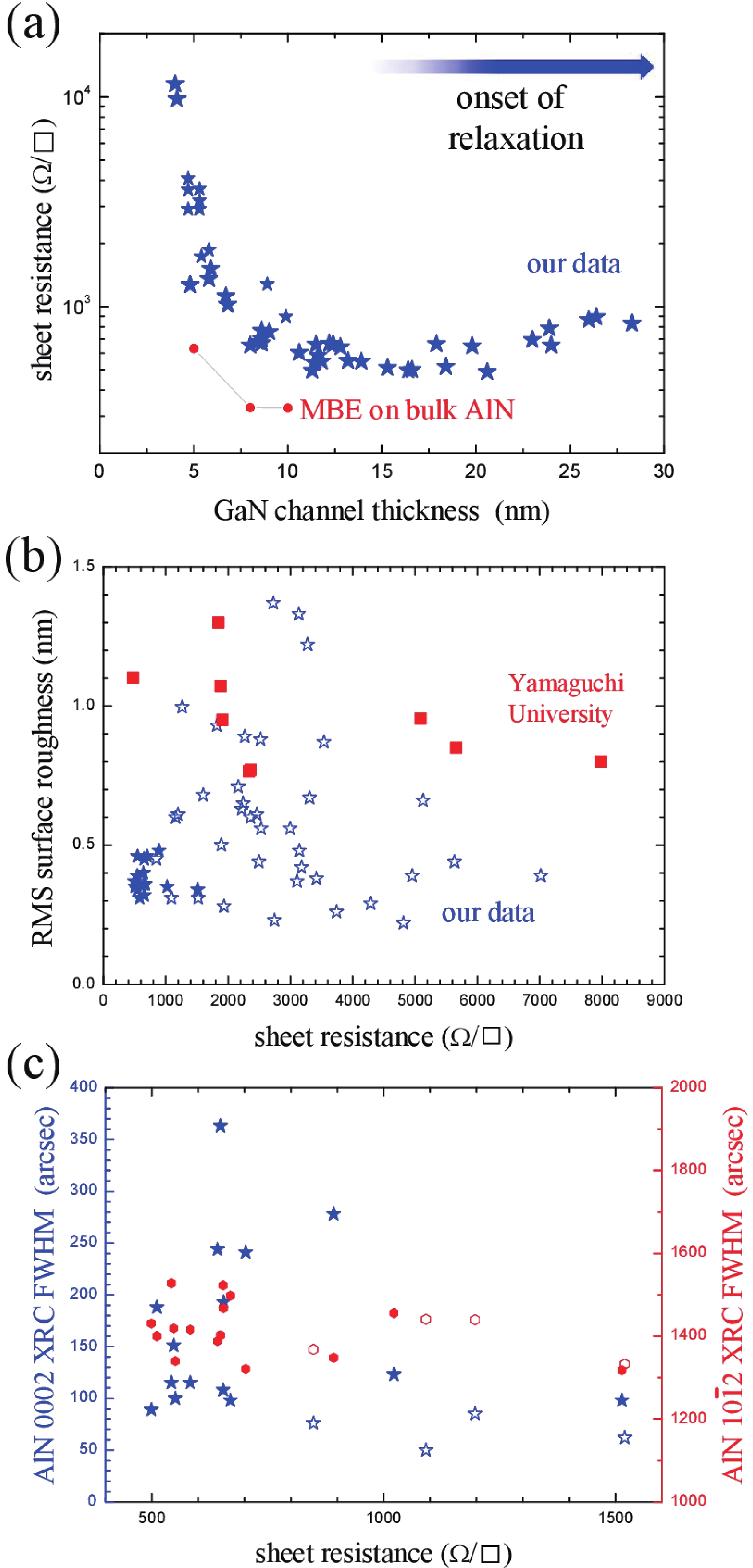
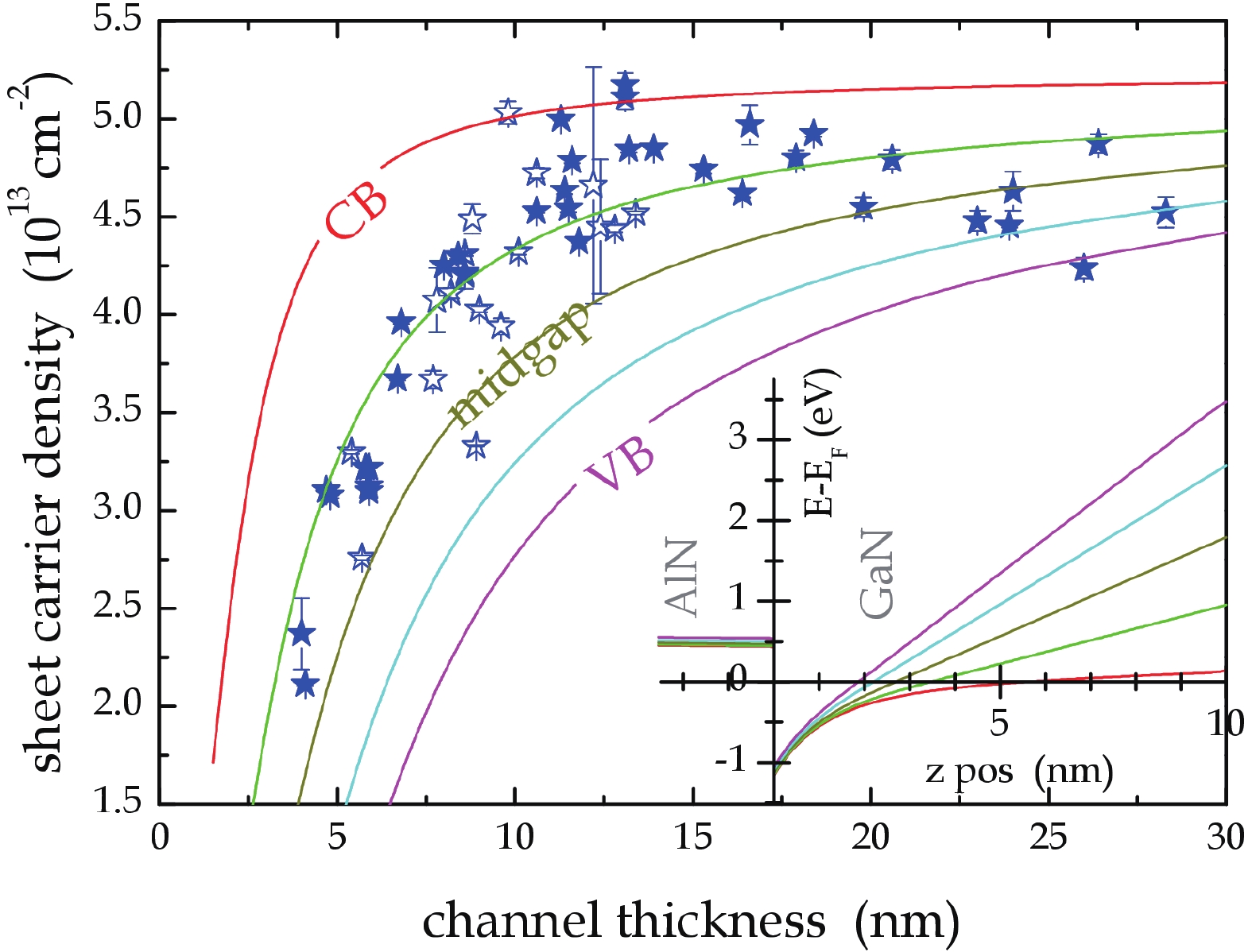
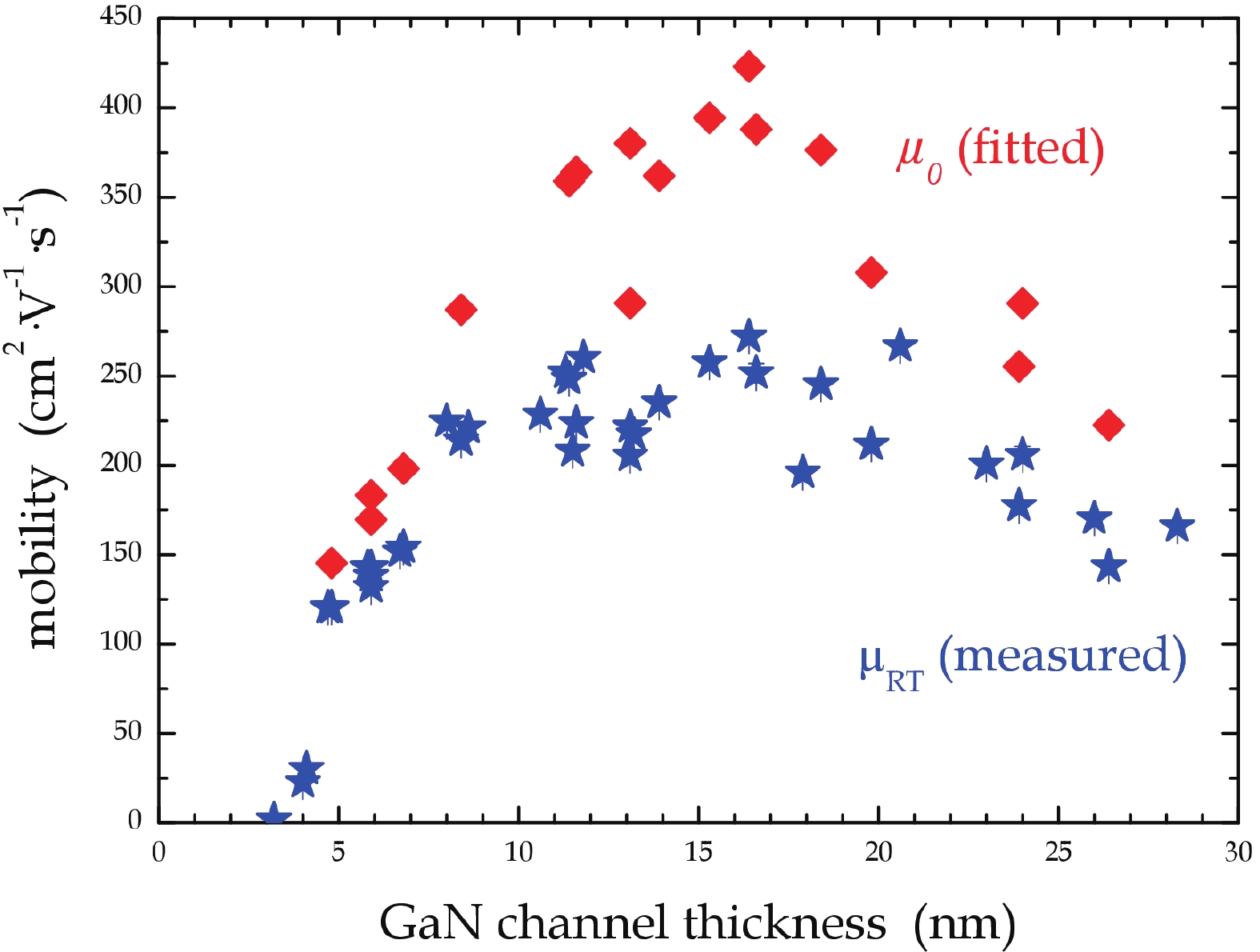
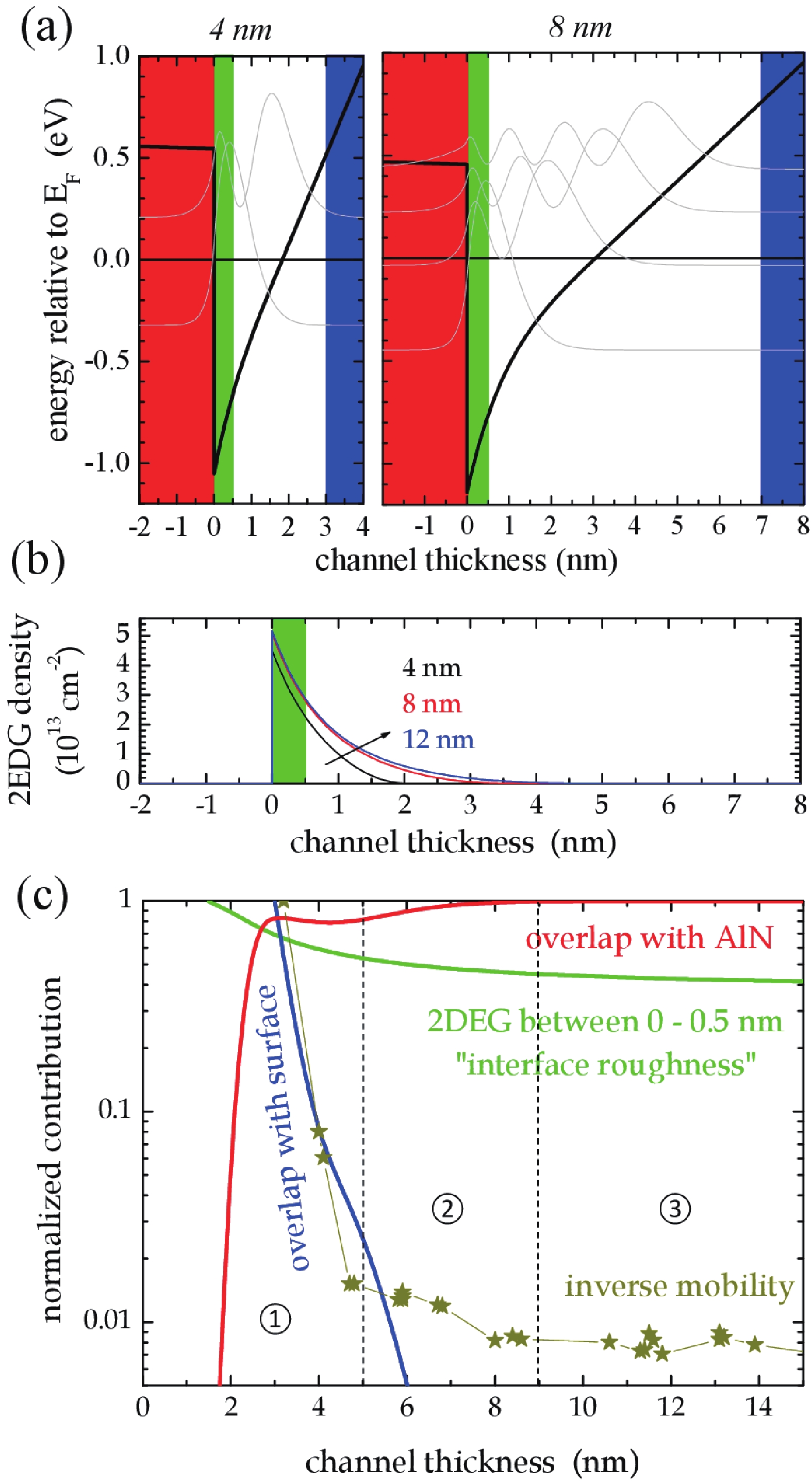
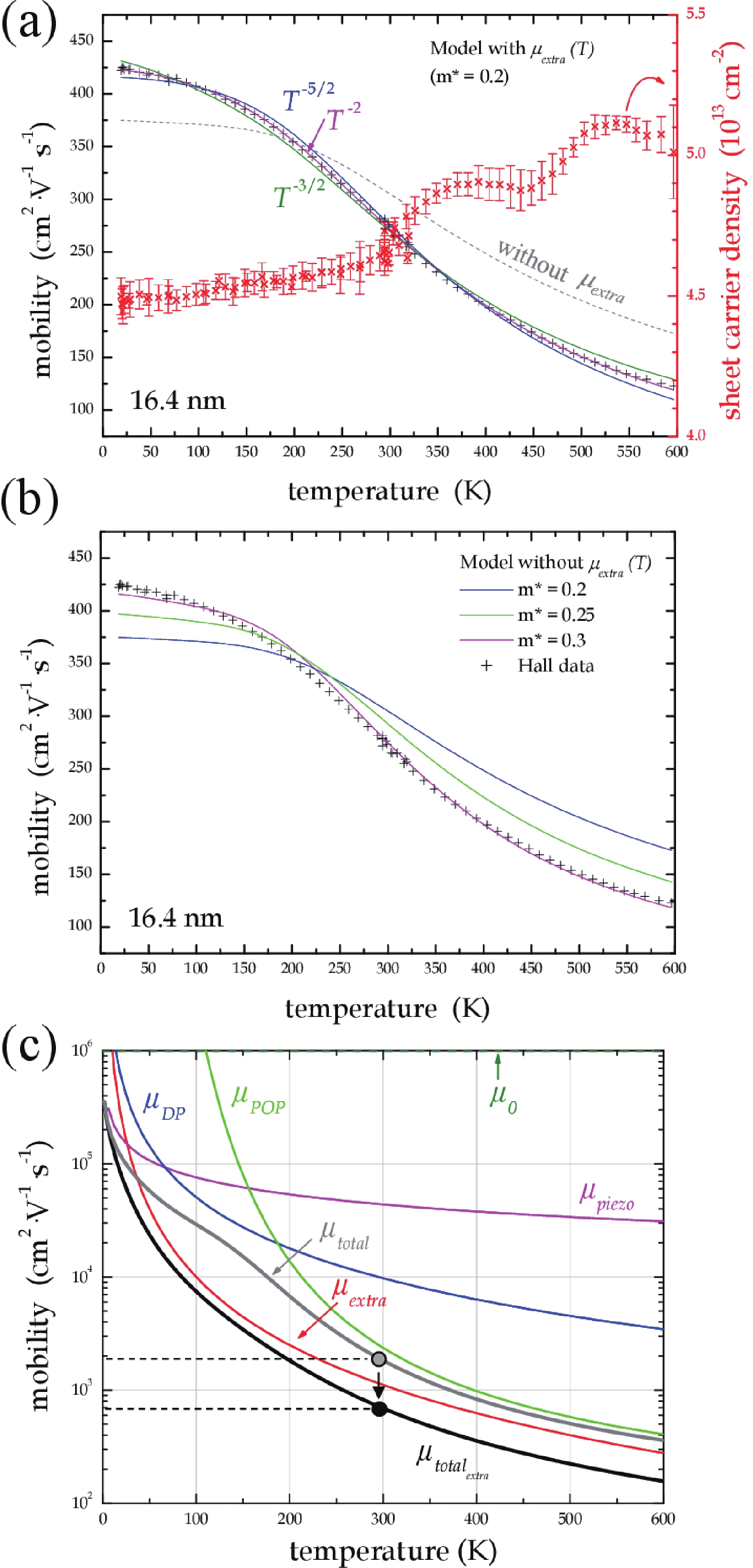
We have systematically studied the impact of thickness on the electrical properties of thin GaN channels on N-polar AlN (0001) templates grown on sapphire. The observed increase in sheet carrier density with increasing GaN thickness can be quantitatively reproduced by calculations assuming a Fermi-level pinning about 0.8 eV below the conduction band. The mobility strongly increases until 6 nm which correlates with reduced overlap of the 2DEG wave function with the surface layer. The mobility then increases more gradually up to 10 nm, corresponding to a reduced fraction of the 2DEG within the first 0.5 nm near the AlN/GaN interface, namely, the region affected by interface roughness. The mobility saturates at approximately 400 cm2·V−1·s−1, probably limited by dislocations and the overlap with deep traps inside the AlN back barrier. If the GaN thickness exceeds 15 nm, the mobility decreases, likely due to the onset of gradual relaxation and appearance of misfit dislocations. Finally, we note that the temperature-dependent mobility exhibits an unexpected contribution proportional to $ T^{-2} $ for all GaN channels on N-polar AlN, including those reported in the literature. Such observation may be explained by a 50% higher effective mass of the electron, which amplify the electron-phonon scattering, ultimately limiting the room-temperature mobility to about 750 cm2·V−1·s−1 and confining the sheet resistivity to values above 200 Ω/□.