Loading [MathJax]/jax/output/HTML-CSS/jax.js
J. Semicond. > 2018, Volume 39 > Issue 2 > 025001

SEMICONDUCTOR INTEGRATED CIRCUITS

A boosted negative bit-line SRAM with write-assisted cell in 45 nm CMOS technology

Vipul Bhatnagar1, Pradeep Kumar1, Neeta Pandey2 and Sujata Pandey1,

+ Author Affiliations

 Corresponding author: Sujata Pandey, email: spandey@amity.edu

DOI: 10.1088/1674-4926/39/2/025001

PDF

Turn off MathJax

Abstract: 
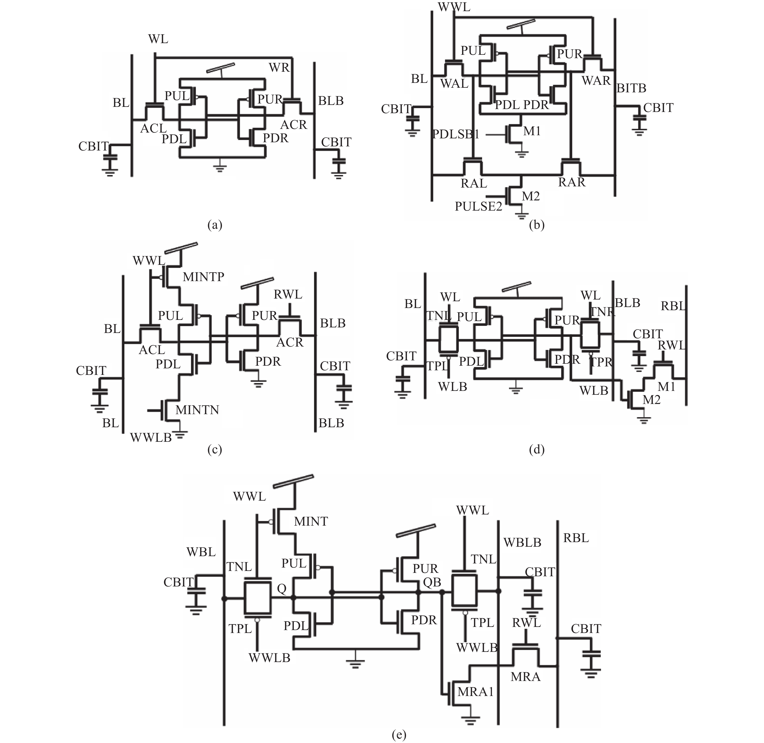
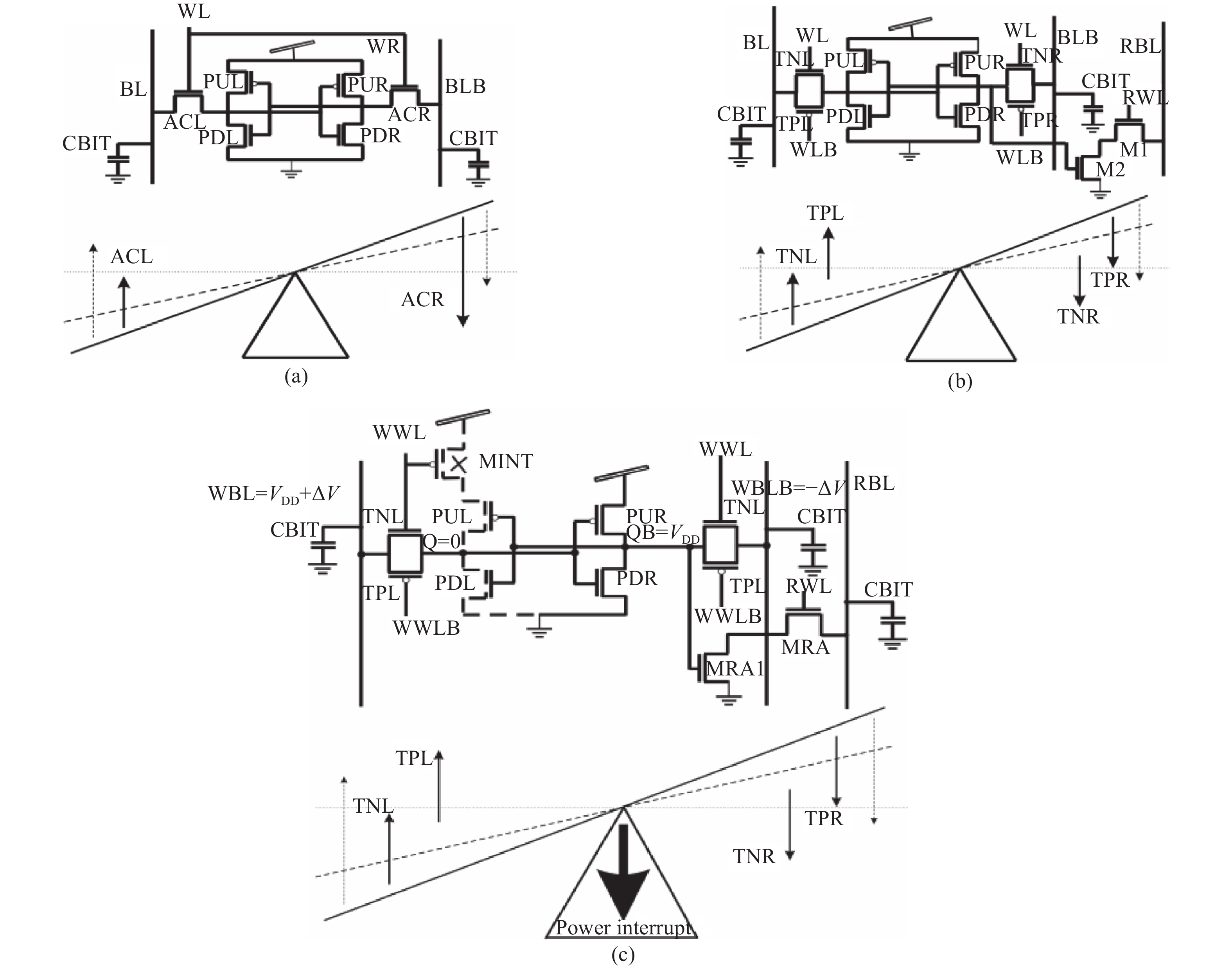
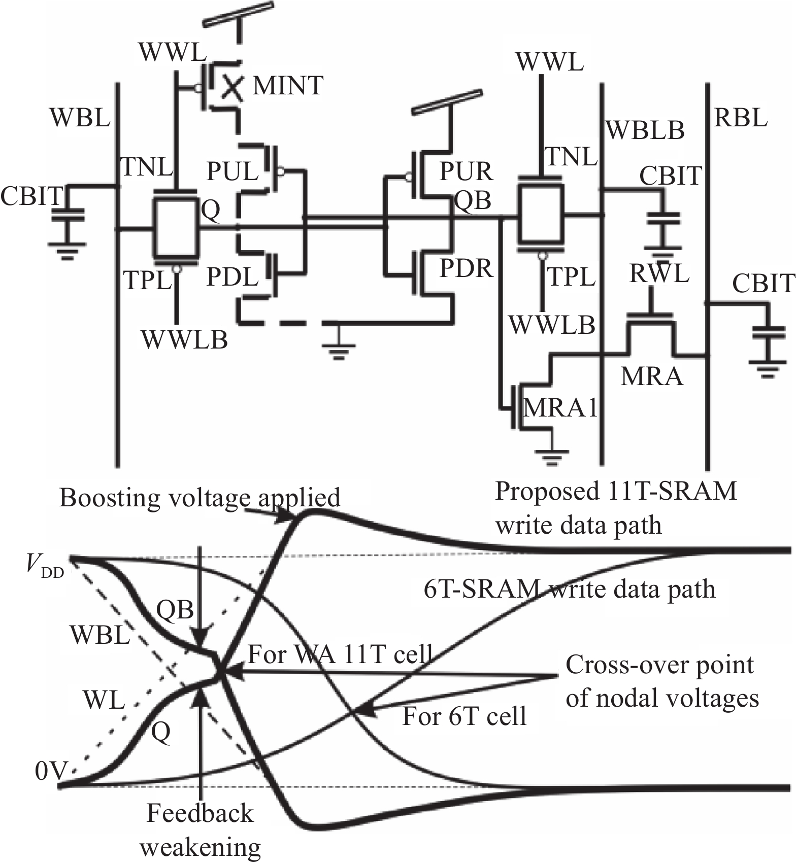
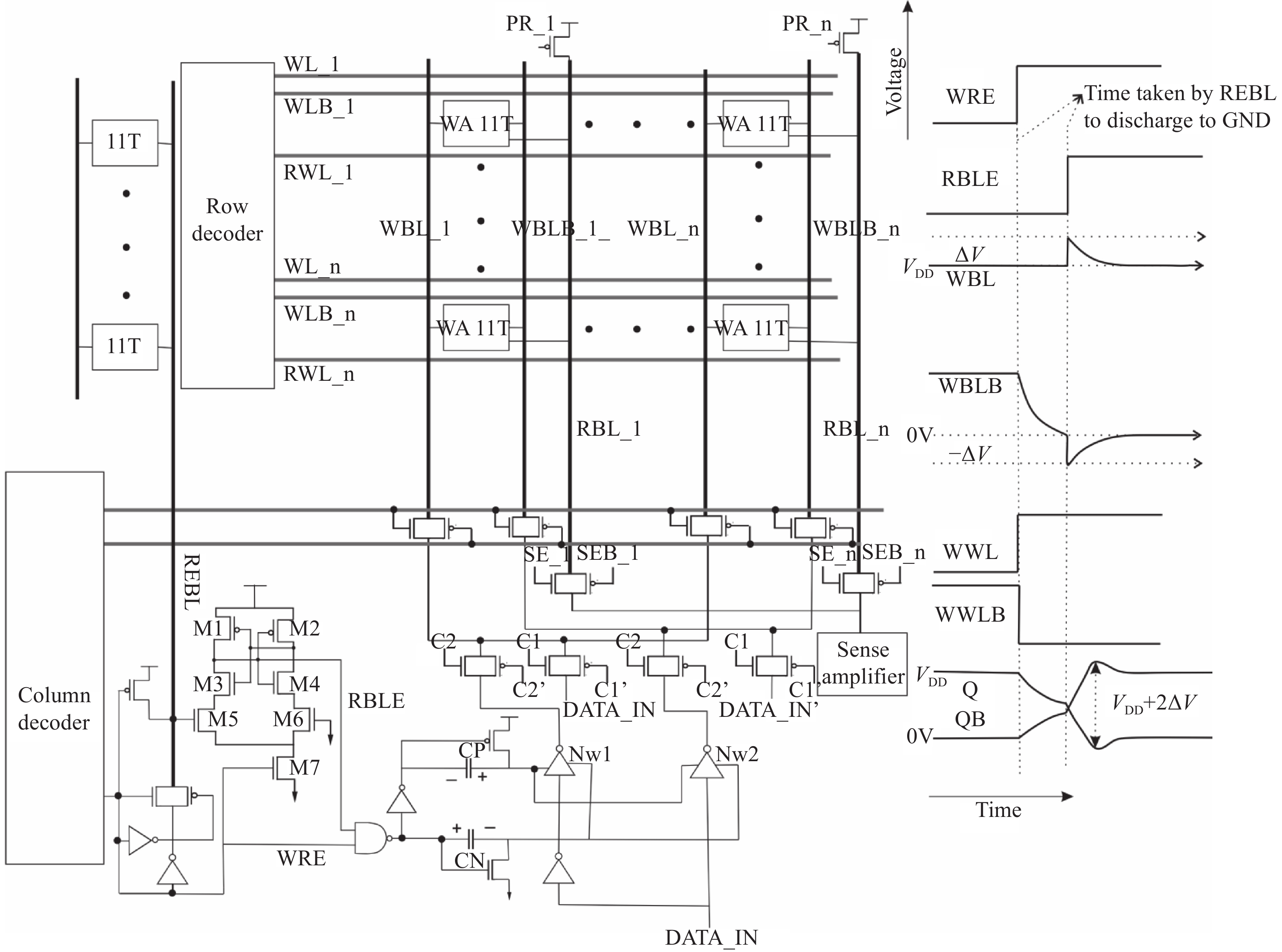
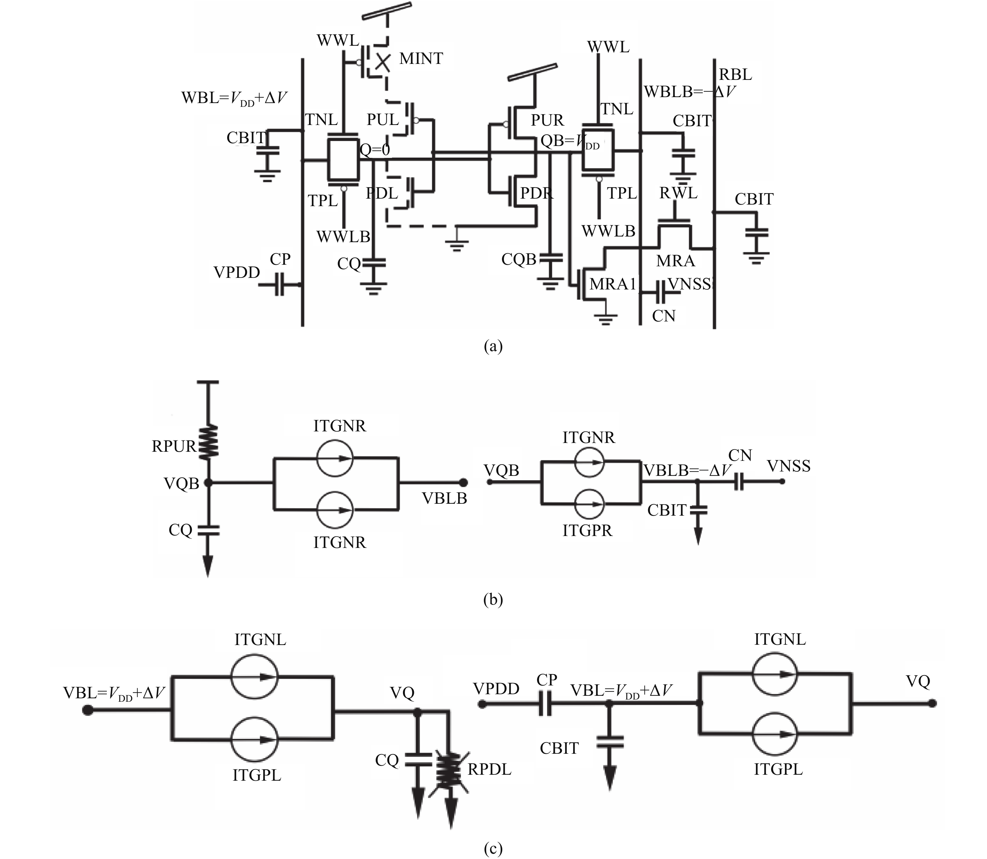
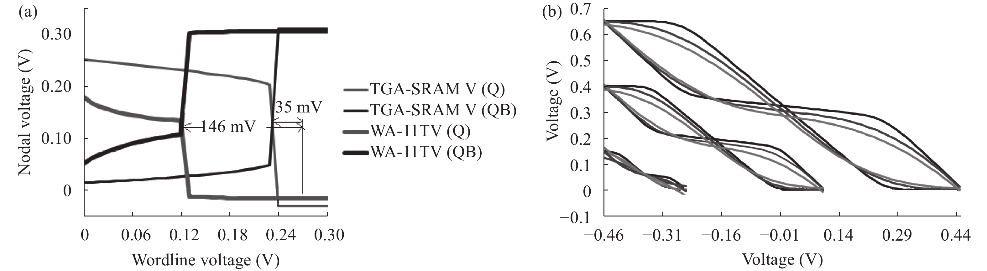
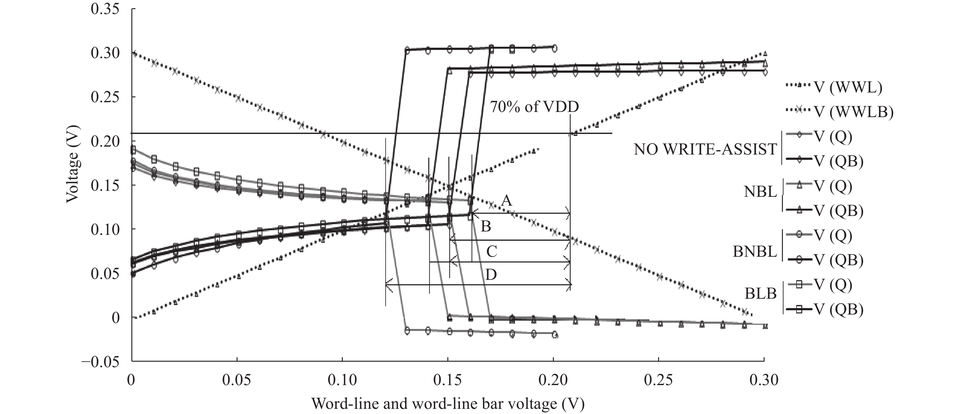
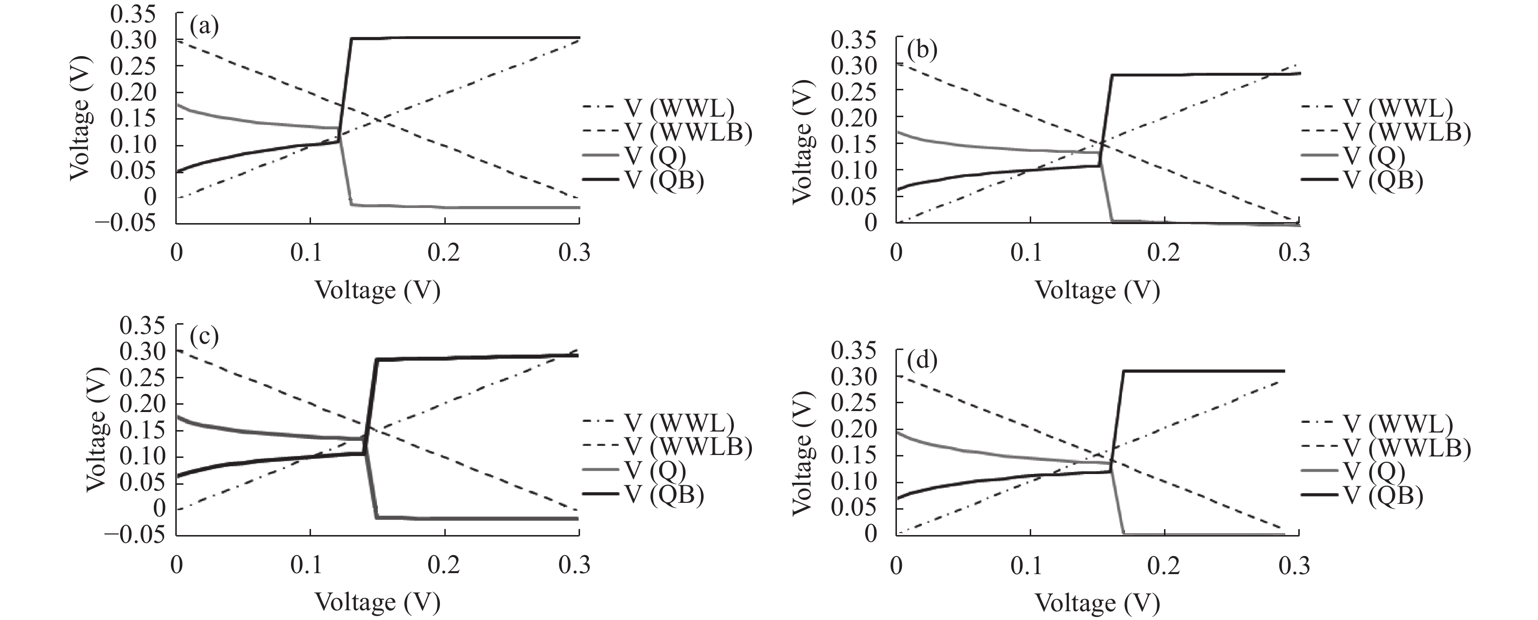
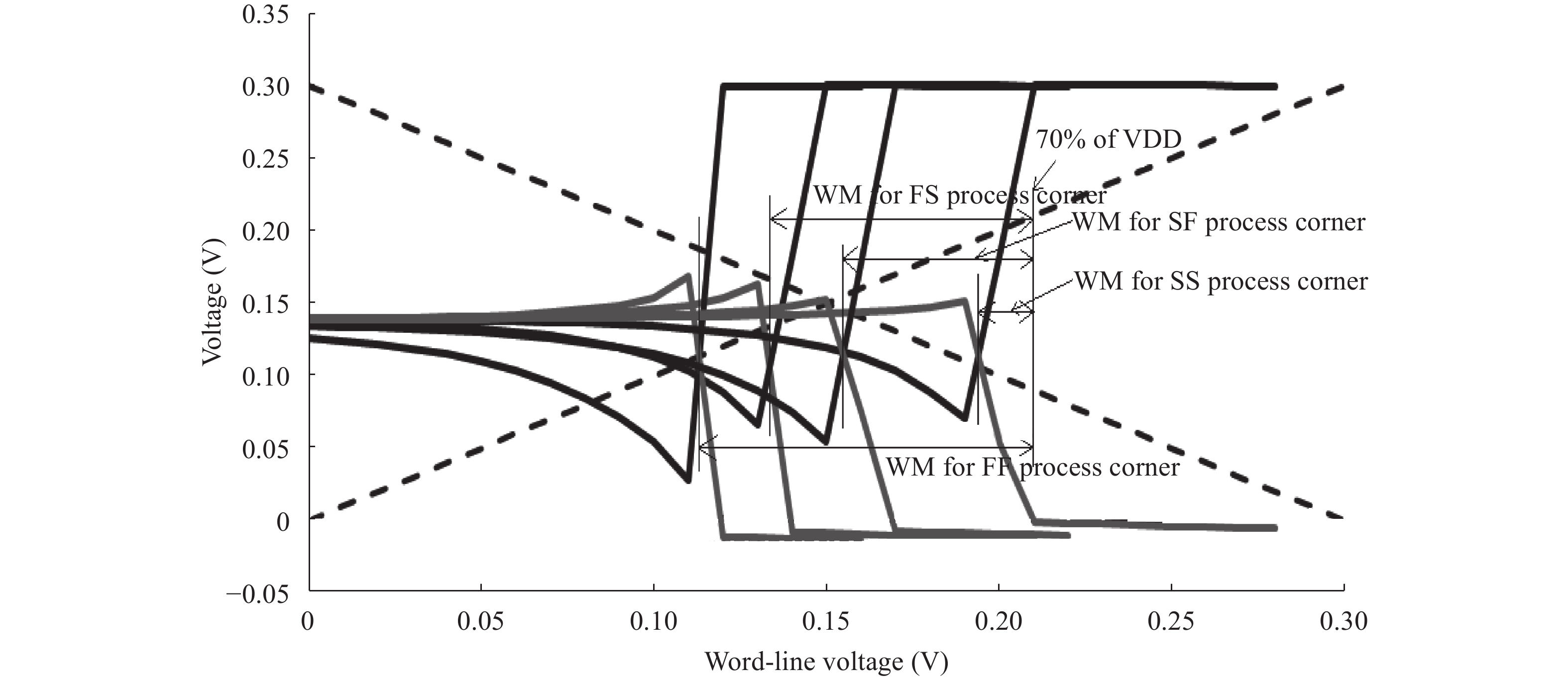
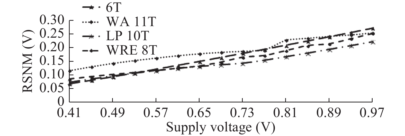
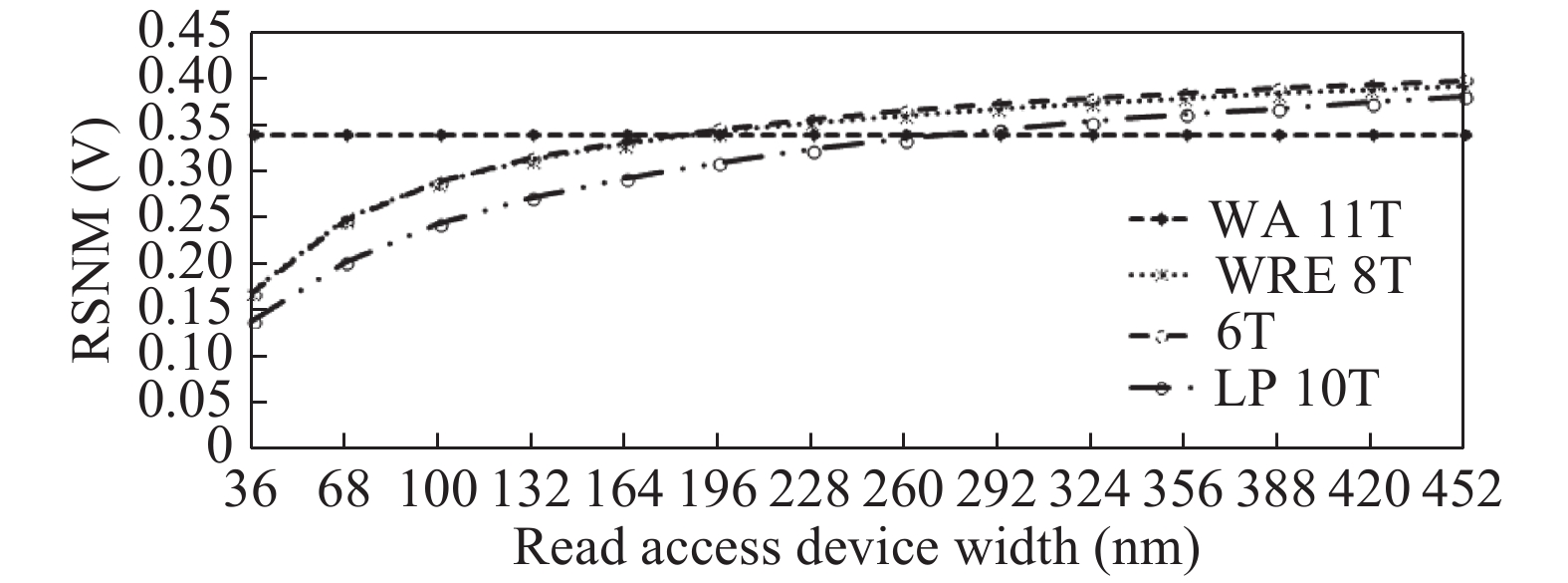
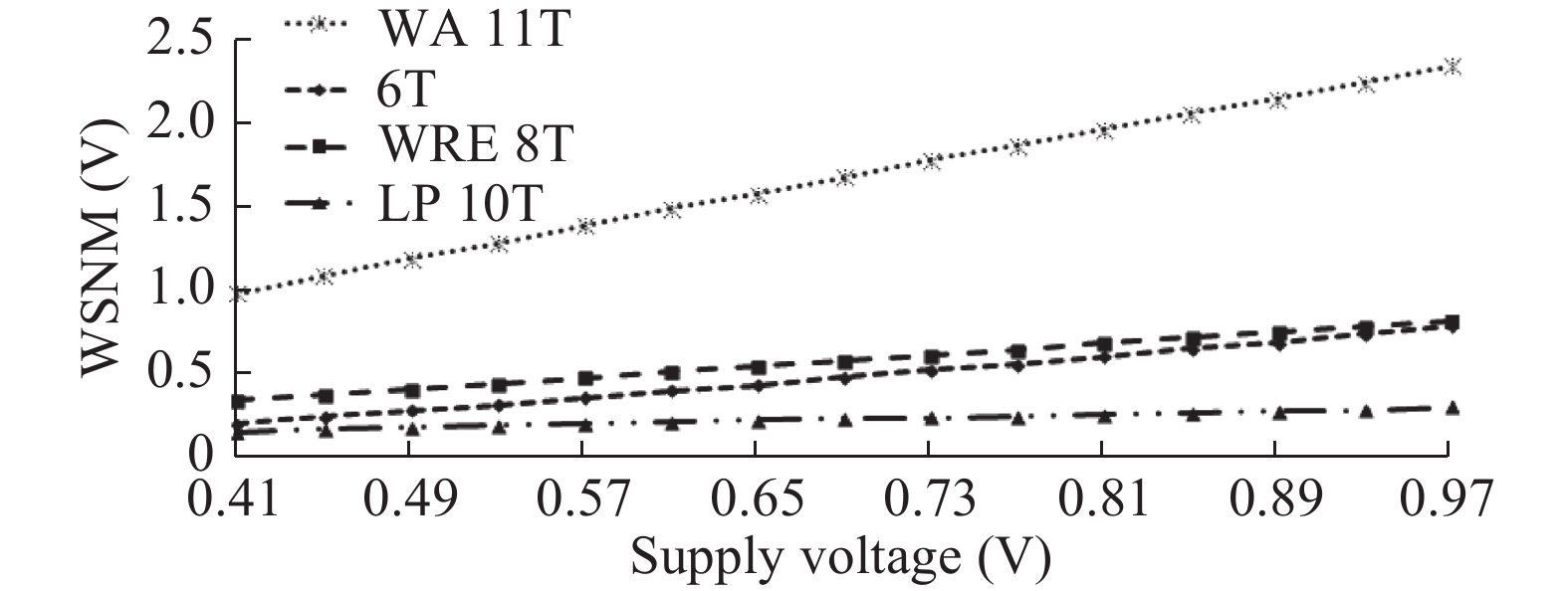
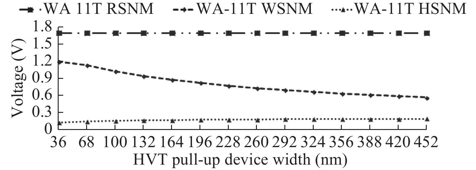
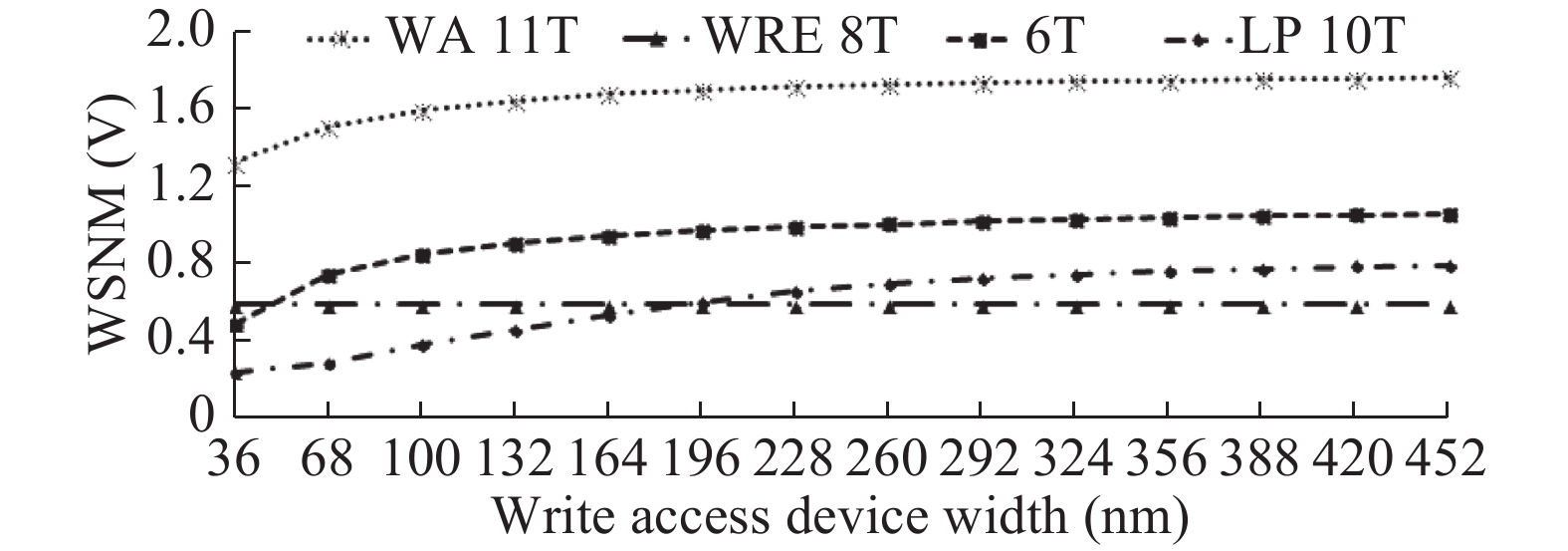
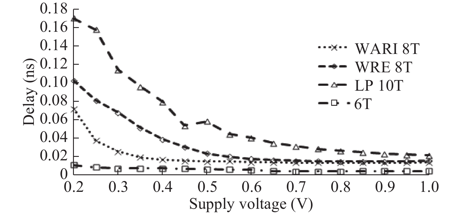
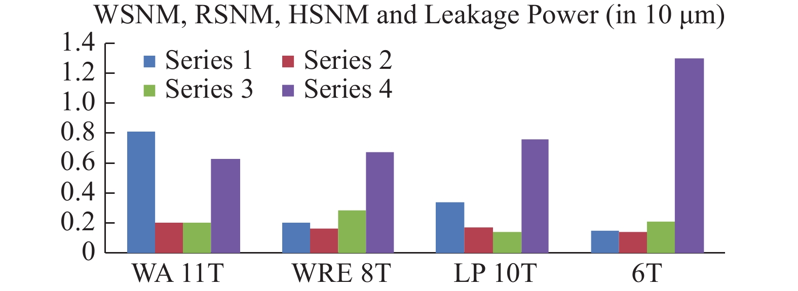
A new 11 T SRAM cell with write-assist is proposed to improve operation at low supply voltage. In this technique, a negative bit-line voltage is applied to one of the write bit-lines, while a boosted voltage is applied to the other write bit-line where transmission gate access is used in proposed 11 T cell. Supply voltage to one of the inverters is interrupted to weaken the feedback. Improved write feature is attributed to strengthened write access devices and weakened feedback loop of cell at the same time. Amount of boosting required for write performance improvement is also reduced due to feedback weakening, solving the persistent problem of half-selected cells and reliability reduction of access devices with the other suggested boosted and negative bit-line techniques. The proposed design improves write time by 79%, 63% and slower by 52% with respect to LP 10 T, WRE 8 T and 6 T cells respectively. It is found that write margin for the proposed cell is improved by about 4×, 2.4× and 5.37× compared to WRE8 T, LP10 T and 6 T respectively. The proposed cell with boosted negative bit line (BNBL) provides 47%, 31%, and 68.4% improvement in write margin with respect to no write-assist, negative bit line (NBL) and boosted bit line (BBL) write-assist respectively. Also, new sensing circuit with replica bit-line is proposed to give a more precise timing of applying boosted voltages for improved results. All simulations are done on TSMC 45 nm CMOS technology.

Key words: write-assist in SRAMboosted negative bit-linereduced write delaylow leakagereduced supply voltage

Moore’s law has long motivated scaling in CMOS technology, which has resulted in improvements in speed, power consumption and area. SRAM occupies large chip area and has a high activity factor which gives rise to large dynamic power dissipation. Linear reduction in supply voltage causes reduction of dynamic as well as leakage power dissipation but also reduction in speed. Also, increase in process variability causes an exponential increase in SRAM failure probability. This causes a decrease in write yield and read stability. At high supply voltage dynamic power dominates but at low supply leakage power becomes dominant due to exponential increase in cycle time. As operating frequency and packing density increase, speed, power consumption, noise immunity and low voltage operation become important for on-chip memories. SRAM is highly sensitive to process variations due to use of minimum geometry devices used to achieve high density. Variation from device to device over the same chip or from die to die over different chips can cause device mismatch and cause read stability, readability, write ability and cell stability degradation under data retention voltage (DRV). Moreover, there is a design trade-off between read stability and write stability.

Reduction in supply voltage is a preferred means of controlling leakage in SRAM and since it occupies up to 70% of the chip area[1], this leads to large savings in overall chip power but directly affects write ability. Over time a lot of new cell architectures[212] have been suggested that improve the stability of cell at the cost of chip area. The 8 T, 9 T, 10 T and 11 T[314] cells aim at improvement of read hold stability with the help of techniques like Schmitt trigger but adversely affect the cell ability to operate at reduced supply voltage and deteriorates below the ability of the basic 6 T cell. Write ability and delay are affected by reduced supply. Write noise margin and write yield are highly affected at scaled supply voltage and process variation makes it worse to an extent that write failure can result.

While 6 T cell shows the best possibility of data retention operation at reduced supply voltage, it suffers from poor stability during read and deteriorated write ability at scaled supply voltages. The WRE 8 T[8] cell offers improved read SNM of the cell due to separate read path and storage node isolation during read but suffers from the same reduced write noise margin as 6 T cell and added drawback of single bit-line read with inherently long access time. The LP 10 T cell[10] uses independent read and write paths thus offers no compromise in read and write margin due to access device sizing.

PPN-10 T cell[3] uses cascaded transistors in each of the back-to-back inverters although offers reduced leakage both from supply and data dependent bit-line leakage but requires higher voltage head-room and thus limits the level to which supply can be scaled. Fig. 1 shows some of the existing SRAM cell topologies available in literature.

Fig. 1(a) shows the basic, widely used 6 T SRAM cell, Fig. 1(b) shows LP 10 T cell, Fig. 1(c) WRE 8 T cell and Fig. 1(d) shows transmission gate assist SRAM cell. The TGA-8 T cell offers improved write ability and write SNM at reduced supply voltage and at the same time provides a read path that is separate from storage nodes and thus offers improved read stability and read SNM.

In this paper, an 11 T SRAM cell is proposed, as shown in Fig. 1(e) which is suitable for boosted-negative bit-line technique and has significant improved write yield and write noise margin. The proposed cell uses transmission gate access transistors, which has improved write strength over the simple NMOS access device. Also, the PMOS device connected in cascade with the left inverter interrupts the supply to weaken the feedback loop and assist in write operation. The read access path does not include the cell nodes and thus exhibits a superior read SNM and read stability.

Figure  1.  (a) 6 T SRAM cell, (b) LP 10 T cell[10], (c) WRE 8 T cell[8] and (d) TGA-8 T cell[5], and (e) the proposed WA 11 T cell.

The write operation on 6 T cell with conventional write path, TGA-SRAM cell[26] and proposed WA 11 T cell with TGA and power supply interrupt are shown in Fig. 2.

Figure  2.  Write operation on (a) 6 T cell with conventional write path, (b) TGA-SRAM cell[26], and (c) the proposed WA 11 T cell with TGA and power supply interrupt.

In 6 T cell, access devices connected to the cell nodes in the write path perform a see-saw action with two stable states. Let us assume that the node Q holds a logic 0 and node QB holds a logic 1. Changing the state of the cell is possible by applying force to either one side of the see-saw (with increased delay and reduced WSNM) or applying force to both the sides simultaneously (which eases the write operation of SRAM cell equivalent to write improvement). At the start of the write cycle, both the access devices ACL and ACR conduct with equal strength since VGS-ACL = VGS-ACR = VWL. But, as the voltage on the node Q starts to rise, VGS-ACL starts to decrease resulting in reduced strength of the ACL with ACL reaching cut-off at VQ = VWLVTHN i.e. VGS-ACL = VTHN. On the other hand, ACR continues to write with the same strength throughout the write operation. Thus, for the 6 T SRAM, write operation is mostly carried-out by the access device connected to node storing a logic ‘1’, which becomes a focus for write-assist.

Write-assist techniques can be divided into following types, namely:

(1) Changing magnitude and or duration for which noise source is applied[1316].

(2) Reduction in the latch strength or change in transfer characteristics[17, 18].

(3) Use of masking or architectural methods.

Numerous publications have devoted a lot of effort on the write-assist techniques like raising global VDD, reducing theVDD at cell, raising VSS at cell, word line boosting, boosting voltage at BL and BLB, increasing the strength of access device, weakening of the pull-up device of cell and interrupting to weaken feedback by use of pass transistor or TG.

With raising of the global VDD, current driving ability of access devices improves. Reduction in VDD or raising of VSS of the cell during write weaken the latch and write with reduced resistance. Strengthening of access devices with respect to cell by either boosting of the word line (WL) or BL-BLB voltages for weakening of the pull up device of the inverters leads to improved write-ability of the cell.

Reduction in the write bit-line voltage from 0 to −∆V (where ∆V represents magnitude of voltage boost in positive and negative direction) leads to write-ability improvement of the cell by improvement of VGS and strengthening of the access transistor without any effect over the latch inverters.

WL boosting and latch weakening by either VDD collapse or VSS raising or by using pass device or TG in the inverter positive feedback loop either lead to poor hold SNM or stability of half-selected cells and require very power-costly control of global VDD or elaborate control of local VDD or are unsuitable for reduced supply voltage.

Application of a negative voltage −∆V instead of ground leads strengthening of the access device connected to cell node storing a high voltage and considerable improvement of write-ability of the cell[1925]. Negative bit-line voltage has been produced by the use of CBoost instead of a separate negative voltage generator charge pump circuit. The CBoost with the optimum value of charge is applied to the low write bit-line at appropriate time for maximum negative swing in bit-line voltage. For determining the appropriate time, when discharge of the capacitive bit-line to a voltage as close to zero as possible, a separate replica bit-line (capacitance monitor) is used. The replica bit-line, having the same capacitive load CBL as the actual bit-line and they being connected together, has capacitance of CBL. The bit-line will discharge completely when the replica bit-line discharges to Gnd.

Design proposed in Ref. [18] uses replica bit-line and replica buffer to determine the time when Cboost should be connected to bit-line. REBL together with the delay block is used to determine the time when boosting capacitor should be connected to the bit-line. The boosting capacitor Cboost is connected to the ground of negative going bit-line to produce a negative voltage on the low going bit-line. Mukhopadhyay et al.[17] proposed the structure where the Cboost capacitors were coupled to the bit lines BL and BR respectively and they assist appropriate bit-line in reaching a negative voltage level.

In this section first WA 11 T cell is discussed followed by a detailed description of the proposed negative bit-line technique.

The proposed WA 11 T cell with nodal voltages and word-line voltages of the cell is shown in Fig. 3. To improve ACL conduction, NMOS access devices on both sides of the cell are replaced by a TG (TPL+TNL and TPR+TNR) on both sides of the cell. This lets us apply write-assist to both sides of the cell and conduction throughout the write operation. As the write operation starts, VGS for the TNL starts to decrease as the voltage builds up over the node Q, but for the TPL, device, VGS-TPL = VWBLBVWWLB remains constant with rise in VQ and thus, TPL (with its source connected to the bit-line) continues to conduct with maximum strength throughout the write-operation. TG allows write-assist technique to be applied from both sides of the cell simultaneously thus significant improvement in write operation.

Figure  3.  Proposed WA 11 T cell and nodal voltages and word-line voltages of WA 11 T cell.

NMOS access device is able to conduct only for the duration when its VGSVTHN i.e. it will stop conducting when voltage of the cell node rises up to the point that VGS becomes less than VTHN when the condition for conduction of the NMOS pass device is no longer met. Thus, the pass device writing 1 into the cell node does not conduct for the last remaining part of the write operation and only the NMOS pass device connected logic 0 bit-line conducts and completes the write operation.

In the proposed design, TG is used in place of a simple pass device to ensure rapid charging of cell node where logic 1 is being written since one of the two devices (NMOS or PMOS) will remain in saturation when the other enters triode region. This provides a constant current capability to the TG and ensures faster and uniform charging rate of both the cell nodes throughout the write operation, since in the proposed design, access devices connected to both bit-lines conduct with maximum strength even in the last lean period of the write operation.

Also, focus is on the reduction of the strength of holding the last data during write operation by the SRAM cell. The strength with which SRAM cell holds the last stored value depends on the feedback strength between inverters of the cell. By reducing the feedback strength, a new data value can be written to the cell with a much reduced effort. This is done by interrupting the supply to one of the inverters during the write operation temporarily. Power supply is interrupted to the left inverter using device MINT with its gate connected to the WWL which will be shown later.

The TG access thus charges the node Q of the cell with maximum strength throughout the write operation. The write delay and dependence over process variability is reduced and write SNM and write yield are improved considerably. This also allows write assist technique to be applied to both sides of the cell i.e. applying force over both sides of the cell simultaneously, which leads to significant write-ability improvement. A pMOS device M1 is connected to the left inverter of the proposed cell whose Gate is connected to write word line, since the power supply to the left inverter is interrupted by MINT during write operation, which leads to weakening of the feedback strength and significant improvement in write-ability of the proposed cell.

The 6 T cell suffers from poor write ability and the increase of the strength of access devices improves WM and write delay since they have to overcome the positive feedback of inverters. On the other hand, high strength of pass devices leads to a reduced stability of the cell during read and read SNM. To overcome reduced read SNM due to improved strength of access devices, 8 T cell uses a separate read path that does not include the cell nodes. The proposed cell uses the similar structure to provide node isolation during read operation. Thus, the conflict of transistor sizing for access devices is addressed. The proposed cell is isolated from the read bit-line so that maximum stability during read operation is guaranteed.

Fig. 4 shows the proposed 11 T array having n-rows and n-columns. Capacitors CP-Boost and CN-Boost are used to produce a voltage of VDD+∆V and −∆V over the bit-lines WBL and WBLB. The replica bit-line consisting of n-rows of 11 T cells are used to determine best time for connecting the boosted positive and negative voltages to the write bit-lines. A capacitance of CBL is realized by the REBL, which is pre-charged to VDD before each write operation. REBL is discharged to Gnd using the inverter with WRE signal, which goes high (at start of write operation) as its input.

Figure  4.  Boosted negative bit-line write-assist technique.

A voltage sensing circuit is used (M1–M7) where M1, M2, M3 and M4 make back-to-back inverters and M5 and M6 (biased to operate in saturation) form a differential pair that makes the sensing circuit more sensitive than inverter[19]. WRE connected to gate of M7 enables the voltage sense circuitry (M1–M7), which compares the REBL voltage with Gnd. The dummy bit-line, which is pre-charged to VDD, discharges towards Gnd through the inverter whose input is WRE. The voltage sensing circuit formed by M1 to M7 whose one of the input is connected to the gate of transistor M5 compares the dummy bit-line voltage with gnd.

The input of the NAND gate goes high as soon as dummy bit-line voltage discharges to Gnd. Since the other input to the NAND gate WRE is already high, thus the output goes low, which is applied to the inverter input. As the output of inverter goes high, it comes in series with the CP-Boost capacitor, which leads to 2VDDCP-Boost/CBL voltage to appear at the WBL through the inverter NW1 when appropriate control signals are activated. Similarly, −VDD × CN-Boost/CBL appears at the WBLB during write operation.

Control signal C2 goes high (control C1 goes low) to discharge the WBLB towards Gnd and word-line decoder output WWL and WWLB goes high and low respectively. This interrupts the supply to the left inverter of SRAM cell and turns-on devices of both TGs.

As the voltage over the bit-lines (WBL and WBLB) loaded with CBIT slowly change towards VDD and Gnd respectively, voltage over input and output nodes of the right inverter begin to change (node QB discharges towards 0 and Q charges towards VDD). Meanwhile, the boost capacitors CP-Boost andCN-Boost are charged using pMOS and nMOS which are ON. Output of voltage sensing circuit RBLE signal goes high when REBL discharges to VDD/2 which indicates that write bit-lines have also discharged to gnd. Control signal C1 goes high (C2 goes low) and applies the boosted signals (VDD + ∆V and −∆V) to the WBL and WBLB through the inverters NW1 and NW2 respectively.

· Voltage boosting (on both the cell nodes in opposite directions) increases |VGS| of TG devices giving them higher strength thus increasing slope of charging of cell nodes. Source of TPL is connected to VBL = VDD + ∆V(voltage boosting) and source of TNR connected to VBLB = −∆V (negative bit-line voltage) during write operation which improves write-ability, write time and WSNM.

· With weakening of the feedback, (due to the left inverter turned off) the rate of charging of node Q and node QB has increased providing an improved WM faster write-ability.

· Use of a new voltage sensing circuit (M1–M7) with more precise timing that improves boosted bit-line voltage (unlike a simple inverter IN[19]) and helps to lower value of boosting capacitor for the same WM improvement.

· Due to feedback weakening, reduced amount of boosting voltage is required for write improvement, which reduces effect over the half-selected cells of the same column.

· Feedback weakening in WA 11 T reduces voltage boosting amount required for the same WM improvement as earlier suggested techniques to address the issue of reliability degradation of access devices due to increased VGS (boosted and negative bit-line voltage).

The proposed WA 11 T cell during write operation is shown in Fig. 5(a) and its simplified equivalent model of proposed SRAM cell is shown in Figs. 5(b) and 5(c) respectively.

Figure  5.  (a) Proposed WA 11 T cell during write operation (node Q at 0 and node QB at VDD). (b) Model of the proposed WA 11 T cell (node QB). (c) Model of the proposed WA 11 T cell (node Q).

Assuming node Q stores logic ‘0’ and QB stores logic ‘1’, the write operation of cell is modelled in two parts to consider both left and right inverters asymmetrical cell structure.

1. PUR device is modelled as a resistor RPUR since it operates in triode region. Capacitance at node QB is modelled as CQB. CBLB and CN are the total capacitance of BLB. Since TNR and TPR operate in saturation thus they are modelled as constant current sources.

CQBdVQBdt=IPURITGNRITGPR, (1)
IPUR=VDDVQBRPUR, (2)
ITNR=βTNR2(VDDVBLBVthn)2, (3)
VQB=(|bR|bR24aRcR)ZeaRtbR24aRcR+bR24aRcR|2a|(ZeaR.tCQBbR24aRcR1), (4)

where aR=βTPR2 ,

bR=βTPR|VHP|1RPUR,cR=VDDRPURβTPR2VTHP2βTNR2(VDDVBLBVTHN)2,Z=|2aRVDD+bR+bR24aRcR2aRVDD+bRbR24aRcR|,RPUR=1βPU(VDDVQ|VTHP|),(5)

where the details of various parameters are well available in literature.

2. Since supply to left inverter is interrupted, devices node Q are modelled as capacitance CQ. Devices TNL and TPL are modelled as constant current sources. Boosting capacitance and BL capacitance are represented by CP and CBIT at node QB of the cell.

CQdVQdt=ITNL+ITPL, (6)
ITGNL=βTNL2(VDDVthn)2, (7)
ITGPL=βTPL2(VBL|Vthp|)2, (8)
VQ=(|bL|bL24aLcL)(1eaLtCQbL24aLcL)|2a|(1|bL|bL24aLcL|bL|+bL24aLcLeaLtCQbL24aLcL), (9)

where

aL=βTNL2,bL=βTNL(VDDVTHN),cL=βTNL2(VDDVTHN)2+βTPL2(|VBL||VTHP|)2.

There is an attempt to write node Q, assumed to store logic ‘0’ and logic ‘1’, in BNBL-WA cell. Improvement in the proposed circuit is seen as faster increase of nodal voltage VQ given by Eq. (9). aL and cL are positive whereas bL is negative. Factor cL depends on bit-line voltage VBL, which is increased due to the boosted bit-line technique.

Value of bL reduces to less than[19] in the suggested BNBL-WA 11 T. PDL device in operating in triode earlier (as in Ref. [19] with Q = 0 and QB = VDD) due to interrupted supply to the left inverter, RPDL becomes infinite, thus 1/RPDL becomes 0, which causes reduction in bL. cL increases with the increase in VBL (BL voltage boosting) causing an increase in value of cL. Here, increment and decrement in each of the terms is shown by ↑ and ↓ within parenthesis in numerator and denominator of Eq. (10). bL reduces whereas cL increases which causes both first and second terms in the numerator to increase. Whereas, denominator decreases, which shows faster increase in VQ compared to 8 T cell[5] and BNBL technique of Ref. [19].

VQ=()(1↓↓)|2a|.(1↓↓). (10)

In 6 T or 8 T[5] SRAM, charging of node Q is done by the back-to-back inverters, whereas here, due to supply cut-off to the left inverter and breaking of the feedback loop by switching off MINT, node Q (input to the right inverter) is charged directly by the TPL of TG and QB (output of the right inverter) is discharged directly by TNR of TG without being opposed by feedback of the cell.

· Here, write operation takes place without being resisted by the feedback within cell (like in the conventional 6 T or 8 T cell[5] or BNBL technique[19]).

· Boosting of the bit-line voltage causes increase in strength of access devices thus a faster charging of node Q and discharge of node QB giving an improved write margin and write-ability to the proposed design than Ref. [19].

Simulation at 45 nm CMOS technology was done to compare BNBL-WA 11 T, WRE 8 T, conventional 6 T and LP 10 T cells.

Fig. 6(a) shows plot of the word-line voltage versus nodal voltages for dc analysis of BNBL WA 11 T and TGA 8 T cells.

The simulation was done for BNBL WA 11 T and TGA 8 T cells at supply voltage of 0.3 V and boosting of 9% and 20% applied to the cell respectively. Write-margin is calculated as the difference between 90% of the final word-line voltage (i.e. 0.27 V) and cross-over point of nodal voltages. The WM of 146 and 35 mV for BNBL WA 11 T and TGA 8 T cells respectively was obtained. An improvement of 70% in WM compared to Ref. [5] provided improved write-ability with reduced amount of boosting required. Fig. 6(b) shows parametric sweep analysis for read operation of WA-11 T for supply voltages of 0.15, 0.4, and 0.65 V and temperatures of −125, 260, and 650 °C respectively.

Figure  6.  (a) DC analysis for proposed 11 T cell and TGA 8 T cell use (with 9% and 20% BNBL voltages respectively) showing nodal voltages and WM and (b) parametric sweep analysis for read operation of WA-11 T for supply voltages of 0.15, 0.4, and 0.65 V and temperature of −125, 260, and 650 °C respectively.

In this section, we compare BNBL, NBL, BBL (boosted bit-line) and no write-assist techniques when applied to the proposed WA 11 T SRAM. Ground boosting and VDD collapse are not included since these techniques have inherent drawbacks. Boosting ground voltage leads to reduced VDS of access devices connected Q and increases trip point of the right hand side inverter. On the other hand, cell VDD collapse technique decreases VDS of access device connected to QB and increases the trip point of the right inverter.

Write margin of the WA 11 T cell has been calculated using different techniques[24]. Since most of the suggested write techniques depend on low-going bit-line connected to side of SRAM cell, most techniques consider low-going bit-line for WM calculation. To take into consideration the effect of both bit-lines we consider write word-line voltage sweep (WWL from 0 V to VDD and WWLB from VDD to 0 V are swept together) and consider the point at which flipping of the state of inverters connected to the cell nodes occurs. We consider WM as the difference between points when write word-lines achieve 70% of their final value and the cross over points of the nodal voltages[24, 25].

In Fig. 7, DC analysis has been performed for word-line voltage sweep from 0 to VDD and negative bit-line, boosted bit-line, boosted negative bit-line and with no write-assist are applied to the WA-11 T cell. WM was found as A, B, C and D for BNBL, no-assist, NBL and BBL respectively. Here WM is defined as the difference in voltage between nodal cross-over point and 70% of maximum word-line voltage and gives the measure of margin against write failure.

Figure  7.  DC analysis for word-line voltage sweep from 0 to VDD and VDD to 0 for (a) negative bit-line, (b) boosted bit-line, (c) boosted negative bit-line, and (d) no write-assist being applied to the proposed WA-11 T cell.

In the proposed design (Fig. 8, use of WA-11 T with BNBL) with a VDD of 0.3 V, boosted and negative voltage of 0.325 V and −0.025 V, i.e. 9% boosting is used. WM for BNBL, no write-assist, NBL and BBL were found to be 0.095, 0.05, 0.066, and 0.03 V respectively. BNBL provides 47%, 31%, and 68.4% improvement in WM (mentioned in Table 1) with respect to no write-assist, NBL and BBL respectively.

Figure  8.  DC analysis for word-line voltage sweep from 0 to VDD and VDD to 0 for (a) boosted negative bit-line, (b) no write-assist, (c) negative bit-line, and (d) boosted bit-line being applied to the proposed WA-11 T cell.
Table  1.  Write-margins and write-time obtained for different write-assist techniques used with WA 11 T cell.
Write-assist technique
(used with WA-11 T cell)
BNBL No assist NBL BBL
Write-margin (mV) 95 50 66 30
Write-time (ps) 9.3 23 27.9 63
DownLoad: CSV  | Show Table

Thus, BNBL was found to be the best write-assist technique to improve write margin. With less than half of the boosting and negative bit-line voltages applied (considering 20% boosting at VDD of 1V used in Ref. [19]), much higher improvement in WM was obtained. This is attributed to the collapse in the feedback strength within cell which enables faster writing into the proposed WA 11 T cell.

The proposed technique requires much smaller value of boosting capacitor and the area overhead for the same improvement in WM as Refs. [1719]. Also, with the reduction in value of boosting, the reliability issues associated with access devices have been addressed, which nag other suggested write-assist techniques based on boosted and negative bit-line voltages.

Fig. 9 shows simulation of write margin for BNBL WA 11 T cell for all four process corners i.e. FF, FS, SF and SS. Table 2 gives the write margin and write-time obtained for the WA 11 T cell.

Figure  9.  Write margins for proposed BNBL WA 11 T scheme for process corners.
Table  2.  Write-margin and write-time for proposed BNBL WA 11 T scheme for FF, FS, SF and SS process corners.
Process corners FF FS SF SS
Write-margin (mV) 99 76 54 16
Write-time (ps) 8.9 17.2 20.6 127
DownLoad: CSV  | Show Table

Write margin is calculated with the difference in voltage between point when write word-lines reach 70% of VDD to the nodal voltage cross-over point of cell. Write margin for FF, FS, SF and SS process corners were found to be 0.099, 0.076, 0.054, and 0.016 V respectively. The write margin for FF process corner is 1.26 ×, 1.78 × the FS and SF process corner margins. Write-time for FF, FS, SF and SS were found to be 8.9, 17.2, 20.6, and 127 ps respectively. Write time for FF was found to be only 51.8% and 43% of FS and SF process corners respectively.

Fig. 10 is supply voltage versus RSNM for 6 T, WA 11 T, LP 10 T and WRE 8 T cells. Read noise margin for WA 11 T is also significantly higher than the other cell in the supply voltage range of 0.49 V to 0.89 V. RSNM was found to be 1.2 ×, 1.42 × and 1.24 × higher than the WRE8 T, LP10 T and 6 T cells respectively, while LP10 T has the least RSNM and the same trend is followed with the entire range of supply voltage.

Figure  10.  Supply voltage versus RSNM for 6 T, WA 11 T, LP 10 T and WRE 8 T cells.

In Fig. 11, the variation of read access device aspect ratio from 1.125 to 14 showed a constant RSNM for the WA-11 T cell whereas a lot of variation in RSNM for all the other cells. An improvement of 2.09 ×, 5.24 × and 2.53 × as compared to WRE8 T, LP10 T and 6 T cells respectively at aspect ratio of 1.125 for read access device was observed.

Figure  11.  Read access device width versus RSNM for 6 T, WA 11 T, LP 10 T and WRE 8 T cells.

Fig. 12 plots supply voltage varied between 0.41 and 1 V versus WSNM for WA 11 T, WRE 8 T, conventional 6 T and LP 10 T cells. The WSNM for WA 11 T was found to be improved by 2.4 ×, 5.36 × and 4.1 × compared to WRE8 T, LP10 T and 6 T respectively at supply voltage of 0.4 V.

Figure  12.  Supply voltage versus WSNM for 6 T, WA 11 T, LP 10 T and WRE 8 T cells.

Fig. 13 MINT device width versus SNM is plotted for read, write and hold. Write SNM shows a gradual reduction with increase in MINT width. This reduction is due to increase in strength of feedback with width of MINT, which makes it harder to write.

Figure  13.  MINT device width versus SNM.

Fig. 14 plots write access devices of TG channel ratio varied from 1.125 to 14 and WSNM was found to be constant for BNBL-WA 11 T and WRE8 T cells and 2×, 5.02× and 2.52× higher than WRE8 T, LP10 T and 6 T respectively.

Figure  14.  Write access device width versus WSNM for 6 T, WA 11 T, LP 10 T and WRE 8 T cells.

Variation of leakage power with supply voltage is shown in Fig. 15. Variation of write power dissipation with supply voltage from 0.41 to 1 V has been plotted on a logarithmic scale in Fig. 16. There is a 24×, 6.3× and 46.6× times reduction in the write power for BNBL-WA 11 T at 0.41 V supply compared to WRE8 T, LP10 T and 6 T respectively. The write power increases more rapidly than the other cells but continues to stay lowest among the four cell for BNBL-WA11 T from supply voltage of 0.41 to 0.55 V, then exceeds the power for LP10 T cell but is still lower than WRE8 T and 6 T cells. The WRE8 T still continues to consume power lower than the 6 T cell.

Figure  15.  Supply voltage versus leakage power for 6 T, WA 11 T, LP 10 T and WRE 8 T cells.
Figure  16.  Supply voltage versus write power for 6 T, WA 11 T, LP 10 T and WRE 8 T cells.

Variation of read power with supply voltage shown in Figs. 17 and 18 shows change in write-time with supply voltage for WA 11 T, LP 10 T, WRE 8 T and 6 T cells. Write-times are 23, 112, 63 and 11 ps i.e. an improvement of 79%, 63% whereas a deterioration by 52% with respect to LP 10 T, WRE 8 T and 6 T cells respectively.

Figure  17.  Supply voltage versus read power for 6 T, WA 11 T, LP 10 T and WRE 8 T cells.
Figure  18.  Supply voltage versus Write delay for 6 T, WA 11 T, LP 10 T and WRE 8 T cells.

Fig. 19 shows the relative WSNM, RSNM, HSNM and leakage power dissipation in microwatts for all the four cells. It is found that WSNM for WA 11 T is improved by about 4×, 2.4× and 5.37× compared to WRE8 T, LP10 T and 6 T respectively. RSNM for WA 11 T is better than 6 T and WRE8 T but lower than LP10 T. RSNM for WA 11 T is 1.21×, 1.16× and 1.45× WRE8 T, LP10 T and 6 T but only 0.77× that of LP10 T. HSNM is equal to RSNM and 0.7×, 1.45× and 0.97× that for WRE8 T, LP10 T and 6 T respectively. HSNM for the WA 11 T is little less than the WRE8 T and 6 T cells but is more than the LP10 T cell. Leakage power is least for the WA 11 T cell. The leakage power for WA 11 T is only 0.936×, 0.83× and 0.49× WRE8 T, LP10 T and 6 T cells respectively. Fig. 20 shows a comparison of read power, write power and leakage power for different cell topologies selected.

Figure  19.  (Color online) WSNM, RSNM, HSNM and leakage power for 6 T, WA 11 T, LP 10 T and WRE 8 T cells.
Figure  20.  (Color online) Read power, write power and leakage power for 6 T, WA 11 T, LP 10 T and WRE 8 T cells.

Write time is the difference in time between asserting word-lines and storage nodes attain 90% of their final values measured. In the proposed write assist technique, WL signals are applied at the beginning of write cycle, which discharges cell node along with appropriate bit-line. The write-assist technique can be divided into two parts: (a) discharging the bit-lines and the cell (keeping write WL on) to Gnd in time ‘t’ (t0 < t < t1) and (b) applying boosting voltages (positive and negative) to the bit-lines at time ‘t’ (t > t1).

This paper proposes a new write-assist technique where boosted voltage is applied to one of the bit-lines and negative voltage is applied to the other bit-line. This strengthens the write access devices. This is used with a proposed WA 11 T SRAM cell where power supply to one of the inverters is interrupted during write operation that weakens the feedback strength. This improves write-ability, WSNM and write delay at low supply voltage to minimize leakage power.


[1]
Chandrakasan A, Daly D C, Finchelstein D F, et al. Technologies for ultradynamic voltage scaling. Proc IEEE, 2010, 98(2): 191 doi: 10.1109/JPROC.2009.2033621
[2]
Moradi F, Gupta S K, Panagopoulos G, et al. Asymmetrically doped FinFETs for low-power robust SRAMs. IEEE Trans Electron Devices, 2011, 58(12): 4241 doi: 10.1109/TED.2011.2169678
[3]
Lo C H, Haung S Y. P–P–N based 10T RAM cell for low-leakage and resilient subthreshold operation. IEEE Trans JSSC, 2011, 46(3): 695
[4]
Agarwal A, Hsu S, Mathew S, et al. A 32 nm 8.3 GHz 64-entry 32b variation tolerant near-threshold voltage register file. IEEE Symposium on VLSI Circuits (VLSIC), 2010: 105
[5]
Verma N, Chandrakasan A. A 256 kb 65 nm 8T subthreshold SRAM employing sense-amplifier redundancy. IEEE J Solid-State Circuits, 2008, 43(1): 141 doi: 10.1109/JSSC.2007.908005
[6]
Aly R E, Bayoumi M A. Low-power cache design using 7 T SRAM cell. IEEE Trans Circuits Syst II, 2007, 54(4): 318 doi: 10.1109/TCSII.2006.877276
[7]
Zhang K, Hamzaoglu F, Wang Y. Low-power SRAMs in nanoscale CMOS technologies. IEEE Trans Electron Devices, 2008, 55(1): 145 doi: 10.1109/TED.2007.911356
[8]
Pasandi G, Fakhraie S M. A new sub-threshold 7 T SRAM cell design with capability of bit-interleaving in 90 nm CMOS. Proc 21st ICEE, 2013: 1
[9]
Pasandi G, Fakhraie S M. An 8T low-voltage and low-leakage half-selection disturb-free SRAM using bulk-CMOS and FinFETs. IEEE Trans Electron Devices, 2014, 61(7): 2357 doi: 10.1109/TED.2014.2321295
[10]
Islam A, Hasan M. Leakage characterization of 10 T SRAM cell. IEEE Trans Electron Devices, 2012, 59(3): 631 doi: 10.1109/TED.2011.2181387
[11]
Mehrabi K, Ebrahimi B, Afzali-Kusha A. A robust and low power 7 T SRAM cell design. 18th CSI International Symposium on Computer Architecture and Digital Systems (CADS), 2015: 1
[12]
Liu Z, Kursun V. Characterization of a novel nine-transistor SRAM cell. IEEE Trans Very Large Scale Integr (VLSI) Syst, 2008, 16(4): 488 doi: 10.1109/TVLSI.2007.915499
[13]
Wang Y, Karl E, Meterelliyoz M, et al. Dynamic behaviour of SRAM data retention and a novel transient voltage collapse technique for 0.6 V 32 nm LP SRAM. IEDM Digest of Technical Papers, 2011: 741
[14]
Yamaoka M, Maeda N, Shinozaki Y, et al. Low-power embedded SRAM modules with expanded margins for writing. ISSCC Digest of Technical Papers, 2005: 480
[15]
Karl E, Wang Y, Ng Y G, et al. A 4.6 GHz 162 Mb SRAM design in 22 nm tri-gate CMOS technology with integrated active VMIN-enhancing assist circuitry. ISSCC Digest of Technical Papers, 2012: 230
[16]
Yabuuchi M, Nii K, Tsukamoto Y, et al. 45 nm 0.6 V cross-point 8 T SRAM with negative biased read/write assist. Proceedings of the IEEE Symposium on VLSI Circuits, 2009: 158
[17]
Mukhopadhyay S, Rao R M, Kim J J, et al. SRAM write-ability improvement with transient negative bit-line voltage. IEEE Trans VLSI Syst, 2011, 19(1): 24 doi: 10.1109/TVLSI.2009.2029114
[18]
Chang J, Chen Y H, Cheng H, et al. A 20 nm 112 Mb SRAM in high-κ metal-gate with assist circuitry for low-leakage and low-VMIN applications. SSCC Digest of Technical Papers, 2013: 316
[19]
Farkhani H, Peiravi A, Moradi F. A new write assist technique for SRAM design in 65 nm CMOS technology. Integration, The VLSI Journal, 2015, 50: 16 doi: 10.1016/j.vlsi.2015.01.001
[20]
Collaert N, Keersgieter A D, Dixit A, et al. Multigate devices for the 32 nm technology node and beyond. Proceedings of the 37th ESSRDERC, 2007: 143
[21]
Fujimura Y, Hirabayashi O, Sasaki T, et al. A configurable SRAM with constant negative level write buffer for low voltage operation with 0.149 mm2 cell in 32 nm high-k metal-gate CMOS. ISSCC Digest of Technical Papers, 2010: 348
[22]
Moradi F, Wisland D T, Aunet S, et al. 65 nm sub-threshold 11 T-SRAM for ultra low voltage applications. SOC Conference, IEEE International, 2008: 113
[23]
Zimmer B, Toh S O, Vo H, et al. SRAM assist techniques for operation in a wide voltage range in 28 nm CMOS. IEEE Trans Circuits Syst II, 2012, 59(12): 853 doi: 10.1109/TCSII.2012.2231015
[24]
Moradi F, Panagopoulos G, Karakonstantis G, et al. Multi-level word line driver for robust SRAM design in nano-scale CMOS technology. Microelectron J, 2014, 45(1): 23 doi: 10.1016/j.mejo.2013.09.009
[25]
Wang J, Nalam S, Calhoun B H. Analyzing static and dynamic write margin for nanometer SRAMs. Proceedings of the International Symposium on Low Power Electronics and Design, 2008: 129
[26]
Chang I J, Kim J J, Park S P, et al. A 32 kb 10 T sub-threshold SRAM array with bit-interleaving and differential read scheme in 90 nm CMOS. IEEE Trans JSSC, 2009, 44(2): 650
Fig. 1.  (a) 6 T SRAM cell, (b) LP 10 T cell[10], (c) WRE 8 T cell[8] and (d) TGA-8 T cell[5], and (e) the proposed WA 11 T cell.

Fig. 2.  Write operation on (a) 6 T cell with conventional write path, (b) TGA-SRAM cell[26], and (c) the proposed WA 11 T cell with TGA and power supply interrupt.

Fig. 3.  Proposed WA 11 T cell and nodal voltages and word-line voltages of WA 11 T cell.

Fig. 4.  Boosted negative bit-line write-assist technique.

Fig. 5.  (a) Proposed WA 11 T cell during write operation (node Q at 0 and node QB at VDD). (b) Model of the proposed WA 11 T cell (node QB). (c) Model of the proposed WA 11 T cell (node Q).

Fig. 6.  (a) DC analysis for proposed 11 T cell and TGA 8 T cell use (with 9% and 20% BNBL voltages respectively) showing nodal voltages and WM and (b) parametric sweep analysis for read operation of WA-11 T for supply voltages of 0.15, 0.4, and 0.65 V and temperature of −125, 260, and 650 °C respectively.

Fig. 7.  DC analysis for word-line voltage sweep from 0 to VDD and VDD to 0 for (a) negative bit-line, (b) boosted bit-line, (c) boosted negative bit-line, and (d) no write-assist being applied to the proposed WA-11 T cell.

Fig. 8.  DC analysis for word-line voltage sweep from 0 to VDD and VDD to 0 for (a) boosted negative bit-line, (b) no write-assist, (c) negative bit-line, and (d) boosted bit-line being applied to the proposed WA-11 T cell.

Fig. 9.  Write margins for proposed BNBL WA 11 T scheme for process corners.

Fig. 10.  Supply voltage versus RSNM for 6 T, WA 11 T, LP 10 T and WRE 8 T cells.

Fig. 11.  Read access device width versus RSNM for 6 T, WA 11 T, LP 10 T and WRE 8 T cells.

Fig. 12.  Supply voltage versus WSNM for 6 T, WA 11 T, LP 10 T and WRE 8 T cells.

Fig. 13.  MINT device width versus SNM.

Fig. 14.  Write access device width versus WSNM for 6 T, WA 11 T, LP 10 T and WRE 8 T cells.

Fig. 15.  Supply voltage versus leakage power for 6 T, WA 11 T, LP 10 T and WRE 8 T cells.

Fig. 16.  Supply voltage versus write power for 6 T, WA 11 T, LP 10 T and WRE 8 T cells.

Fig. 17.  Supply voltage versus read power for 6 T, WA 11 T, LP 10 T and WRE 8 T cells.

Fig. 18.  Supply voltage versus Write delay for 6 T, WA 11 T, LP 10 T and WRE 8 T cells.

Fig. 19.  (Color online) WSNM, RSNM, HSNM and leakage power for 6 T, WA 11 T, LP 10 T and WRE 8 T cells.

Fig. 20.  (Color online) Read power, write power and leakage power for 6 T, WA 11 T, LP 10 T and WRE 8 T cells.

Table 1.   Write-margins and write-time obtained for different write-assist techniques used with WA 11 T cell.

Write-assist technique
(used with WA-11 T cell)
BNBL No assist NBL BBL
Write-margin (mV) 95 50 66 30
Write-time (ps) 9.3 23 27.9 63
DownLoad: CSV

Table 2.   Write-margin and write-time for proposed BNBL WA 11 T scheme for FF, FS, SF and SS process corners.

Process corners FF FS SF SS
Write-margin (mV) 99 76 54 16
Write-time (ps) 8.9 17.2 20.6 127
DownLoad: CSV
[1]
Chandrakasan A, Daly D C, Finchelstein D F, et al. Technologies for ultradynamic voltage scaling. Proc IEEE, 2010, 98(2): 191 doi: 10.1109/JPROC.2009.2033621
[2]
Moradi F, Gupta S K, Panagopoulos G, et al. Asymmetrically doped FinFETs for low-power robust SRAMs. IEEE Trans Electron Devices, 2011, 58(12): 4241 doi: 10.1109/TED.2011.2169678
[3]
Lo C H, Haung S Y. P–P–N based 10T RAM cell for low-leakage and resilient subthreshold operation. IEEE Trans JSSC, 2011, 46(3): 695
[4]
Agarwal A, Hsu S, Mathew S, et al. A 32 nm 8.3 GHz 64-entry 32b variation tolerant near-threshold voltage register file. IEEE Symposium on VLSI Circuits (VLSIC), 2010: 105
[5]
Verma N, Chandrakasan A. A 256 kb 65 nm 8T subthreshold SRAM employing sense-amplifier redundancy. IEEE J Solid-State Circuits, 2008, 43(1): 141 doi: 10.1109/JSSC.2007.908005
[6]
Aly R E, Bayoumi M A. Low-power cache design using 7 T SRAM cell. IEEE Trans Circuits Syst II, 2007, 54(4): 318 doi: 10.1109/TCSII.2006.877276
[7]
Zhang K, Hamzaoglu F, Wang Y. Low-power SRAMs in nanoscale CMOS technologies. IEEE Trans Electron Devices, 2008, 55(1): 145 doi: 10.1109/TED.2007.911356
[8]
Pasandi G, Fakhraie S M. A new sub-threshold 7 T SRAM cell design with capability of bit-interleaving in 90 nm CMOS. Proc 21st ICEE, 2013: 1
[9]
Pasandi G, Fakhraie S M. An 8T low-voltage and low-leakage half-selection disturb-free SRAM using bulk-CMOS and FinFETs. IEEE Trans Electron Devices, 2014, 61(7): 2357 doi: 10.1109/TED.2014.2321295
[10]
Islam A, Hasan M. Leakage characterization of 10 T SRAM cell. IEEE Trans Electron Devices, 2012, 59(3): 631 doi: 10.1109/TED.2011.2181387
[11]
Mehrabi K, Ebrahimi B, Afzali-Kusha A. A robust and low power 7 T SRAM cell design. 18th CSI International Symposium on Computer Architecture and Digital Systems (CADS), 2015: 1
[12]
Liu Z, Kursun V. Characterization of a novel nine-transistor SRAM cell. IEEE Trans Very Large Scale Integr (VLSI) Syst, 2008, 16(4): 488 doi: 10.1109/TVLSI.2007.915499
[13]
Wang Y, Karl E, Meterelliyoz M, et al. Dynamic behaviour of SRAM data retention and a novel transient voltage collapse technique for 0.6 V 32 nm LP SRAM. IEDM Digest of Technical Papers, 2011: 741
[14]
Yamaoka M, Maeda N, Shinozaki Y, et al. Low-power embedded SRAM modules with expanded margins for writing. ISSCC Digest of Technical Papers, 2005: 480
[15]
Karl E, Wang Y, Ng Y G, et al. A 4.6 GHz 162 Mb SRAM design in 22 nm tri-gate CMOS technology with integrated active VMIN-enhancing assist circuitry. ISSCC Digest of Technical Papers, 2012: 230
[16]
Yabuuchi M, Nii K, Tsukamoto Y, et al. 45 nm 0.6 V cross-point 8 T SRAM with negative biased read/write assist. Proceedings of the IEEE Symposium on VLSI Circuits, 2009: 158
[17]
Mukhopadhyay S, Rao R M, Kim J J, et al. SRAM write-ability improvement with transient negative bit-line voltage. IEEE Trans VLSI Syst, 2011, 19(1): 24 doi: 10.1109/TVLSI.2009.2029114
[18]
Chang J, Chen Y H, Cheng H, et al. A 20 nm 112 Mb SRAM in high-κ metal-gate with assist circuitry for low-leakage and low-VMIN applications. SSCC Digest of Technical Papers, 2013: 316
[19]
Farkhani H, Peiravi A, Moradi F. A new write assist technique for SRAM design in 65 nm CMOS technology. Integration, The VLSI Journal, 2015, 50: 16 doi: 10.1016/j.vlsi.2015.01.001
[20]
Collaert N, Keersgieter A D, Dixit A, et al. Multigate devices for the 32 nm technology node and beyond. Proceedings of the 37th ESSRDERC, 2007: 143
[21]
Fujimura Y, Hirabayashi O, Sasaki T, et al. A configurable SRAM with constant negative level write buffer for low voltage operation with 0.149 mm2 cell in 32 nm high-k metal-gate CMOS. ISSCC Digest of Technical Papers, 2010: 348
[22]
Moradi F, Wisland D T, Aunet S, et al. 65 nm sub-threshold 11 T-SRAM for ultra low voltage applications. SOC Conference, IEEE International, 2008: 113
[23]
Zimmer B, Toh S O, Vo H, et al. SRAM assist techniques for operation in a wide voltage range in 28 nm CMOS. IEEE Trans Circuits Syst II, 2012, 59(12): 853 doi: 10.1109/TCSII.2012.2231015
[24]
Moradi F, Panagopoulos G, Karakonstantis G, et al. Multi-level word line driver for robust SRAM design in nano-scale CMOS technology. Microelectron J, 2014, 45(1): 23 doi: 10.1016/j.mejo.2013.09.009
[25]
Wang J, Nalam S, Calhoun B H. Analyzing static and dynamic write margin for nanometer SRAMs. Proceedings of the International Symposium on Low Power Electronics and Design, 2008: 129
[26]
Chang I J, Kim J J, Park S P, et al. A 32 kb 10 T sub-threshold SRAM array with bit-interleaving and differential read scheme in 90 nm CMOS. IEEE Trans JSSC, 2009, 44(2): 650
1

Voltage-dependent plasticity and image Boolean operations realized in a WOx-based memristive synapse

Jiajuan Shi, Ya Lin, Tao Zeng, Zhongqiang Wang, Xiaoning Zhao, et al.

Journal of Semiconductors, 2021, 42(1): 014102. doi: 10.1088/1674-4926/42/1/014102

2

A high performance InAlN/GaN HEMT with low Ron and gate leakage

Chunlei Ma, Guodong Gu, Yuanjie Lü

Journal of Semiconductors, 2016, 37(2): 024009. doi: 10.1088/1674-4926/37/2/024009

3

A transient-enhanced NMOS low dropout voltage regulator with parallel feedback compensation

Han Wang, Lin Tan

Journal of Semiconductors, 2016, 37(2): 025005. doi: 10.1088/1674-4926/37/2/025005

4

Negative voltage bandgap reference with multilevel curvature compensation technique

Xi Liu, Qian Liu, Xiaoshi Jin, Yongrui Zhao, Jong-Ho Lee, et al.

Journal of Semiconductors, 2016, 37(5): 055008. doi: 10.1088/1674-4926/37/5/055008

5

A monolithic integrated low-voltage deep brain stimulator with wireless power and data transmission

Zhang Zhang, Ye Tan, Jianmin Zeng, Xu Han, Xin Cheng, et al.

Journal of Semiconductors, 2016, 37(9): 095003. doi: 10.1088/1674-4926/37/9/095003

6

Fluorine-plasma surface treatment for gate forward leakage current reduction in AlGaN/GaN HEMTs

Wanjun Chen, Jing Zhang, Bo Zhang, Kevin Jing Chen

Journal of Semiconductors, 2013, 34(2): 024003. doi: 10.1088/1674-4926/34/2/024003

7

Gate leakage current reduction in IP3 SRAM cells at 45 nm CMOS technology for multimedia applications

R. K. Singh, Neeraj Kr. Shukla, Manisha Pattanaik

Journal of Semiconductors, 2012, 33(5): 055001. doi: 10.1088/1674-4926/33/5/055001

8

A 200 mV low leakage current subthreshold SRAM bitcell in a 130 nm CMOS process

Bai Na, Lü Baitao

Journal of Semiconductors, 2012, 33(6): 065008. doi: 10.1088/1674-4926/33/6/065008

9

Erase voltage impact on 0.18 μm triple self-aligned split-gate flash memory endurance

Dong Yaoqi, Kong Weiran, Nhan Do, Wang Shiuh-Luen, Lee Gabriel, et al.

Journal of Semiconductors, 2010, 31(6): 064012. doi: 10.1088/1674-4926/31/6/064012

10

A novel complementary N+-charge island SOI high voltage device

Wu Lijuan, Hu Shengdong, Zhang Bo, Li Zhaoji

Journal of Semiconductors, 2010, 31(11): 114010. doi: 10.1088/1674-4926/31/11/114010

11

Accurate and fast table look-up models for leakage current analysis in 65 nm CMOS technology

Xue Jiying, Li Tao, Yu Zhiping

Journal of Semiconductors, 2009, 30(2): 024004. doi: 10.1088/1674-4926/30/2/024004

12

A novel on-chip high to low voltage power conversion circuit

Wang Hui, Wang Songlin, Lai Xinquan, Ye Qiang, Mou Zaixin, et al.

Journal of Semiconductors, 2009, 30(3): 035008. doi: 10.1088/1674-4926/30/3/035008

13

A novel low-voltage operational amplifier for low-power pipelined ADCs

Fan Mingjun, Ren Junyan, Guo Yao, Li Ning, Ye Fan, et al.

Journal of Semiconductors, 2009, 30(1): 015009. doi: 10.1088/1674-4926/30/1/015009

14

Simulation of a Double-Gate Dynamic Threshold Voltage Fully Depleted Silicon-on-Insulator nMOSFET

Bi Jinshun, Wu Junfeng, Hai Chaohe

Chinese Journal of Semiconductors , 2006, 27(1): 35-40.

15

Design of a Monolithic CMOS LC-Voltage Controlled Oscillator with Low Phase Noise for 4GHz Frequency Synthesizers

Tang Lu, Wang Zhigong, Huang Ting, Li Zhiqun

Chinese Journal of Semiconductors , 2006, 27(3): 459-466.

16

Axial Local Lifetime Control in High-Voltage Diodes Based on Proximity Gettering of Platinum by Proton-Implantation Damages

Jia Yunpeng, Zhang Bin, Sun Yuechen, Kang Baowei

Chinese Journal of Semiconductors , 2006, 27(2): 294-297.

17

A Novel Offset-Cancellation Technique for Low Voltage CMOS Differential Amplifiers

Han Shuguang, Chi Baoyong, Wang Zhihua

Chinese Journal of Semiconductors , 2006, 27(5): 778-782.

18

Low Voltage Flash Memory Cells Using SiGe Quantum Dots for Enhancing F-N Tunneling

Deng Ning, Pan Liyang, Liu Zhihong, Zhu Jun, Chen Peiyi, et al.

Chinese Journal of Semiconductors , 2006, 27(3): 454-458.

19

A Novel Sampling Switch Suitable for Low-Voltage Analog-to-Digital Converters

Peng Yunfeng, Zhou Feng

Chinese Journal of Semiconductors , 2006, 27(8): 1367-1372.

20

An Analytical Threshold Voltage Model for Fully Depleted SOI MOSFETs

Li Ruizhen, Han Zhengsheng

Chinese Journal of Semiconductors , 2005, 26(12): 2303-2308.

1. Pang, L., Yao, M., Shi, X. et al. CharTM: The dynamic stability characterization for memory based on tail distribution modeling. Microelectronics Journal, 2023. doi:10.1016/j.mejo.2023.105697
2. Pandey, S., Kumar, S., Bhatnagar, V. et al. A low leakage substrate bias-assisted technique for low voltage dual bit-line SRAM. Computers and Electrical Engineering, 2022. doi:10.1016/j.compeleceng.2022.108216
3. Bhatnagar, V., Pandey, M.K., Pandey, S. A Variation Tolerant Nanoscale SRAM for Low Power Wireless Sensor Nodes. Wireless Personal Communications, 2022, 124(4): 3235-3251. doi:10.1007/s11277-022-09510-7
4. Kumar, H., Tomar, V.K. Design of Low Leakage 9T SRAM Cell with Improved Performance for Ultra-Low Power Devices. Journal of Circuits, Systems and Computers, 2022, 31(2): 2250027. doi:10.1142/S021812662250027X
5. Kumar, H., Tomar, V.K. Design of Low Power with Expanded Noise Margin Subthreshold 12T SRAM Cell for Ultra-Low Power Devices. Journal of Circuits, Systems and Computers, 2021, 30(6): 21501061. doi:10.1142/S0218126621501061
6. Kumar, H., Srivastava, S., Singh, B. Low power, high-performance reversible logic enabled CNTFET SRAM cell with improved stability. Materials Today: Proceedings, 2019. doi:10.1016/j.matpr.2020.06.475
  • Search

    Advanced Search >>

    GET CITATION

    Vipul Bhatnagar, Pradeep Kumar, Neeta Pandey, Sujata Pandey. A boosted negative bit-line SRAM with write-assisted cell in 45 nm CMOS technology[J]. Journal of Semiconductors, 2018, 39(2): 025001. doi: 10.1088/1674-4926/39/2/025001
    V Bhatnagar, P Kumar, Neeta Pandey, Sujata Pandey. A boosted negative bit-line SRAM with write-assisted cell in 45 nm CMOS technology[J]. J. Semicond., 2018, 39(2): 025001. doi: 10.1088/1674-4926/39/2/025001.
    shu

    Export: BibTex EndNote

    Article Metrics

    Article views: 5668 Times PDF downloads: 129 Times Cited by: 6 Times

    History

    Received: 20 May 2017 Revised: 12 June 2017 Online: Corrected proof: 15 November 2017Uncorrected proof: 24 January 2018Accepted Manuscript: 02 February 2018Published: 02 February 2018

    Catalog

      Email This Article

      User name:
      Email:*请输入正确邮箱
      Code:*验证码错误
      Vipul Bhatnagar, Pradeep Kumar, Neeta Pandey, Sujata Pandey. A boosted negative bit-line SRAM with write-assisted cell in 45 nm CMOS technology[J]. Journal of Semiconductors, 2018, 39(2): 025001. doi: 10.1088/1674-4926/39/2/025001 ****V Bhatnagar, P Kumar, Neeta Pandey, Sujata Pandey. A boosted negative bit-line SRAM with write-assisted cell in 45 nm CMOS technology[J]. J. Semicond., 2018, 39(2): 025001. doi: 10.1088/1674-4926/39/2/025001.
      Citation:
      Vipul Bhatnagar, Pradeep Kumar, Neeta Pandey, Sujata Pandey. A boosted negative bit-line SRAM with write-assisted cell in 45 nm CMOS technology[J]. Journal of Semiconductors, 2018, 39(2): 025001. doi: 10.1088/1674-4926/39/2/025001 ****
      V Bhatnagar, P Kumar, Neeta Pandey, Sujata Pandey. A boosted negative bit-line SRAM with write-assisted cell in 45 nm CMOS technology[J]. J. Semicond., 2018, 39(2): 025001. doi: 10.1088/1674-4926/39/2/025001.

      A boosted negative bit-line SRAM with write-assisted cell in 45 nm CMOS technology

      DOI: 10.1088/1674-4926/39/2/025001
      More Information
      • Corresponding author: email: spandey@amity.edu
      • Received Date: 2017-05-20
      • Revised Date: 2017-06-12
      • Available Online: 2017-02-01
      • Published Date: 2018-02-01

      Catalog

        /

        DownLoad:  Full-Size Img  PowerPoint
        Return
        Return