


Fig. 1.
(Color online) The flow chart of 10 × 10 β-Ga2O3 solar-blind UV detector array preparation.
ARTICLES
Haifeng Chen, Zhanhang Liu, Yixin Zhang, Feilong Jia, Chenlu Wu, Qin Lu, Xiangtai Liu and Shaoqing Wang
Corresponding author: Haifeng Chen, chenhaifeng@xupt.edu.cn
Abstract: A 10 × 10 solar-blind ultraviolet (UV) imaging array with double-layer wire structure was prepared based on Ga2O3 film grown by atomic layer deposition. These single detection units in the array exhibit excellent performance at 3 V: photo-to-dark current ratio (PDCR) of 5.5 × 10⁵, responsivity (R) of 4.28 A/W, external quantum efficiency (EQE) of 2.1 × 10³%, detectivity (D*) of 1.5 × 10¹⁴ Jones, and fast response time. The photodetector array shows high uniformity under different light intensity and low operating bias. The array also has good temperature stability. Under 300 °C, it still presents clear imaging and keeps high R of 34.4 and 6.45 A/W at 5 and 1 V, respectively. This work provides a new insight for the large-scale array of Ga2O3 solar-blind UV detectors.
Keywords: Ga2O3, solar-blind ultraviolet, photodetector, array, photo-to-dark current ratio
| [1] |
Liang H L, Han Z Y, Mei Z X. Recent progress of deep ultraviolet photodetectors using amorphous gallium oxide thin films. Phys Status Solidi A, 2021, 218, 2000339 doi: 10.1002/pssa.202000339
|
| [2] |
Xu J J, Zheng W, Huang F. Gallium oxide solar-blind ultraviolet photodetectors: A review. J Mater Chem C, 2019, 7, 8753 doi: 10.1039/C9TC02055A
|
| [3] |
Wei T C, Tsai D S, Ravadgar P, et al. See-through Ga2O3 solar-blind photodetectors for use in harsh environments. IEEE J Sel Top Quantum Electron, 2014, 20, 112 doi: 10.1109/JSTQE.2014.2321517
|
| [4] |
Yang G, Jang S, Ren F, et al. Influence of high-energy proton irradiation on β-Ga2O3 nanobelt field-effect transistors. ACS Appl Mater Interfaces, 2017, 9, 40471 doi: 10.1021/acsami.7b13881
|
| [5] |
Higashiwaki M, Sasaki K, Kuramata A, et al. Gallium oxide (Ga2O3) metal-semiconductor field-effect transistors on single-crystal β-Ga2O3 (010) substrates. Appl Phys Lett, 2012, 100, 013504 doi: 10.1063/1.3674287
|
| [6] |
Kaur D, Vashishtha P, Khan S A, et al. Phase dependent radiation hardness and performance analysis of amorphous and polycrystalline Ga2O3 solar-blind photodetector against swift heavy ion irradiation. J Appl Phys, 2020, 128, 065902 doi: 10.1063/5.0019786
|
| [7] |
Pearton S J, Yang J C, Cary P H, et al. A review of Ga2O3 materials, processing, and devices. Appl Phys Rev, 2018, 5, 011301 doi: 10.1063/1.5006941
|
| [8] |
Roy R, Hill V G, Osborn E F. Polymorphism of Ga2O3 and the system Ga2O3−H2O. J Am Chem Soc, 1952, 74, 719 doi: 10.1021/ja01123a039
|
| [9] |
Orita M, Ohta H, Hirano M, et al. Deep-ultraviolet transparent conductive β-Ga2O3 thin films. Appl Phys Lett, 2000, 77, 4166 doi: 10.1063/1.1330559
|
| [10] |
Kaur D, Kumar M. A strategic review on gallium oxide based deep-ultraviolet photodetectors: Recent progress and future prospects. Adv opt mater, 2021, 9, 2002160 doi: 10.1002/adom.202002160
|
| [11] |
Qian L X, Gu Z, Huang X, et al. Comprehensively improved performance of β-Ga2O3 solar-blind photodetector enabled by a homojunction with unique passivation mechanisms. ACS Appl Mater Interfaces, 2021, 13, 40837 doi: 10.1021/acsami.1c12615
|
| [12] |
Liu Z, Zhi Y S, Zhang S H, et al. Ultrahigh-performance planar β-Ga2O3 solar-blind Schottky photodiode detectors. Sci China Technol Sci, 2021, 64, 59 doi: 10.1007/s11431-020-1701-2
|
| [13] |
Wu D, Zhao Z H, Lu W, et al. Highly sensitive solar-blind deep ultraviolet photodetector based on graphene/PtSe2/β-Ga2O3 2D/3D Schottky junction with ultrafast speed. Nano Res, 2021, 14, 1973 doi: 10.1007/s12274-021-3346-7
|
| [14] |
Qin Y, Sun H D, Long S B, et al. High-performance metal-organic chemical vapor deposition grown ε-Ga2O3 solar-blind photodetector with asymmetric Schottky electrodes. IEEE Electron Device Lett, 2019, 40, 1475 doi: 10.1109/LED.2019.2932382
|
| [15] |
Wang H, Ma J, Cong L, et al. Piezoelectric effect enhanced flexible UV photodetector based on Ga2O3/ZnO heterojunction. Mater Today Phys, 2021, 20, 100464 doi: 10.1016/j.mtphys.2021.100464
|
| [16] |
Wu C, He H L, Hu H Z, et al. Self-healing wearable self-powered deep ultraviolet photodetectors based on Ga2O3. J Semicond, 2023, 44, 072807 doi: 10.1088/1674-4926/44/7/072807
|
| [17] |
Qu Y Y, Wu Z P, Ai M L, et al. Enhanced Ga2O3/SiC ultraviolet photodetector with graphene top electrodes. J Alloys Compd, 2016, 680, 247 doi: 10.1016/j.jallcom.2016.04.134
|
| [18] |
Xie C, Lu X T, Liang Y, et al. Patterned growth of β-Ga2O3 thin films for solar-blind deep-ultraviolet photodetectors array and optical imaging application. J Mater Sci Technol, 2021, 72, 189 doi: 10.1016/j.jmst.2020.09.015
|
| [19] |
Liu Z, Zhi Y S, Zhang M L, et al. A 4 × 4 metal-semiconductor-metal rectangular deep-ultraviolet detector array of Ga2O3 photoconductor with high photo response. Chinese Phys B, 2022, 31, 088503 doi: 10.1088/1674-1056/ac597d
|
| [20] |
Ding M F, Liang K, Yu S J, et al. Aqueous-printed Ga2O3 films for high-performance flexible and heat-resistant deep ultraviolet photodetector and array. Adv Opt Mater, 2022, 10, 2200512 doi: 10.1002/adom.202200512
|
| [21] |
Shen G H, Liu Z, Tang K, et al. High responsivity and fast response 8 × 8 β-Ga2O3 solar-blind ultraviolet imaging photodetector array. Sci China Technol Sci, 2023, 66, 3259 doi: 10.1007/s11431-022-2404-8
|
| [22] |
Hou X H, Zhao X L, Zhang Y, et al. High-performance harsh-environment-resistant GaOx solar-blind photodetectors via defect and doping engineering. Adv Mater, 2022, 34, 2106923 doi: 10.1002/adma.202106923
|
| [23] |
Shen G H, Liu Z, Tan C K, et al. Solar-blind UV communication based on sensitive β-Ga2O3 photoconductive detector array. Appl Phys Lett, 2023, 123, 041103 doi: 10.1063/5.0161521
|
| [24] |
Prabakar K, Venkatachalam S, Jeyachandran Y L, et al. Microstructure, Raman and optical studies on Cd0.6Zn0. 4Te thin films. Mater Sci Eng B, 2004, 107, 99 doi: 10.1016/j.mseb.2003.10.017
|
| [25] |
Zheng W, Huang F, Zheng R S, et al. Low-dimensional structure vacuum-ultraviolet-sensitive (λ < 200 nm) photodetector with fast-response speed based on high-quality AlN micro/nanowire. Adv Mater, 2015, 27, 3921 doi: 10.1002/adma.201500268
|
| [26] |
Shen G H, Liu Z, Zhang M L, et al. 16 × 16 solar-blind UV detector based on β-Ga2O3 sensors. IEEE Electron Device Lett, 2023, 44, 1140 doi: 10.1109/LED.2023.3272909
|
| [27] |
Qin Y, Li L H, Zhao X L, et al. Metal-semiconductor-metal ε-Ga2O3 solar-blind photodetectors with a record-high responsivity rejection ratio and their gain mechanism. Acs Photonics, 2020, 7, 812 doi: 10.1021/acsphotonics.9b01727
|
| [28] |
Hou X H, Zou Y N, Ding M F, et al. Review of polymorphous Ga2O3 materials and their solar-blind photodetector applications. J Phys D: Appl Phys, 2020, 54, 043001 doi: 10.1088/1361-6463/abbb45
|
| [29] |
Zhang Q Y, Li N, Zhang T, et al. Enhanced gain and detectivity of unipolar barrier solar blind avalanche photodetector via lattice and band engineering. Nat commun, 2023, 14, 418 doi: 10.1038/s41467-023-36117-8
|
| [30] |
He H L, Wu C, Hu H Z, et al. Bandgap engineering and oxygen vacancy defect electroactivity inhibition in highly crystalline N-alloyed Ga2O3 films through plasma-enhanced technology. J Phys Chem Lett, 2023, 14, 6444 doi: 10.1021/acs.jpclett.3c01368
|
| [31] |
Xu Y, Cheng Y L, Li Z, et al. Ultrahigh-performance solar-blind photodetectors based on high quality heteroepitaxial single crystalline β-Ga2O3 film grown by vacuumfree, low-cost mist chemical vapor deposition. Adv Mater Technol, 2021, 6, 2001296 doi: 10.1002/admt.202001296
|
| [32] |
Xu Y, An Z Y, Zhang L X, et al. Solar blind deep ultraviolet β-Ga2O3 photodetectors grown on sapphire by the Mist-CVD method. Opt Mater Express, 2018, 8, 2941 doi: 10.1364/OME.8.002941
|
| [33] |
Hu Z G, Cheng Q, Zhang T, et al. Solar-blind photodetectors fabricated on β-Ga2O3 films deposited on 6° off-angled sapphire substrates. J Lumin, 2023, 255, 119596 doi: 10.1016/j.jlumin.2022.119596
|
| [34] |
Wang Q L, Chen J, Huang P, et al. Influence of growth temperature on the characteristics of β-Ga2O3 epitaxial films and related solar-blind photodetectors. Appl Surf Sci, 2019, 489, 101 doi: 10.1016/j.apsusc.2019.05.328
|
| [35] |
Oh S, Jung Y, Mastro M A, et al. Development of solar-blind photodetectors based on Si-implanted β-Ga2O3. Opt Express, 2015, 23, 28300 doi: 10.1364/OE.23.028300
|
| [36] |
Chen Y C, Lu Y J, Liu Q, et al. Ga2O3 photodetector arrays for solar-blind imaging. J Mater Chem C, 2019, 7, 2557 doi: 10.1039/C8TC05251D
|
| [37] |
Peng Y K, Zhang Y, Chen Z W, et al. Arrays of solar-blind ultraviolet photodetector based on β-Ga2O3 epitaxial thin films. IEEE Photonics Technol Lett, 2018, 30, 993 doi: 10.1109/LPT.2018.2826560
|
| [38] |
Zheng Q Q, Chen L R, Li X D, et al. Boosting the performance of deep-ultraviolet photodetector arrays based on phase-transformed heteroepitaxial β-Ga2O3 films for solar-blind imaging. Sci China Technol Sci, 2023, 66, 2707 doi: 10.1007/s11431-023-2416-6
|
| [39] |
Chen Y C, Yang X, Zhang Y, et al. Ultra-sensitive flexible Ga2O3 solar-blind photodetector array realized via ultra-thin absorbing medium. Nano Res, 2021, 15, 3711 doi: 10.1007/s12274-021-3942-6
|
| [40] |
Chen Y, Lu Y J, Liao M Y, et al. 3D solar-blind Ga2O3 photodetector array realized via origami method. Adv Funct Mater, 2019, 29, 1906040 doi: 10.1002/adfm.201906040
|
| [41] |
Zhou H T, Cong L J, Ma J G, et al. High-performance high-temperature solar-blind photodetector based on polycrystalline Ga2O3 film. J Alloys Compd, 2020, 847, 156536 doi: 10.1016/j.jallcom.2020.156536
|
| [42] |
Xu Y, Chen X, Zhou D, et al. Carrier transport and gain mechanisms in β-Ga2O3-based metal-semiconductor-metal solar-blind Schottky photodetectors. IEEE Trans Electron Devices, 2019, 66, 2276 doi: 10.1109/TED.2019.2906906
|
| [43] |
Tak B R, Garg M, Dewan S, et al. High-temperature photocurrent mechanism of β-Ga2O3 based metal-semiconductor-metal solar-blind photodetectors. J Appl Phys, 2019, 125, 144501 doi: 10.1063/1.5088532
|


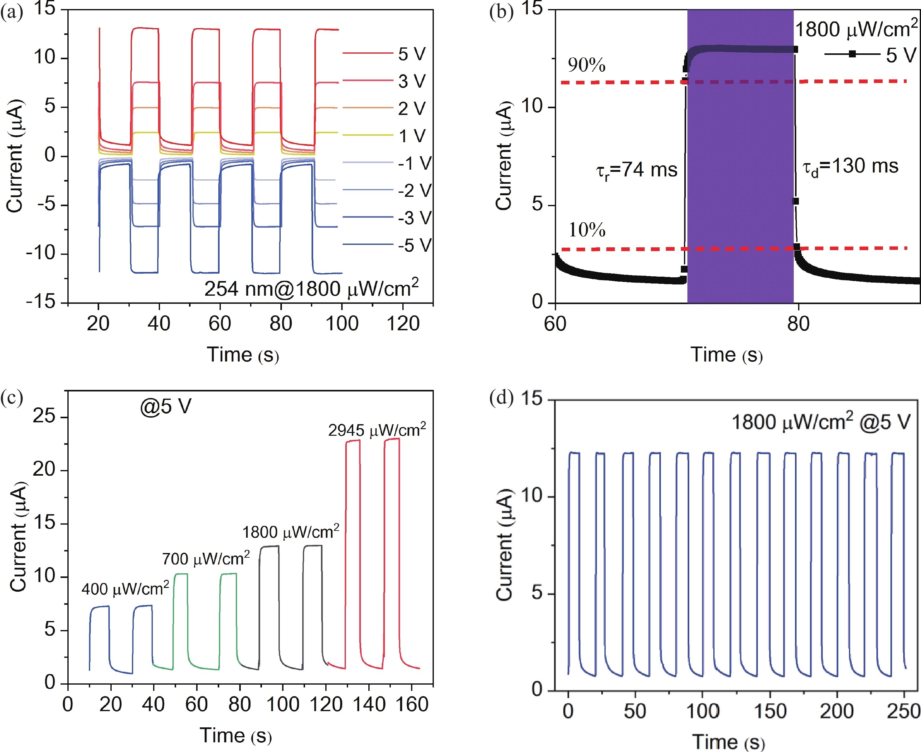
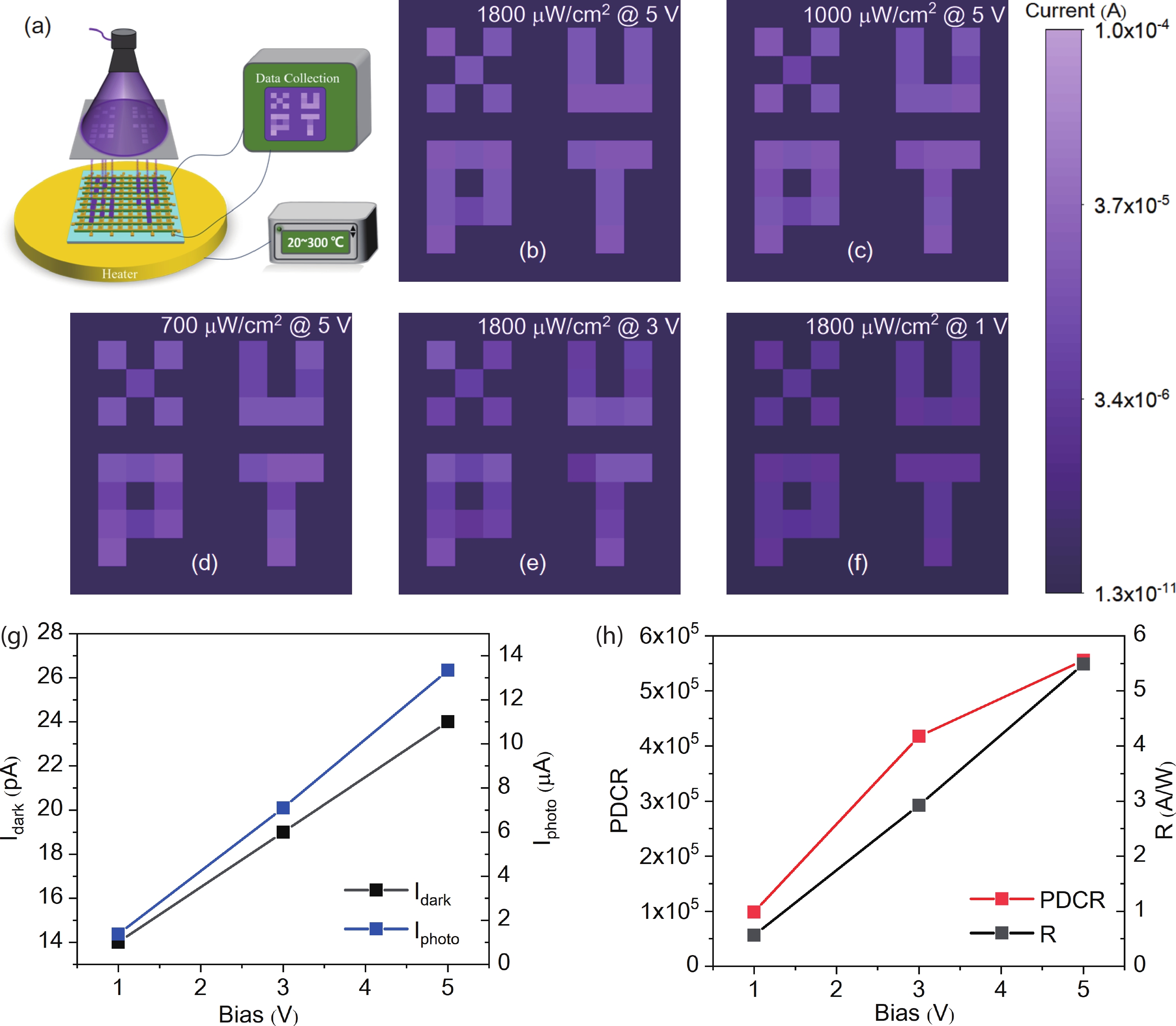
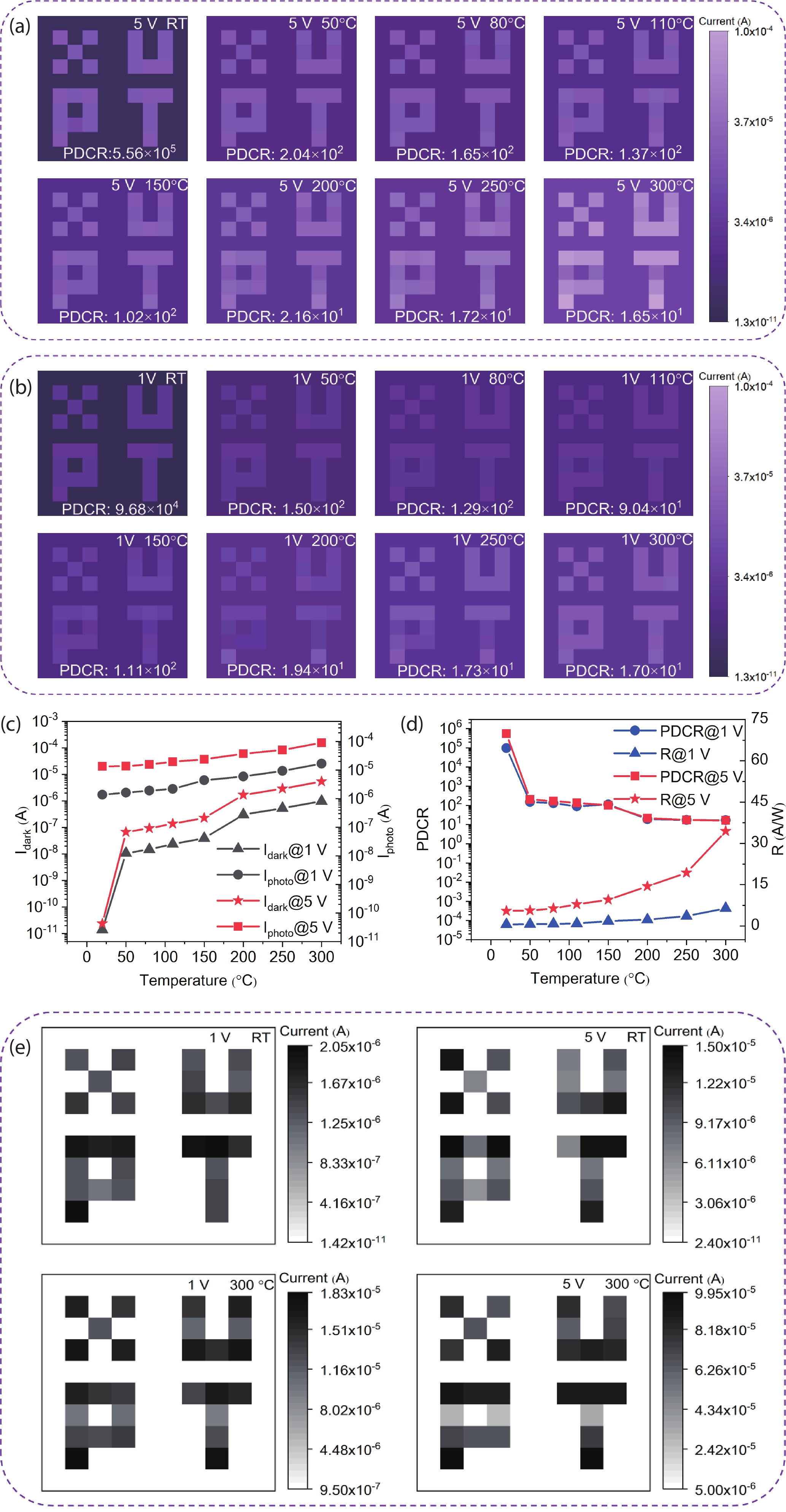
Table 1. Comparison of the performance parameters of the photodetectors at RT.
| Structure | Array | Metal layer number | Bias (V) |
Idark (A) | PDCR | R (A/W) |
EQE (%) |
D* (Jones) |
τr /τd | Ref. |
| β-Ga2O3/sapphire MSM | No | 1 | 20 | 7 × 10⁻¹⁰ | ~105 | 22000 | 1.07 × 10⁷ | 1.1 × 10¹⁶ | / | [31] |
| α-Ga2O3/ZnO heterojunction | No | 1 | 20 | 2.17 × 10⁻⁹ | 21 521 | 2.49 | / | 1.98 × 10¹⁴ | 147 ns | [15] |
| β-Ga2O3/sapphire MSM | No | 1 | 20 | 1.4 × 10⁻¹¹ | 105 | 150 | 7.4 × 10⁴ | / | 1.3 s | [32] |
| β-Ga2O3/sapphire MSM | No | 1 | 15 | / | 9.3 × 10⁴ | 1.26 | 616 | 2.5 × 10¹² | 0.58 s/0.06 s | [33] |
| β-Ga2O3/sapphire MSM | No | 1 | 10 | 1.06 × 10⁻¹¹ | 1.6 × 10³ | 18.23 | / | / | 0.062 s/0.05 s | [34] |
| β-Ga2O3/sapphire MSM | No | 1 | 5 | 2.19 × 10⁻⁸ | 9.43 | 1.45 | / | / | 0.58 s/1.2 s | [35] |
| β-Ga2O3/SiO2/Si MSM | 8 × 8 | 1 | 10 | 6.2 × 10⁻¹³ | 6.13 × 10⁴ | 0.72 | / | 4.18 × 10¹¹ | 1.1 s/0.03 s | [18] |
| β-Ga2O3/sapphire MSM | 4 × 4 | 1 | 10 | 4.0 × 10⁻¹⁰ | 105 | 12.4 (45 V) |
6006 (45 V) |
1.9 × 10¹² | / | [36] |
| β-Ga2O3/sapphire MSM | 4 × 4 | 1 | 5 | 10−11 | 105 | 0.893 | 444 | / | 305 ms/251 ms | [37] |
| β-Ga2O3/sapphire MSM | 4 × 5 | 1 | 10 | / | 2.78 × 10⁵ | 459.38 | 2.24 × 10⁵ | 1.33 × 10¹⁵ | 1.149 s/0.45 s | [38] |
| Al/Al2O3/Ga2O3 | 7 × 7 | 1 | 10 | 1.6 × 10⁻¹¹ | 102 | 295 | 1.4 × 10⁵ | 1.7 × 10¹⁵ | 1.7 s/26.8 s | [39] |
| α-Ga2O3/PET MSM | 3D | 1 | 15 | 1.7 × 10⁻¹⁰ | >102 | 8.9 | 4450 | / | / | [40] |
| β-Ga2O3/sapphire MSM | 16 × 16 | 1 | 5 | 10−11 | 3.4 × 10⁵ | 61.3 | 3 × 10⁴ | 5.2 × 10¹⁴ | 3 ms/35 ms (3 V) |
[23] |
| β-Ga2O3/sapphire MSM | 10 × 10 | 2 | 3 | 1.85 × 10⁻¹¹ | 5.5 × 10⁵ | 4.28 | 2.1 × 10³ | 1.5 × 10¹⁴ | 100 ms/150 ms | This work |
| 5 | 2.4 × 10⁻¹¹ | 5.6 × 10⁵ | 5.5 | 2.7 × 10³ | 2.3 × 10¹⁴ | 74 ms/130 ms |
 DownLoad: CSV
Table 2. Comparison of the performance parameters of the photodetectors at high temperature.
| Structure | Metal layer number |
Bias (V) | Idark (A) | PDCR | R (A/W) | Operating temperature (°C) |
Ref. |
| β-Ga2O3/sapphire MSM | 1 | 20 | ≤10−10 | ≥97 | ~10−2 | 200 | [41] |
| β-Ga2O3/sapphire MSM | 1 | 10 | 6.7 × 10⁻⁹ | ~10 | / | 200 | [42] |
| α-GaOx/sapphire MSM | 1 | 12 | ~10−10 | 7.1 × 10³ | 8 | 280 | [22] |
| β-Ga2O3/sapphire MSM | 1 | 10 | >10−6 | 2.3 | 0.74 | 250 | [43] |
| β-Ga2O3/sapphire MSM | 2 | 5 | 5.4 × 10⁻⁶ | 1.65 × 101 | 34.4 | 300 | This work |
| 1 | 9.82 × 10⁻⁷ | 1.70 × 101 | 6.45 | 300 |
DownLoad: CSV
| [1] |
Liang H L, Han Z Y, Mei Z X. Recent progress of deep ultraviolet photodetectors using amorphous gallium oxide thin films. Phys Status Solidi A, 2021, 218, 2000339 doi: 10.1002/pssa.202000339
|
| [2] |
Xu J J, Zheng W, Huang F. Gallium oxide solar-blind ultraviolet photodetectors: A review. J Mater Chem C, 2019, 7, 8753 doi: 10.1039/C9TC02055A
|
| [3] |
Wei T C, Tsai D S, Ravadgar P, et al. See-through Ga2O3 solar-blind photodetectors for use in harsh environments. IEEE J Sel Top Quantum Electron, 2014, 20, 112 doi: 10.1109/JSTQE.2014.2321517
|
| [4] |
Yang G, Jang S, Ren F, et al. Influence of high-energy proton irradiation on β-Ga2O3 nanobelt field-effect transistors. ACS Appl Mater Interfaces, 2017, 9, 40471 doi: 10.1021/acsami.7b13881
|
| [5] |
Higashiwaki M, Sasaki K, Kuramata A, et al. Gallium oxide (Ga2O3) metal-semiconductor field-effect transistors on single-crystal β-Ga2O3 (010) substrates. Appl Phys Lett, 2012, 100, 013504 doi: 10.1063/1.3674287
|
| [6] |
Kaur D, Vashishtha P, Khan S A, et al. Phase dependent radiation hardness and performance analysis of amorphous and polycrystalline Ga2O3 solar-blind photodetector against swift heavy ion irradiation. J Appl Phys, 2020, 128, 065902 doi: 10.1063/5.0019786
|
| [7] |
Pearton S J, Yang J C, Cary P H, et al. A review of Ga2O3 materials, processing, and devices. Appl Phys Rev, 2018, 5, 011301 doi: 10.1063/1.5006941
|
| [8] |
Roy R, Hill V G, Osborn E F. Polymorphism of Ga2O3 and the system Ga2O3−H2O. J Am Chem Soc, 1952, 74, 719 doi: 10.1021/ja01123a039
|
| [9] |
Orita M, Ohta H, Hirano M, et al. Deep-ultraviolet transparent conductive β-Ga2O3 thin films. Appl Phys Lett, 2000, 77, 4166 doi: 10.1063/1.1330559
|
| [10] |
Kaur D, Kumar M. A strategic review on gallium oxide based deep-ultraviolet photodetectors: Recent progress and future prospects. Adv opt mater, 2021, 9, 2002160 doi: 10.1002/adom.202002160
|
| [11] |
Qian L X, Gu Z, Huang X, et al. Comprehensively improved performance of β-Ga2O3 solar-blind photodetector enabled by a homojunction with unique passivation mechanisms. ACS Appl Mater Interfaces, 2021, 13, 40837 doi: 10.1021/acsami.1c12615
|
| [12] |
Liu Z, Zhi Y S, Zhang S H, et al. Ultrahigh-performance planar β-Ga2O3 solar-blind Schottky photodiode detectors. Sci China Technol Sci, 2021, 64, 59 doi: 10.1007/s11431-020-1701-2
|
| [13] |
Wu D, Zhao Z H, Lu W, et al. Highly sensitive solar-blind deep ultraviolet photodetector based on graphene/PtSe2/β-Ga2O3 2D/3D Schottky junction with ultrafast speed. Nano Res, 2021, 14, 1973 doi: 10.1007/s12274-021-3346-7
|
| [14] |
Qin Y, Sun H D, Long S B, et al. High-performance metal-organic chemical vapor deposition grown ε-Ga2O3 solar-blind photodetector with asymmetric Schottky electrodes. IEEE Electron Device Lett, 2019, 40, 1475 doi: 10.1109/LED.2019.2932382
|
| [15] |
Wang H, Ma J, Cong L, et al. Piezoelectric effect enhanced flexible UV photodetector based on Ga2O3/ZnO heterojunction. Mater Today Phys, 2021, 20, 100464 doi: 10.1016/j.mtphys.2021.100464
|
| [16] |
Wu C, He H L, Hu H Z, et al. Self-healing wearable self-powered deep ultraviolet photodetectors based on Ga2O3. J Semicond, 2023, 44, 072807 doi: 10.1088/1674-4926/44/7/072807
|
| [17] |
Qu Y Y, Wu Z P, Ai M L, et al. Enhanced Ga2O3/SiC ultraviolet photodetector with graphene top electrodes. J Alloys Compd, 2016, 680, 247 doi: 10.1016/j.jallcom.2016.04.134
|
| [18] |
Xie C, Lu X T, Liang Y, et al. Patterned growth of β-Ga2O3 thin films for solar-blind deep-ultraviolet photodetectors array and optical imaging application. J Mater Sci Technol, 2021, 72, 189 doi: 10.1016/j.jmst.2020.09.015
|
| [19] |
Liu Z, Zhi Y S, Zhang M L, et al. A 4 × 4 metal-semiconductor-metal rectangular deep-ultraviolet detector array of Ga2O3 photoconductor with high photo response. Chinese Phys B, 2022, 31, 088503 doi: 10.1088/1674-1056/ac597d
|
| [20] |
Ding M F, Liang K, Yu S J, et al. Aqueous-printed Ga2O3 films for high-performance flexible and heat-resistant deep ultraviolet photodetector and array. Adv Opt Mater, 2022, 10, 2200512 doi: 10.1002/adom.202200512
|
| [21] |
Shen G H, Liu Z, Tang K, et al. High responsivity and fast response 8 × 8 β-Ga2O3 solar-blind ultraviolet imaging photodetector array. Sci China Technol Sci, 2023, 66, 3259 doi: 10.1007/s11431-022-2404-8
|
| [22] |
Hou X H, Zhao X L, Zhang Y, et al. High-performance harsh-environment-resistant GaOx solar-blind photodetectors via defect and doping engineering. Adv Mater, 2022, 34, 2106923 doi: 10.1002/adma.202106923
|
| [23] |
Shen G H, Liu Z, Tan C K, et al. Solar-blind UV communication based on sensitive β-Ga2O3 photoconductive detector array. Appl Phys Lett, 2023, 123, 041103 doi: 10.1063/5.0161521
|
| [24] |
Prabakar K, Venkatachalam S, Jeyachandran Y L, et al. Microstructure, Raman and optical studies on Cd0.6Zn0. 4Te thin films. Mater Sci Eng B, 2004, 107, 99 doi: 10.1016/j.mseb.2003.10.017
|
| [25] |
Zheng W, Huang F, Zheng R S, et al. Low-dimensional structure vacuum-ultraviolet-sensitive (λ < 200 nm) photodetector with fast-response speed based on high-quality AlN micro/nanowire. Adv Mater, 2015, 27, 3921 doi: 10.1002/adma.201500268
|
| [26] |
Shen G H, Liu Z, Zhang M L, et al. 16 × 16 solar-blind UV detector based on β-Ga2O3 sensors. IEEE Electron Device Lett, 2023, 44, 1140 doi: 10.1109/LED.2023.3272909
|
| [27] |
Qin Y, Li L H, Zhao X L, et al. Metal-semiconductor-metal ε-Ga2O3 solar-blind photodetectors with a record-high responsivity rejection ratio and their gain mechanism. Acs Photonics, 2020, 7, 812 doi: 10.1021/acsphotonics.9b01727
|
| [28] |
Hou X H, Zou Y N, Ding M F, et al. Review of polymorphous Ga2O3 materials and their solar-blind photodetector applications. J Phys D: Appl Phys, 2020, 54, 043001 doi: 10.1088/1361-6463/abbb45
|
| [29] |
Zhang Q Y, Li N, Zhang T, et al. Enhanced gain and detectivity of unipolar barrier solar blind avalanche photodetector via lattice and band engineering. Nat commun, 2023, 14, 418 doi: 10.1038/s41467-023-36117-8
|
| [30] |
He H L, Wu C, Hu H Z, et al. Bandgap engineering and oxygen vacancy defect electroactivity inhibition in highly crystalline N-alloyed Ga2O3 films through plasma-enhanced technology. J Phys Chem Lett, 2023, 14, 6444 doi: 10.1021/acs.jpclett.3c01368
|
| [31] |
Xu Y, Cheng Y L, Li Z, et al. Ultrahigh-performance solar-blind photodetectors based on high quality heteroepitaxial single crystalline β-Ga2O3 film grown by vacuumfree, low-cost mist chemical vapor deposition. Adv Mater Technol, 2021, 6, 2001296 doi: 10.1002/admt.202001296
|
| [32] |
Xu Y, An Z Y, Zhang L X, et al. Solar blind deep ultraviolet β-Ga2O3 photodetectors grown on sapphire by the Mist-CVD method. Opt Mater Express, 2018, 8, 2941 doi: 10.1364/OME.8.002941
|
| [33] |
Hu Z G, Cheng Q, Zhang T, et al. Solar-blind photodetectors fabricated on β-Ga2O3 films deposited on 6° off-angled sapphire substrates. J Lumin, 2023, 255, 119596 doi: 10.1016/j.jlumin.2022.119596
|
| [34] |
Wang Q L, Chen J, Huang P, et al. Influence of growth temperature on the characteristics of β-Ga2O3 epitaxial films and related solar-blind photodetectors. Appl Surf Sci, 2019, 489, 101 doi: 10.1016/j.apsusc.2019.05.328
|
| [35] |
Oh S, Jung Y, Mastro M A, et al. Development of solar-blind photodetectors based on Si-implanted β-Ga2O3. Opt Express, 2015, 23, 28300 doi: 10.1364/OE.23.028300
|
| [36] |
Chen Y C, Lu Y J, Liu Q, et al. Ga2O3 photodetector arrays for solar-blind imaging. J Mater Chem C, 2019, 7, 2557 doi: 10.1039/C8TC05251D
|
| [37] |
Peng Y K, Zhang Y, Chen Z W, et al. Arrays of solar-blind ultraviolet photodetector based on β-Ga2O3 epitaxial thin films. IEEE Photonics Technol Lett, 2018, 30, 993 doi: 10.1109/LPT.2018.2826560
|
| [38] |
Zheng Q Q, Chen L R, Li X D, et al. Boosting the performance of deep-ultraviolet photodetector arrays based on phase-transformed heteroepitaxial β-Ga2O3 films for solar-blind imaging. Sci China Technol Sci, 2023, 66, 2707 doi: 10.1007/s11431-023-2416-6
|
| [39] |
Chen Y C, Yang X, Zhang Y, et al. Ultra-sensitive flexible Ga2O3 solar-blind photodetector array realized via ultra-thin absorbing medium. Nano Res, 2021, 15, 3711 doi: 10.1007/s12274-021-3942-6
|
| [40] |
Chen Y, Lu Y J, Liao M Y, et al. 3D solar-blind Ga2O3 photodetector array realized via origami method. Adv Funct Mater, 2019, 29, 1906040 doi: 10.1002/adfm.201906040
|
| [41] |
Zhou H T, Cong L J, Ma J G, et al. High-performance high-temperature solar-blind photodetector based on polycrystalline Ga2O3 film. J Alloys Compd, 2020, 847, 156536 doi: 10.1016/j.jallcom.2020.156536
|
| [42] |
Xu Y, Chen X, Zhou D, et al. Carrier transport and gain mechanisms in β-Ga2O3-based metal-semiconductor-metal solar-blind Schottky photodetectors. IEEE Trans Electron Devices, 2019, 66, 2276 doi: 10.1109/TED.2019.2906906
|
| [43] |
Tak B R, Garg M, Dewan S, et al. High-temperature photocurrent mechanism of β-Ga2O3 based metal-semiconductor-metal solar-blind photodetectors. J Appl Phys, 2019, 125, 144501 doi: 10.1063/1.5088532
|


Article views: 2830 Times PDF downloads: 235 Times Cited by: 0 Times
Received: 06 March 2024 Revised: 16 May 2024 Online: Accepted Manuscript: 04 June 2024Uncorrected proof: 04 June 2024Published: 15 September 2024
| Citation: |
Haifeng Chen, Zhanhang Liu, Yixin Zhang, Feilong Jia, Chenlu Wu, Qin Lu, Xiangtai Liu, Shaoqing Wang. 10 × 10 Ga2O3-based solar-blind UV detector array and imaging characteristic[J]. Journal of Semiconductors, 2024, 45(9): 092502. doi: 10.1088/1674-4926/24030005
****
H F Chen, Z H Liu, Y X Zhang, F L Jia, C L Wu, Q Lu, X T Liu, and S Q Wang, 10 × 10 Ga2O3-based solar-blind UV detector array and imaging characteristic[J]. J. Semicond., 2024, 45(9), 092502 doi: 10.1088/1674-4926/24030005

|
 Haifeng Chen received the Ph.D. degree from Xidian University in 2008. He is currently a Professor at Xi’an University of Posts and Telecommunications. His research interests focus on Ga2O3 material and devices
 Zhanhang Liu received her BS degree from Xi’an University of Posts and Telecommunications in 2022. She is currently a Master’s student at Xi’an University of Posts and Telecommunications. Her research focuses on Ga2O3 photodetectors
 Yixin Zhang received her BS degree from Xianmen University of Technology in 2023. She is currently a Master's student at Xi'an University of Posts and Telecommunications. Her research focuses on Ga2O3 devices
| [1] |
Liang H L, Han Z Y, Mei Z X. Recent progress of deep ultraviolet photodetectors using amorphous gallium oxide thin films. Phys Status Solidi A, 2021, 218, 2000339 doi: 10.1002/pssa.202000339
|
| [2] |
Xu J J, Zheng W, Huang F. Gallium oxide solar-blind ultraviolet photodetectors: A review. J Mater Chem C, 2019, 7, 8753 doi: 10.1039/C9TC02055A
|
| [3] |
Wei T C, Tsai D S, Ravadgar P, et al. See-through Ga2O3 solar-blind photodetectors for use in harsh environments. IEEE J Sel Top Quantum Electron, 2014, 20, 112 doi: 10.1109/JSTQE.2014.2321517
|
| [4] |
Yang G, Jang S, Ren F, et al. Influence of high-energy proton irradiation on β-Ga2O3 nanobelt field-effect transistors. ACS Appl Mater Interfaces, 2017, 9, 40471 doi: 10.1021/acsami.7b13881
|
| [5] |
Higashiwaki M, Sasaki K, Kuramata A, et al. Gallium oxide (Ga2O3) metal-semiconductor field-effect transistors on single-crystal β-Ga2O3 (010) substrates. Appl Phys Lett, 2012, 100, 013504 doi: 10.1063/1.3674287
|
| [6] |
Kaur D, Vashishtha P, Khan S A, et al. Phase dependent radiation hardness and performance analysis of amorphous and polycrystalline Ga2O3 solar-blind photodetector against swift heavy ion irradiation. J Appl Phys, 2020, 128, 065902 doi: 10.1063/5.0019786
|
| [7] |
Pearton S J, Yang J C, Cary P H, et al. A review of Ga2O3 materials, processing, and devices. Appl Phys Rev, 2018, 5, 011301 doi: 10.1063/1.5006941
|
| [8] |
Roy R, Hill V G, Osborn E F. Polymorphism of Ga2O3 and the system Ga2O3−H2O. J Am Chem Soc, 1952, 74, 719 doi: 10.1021/ja01123a039
|
| [9] |
Orita M, Ohta H, Hirano M, et al. Deep-ultraviolet transparent conductive β-Ga2O3 thin films. Appl Phys Lett, 2000, 77, 4166 doi: 10.1063/1.1330559
|
| [10] |
Kaur D, Kumar M. A strategic review on gallium oxide based deep-ultraviolet photodetectors: Recent progress and future prospects. Adv opt mater, 2021, 9, 2002160 doi: 10.1002/adom.202002160
|
| [11] |
Qian L X, Gu Z, Huang X, et al. Comprehensively improved performance of β-Ga2O3 solar-blind photodetector enabled by a homojunction with unique passivation mechanisms. ACS Appl Mater Interfaces, 2021, 13, 40837 doi: 10.1021/acsami.1c12615
|
| [12] |
Liu Z, Zhi Y S, Zhang S H, et al. Ultrahigh-performance planar β-Ga2O3 solar-blind Schottky photodiode detectors. Sci China Technol Sci, 2021, 64, 59 doi: 10.1007/s11431-020-1701-2
|
| [13] |
Wu D, Zhao Z H, Lu W, et al. Highly sensitive solar-blind deep ultraviolet photodetector based on graphene/PtSe2/β-Ga2O3 2D/3D Schottky junction with ultrafast speed. Nano Res, 2021, 14, 1973 doi: 10.1007/s12274-021-3346-7
|
| [14] |
Qin Y, Sun H D, Long S B, et al. High-performance metal-organic chemical vapor deposition grown ε-Ga2O3 solar-blind photodetector with asymmetric Schottky electrodes. IEEE Electron Device Lett, 2019, 40, 1475 doi: 10.1109/LED.2019.2932382
|
| [15] |
Wang H, Ma J, Cong L, et al. Piezoelectric effect enhanced flexible UV photodetector based on Ga2O3/ZnO heterojunction. Mater Today Phys, 2021, 20, 100464 doi: 10.1016/j.mtphys.2021.100464
|
| [16] |
Wu C, He H L, Hu H Z, et al. Self-healing wearable self-powered deep ultraviolet photodetectors based on Ga2O3. J Semicond, 2023, 44, 072807 doi: 10.1088/1674-4926/44/7/072807
|
| [17] |
Qu Y Y, Wu Z P, Ai M L, et al. Enhanced Ga2O3/SiC ultraviolet photodetector with graphene top electrodes. J Alloys Compd, 2016, 680, 247 doi: 10.1016/j.jallcom.2016.04.134
|
| [18] |
Xie C, Lu X T, Liang Y, et al. Patterned growth of β-Ga2O3 thin films for solar-blind deep-ultraviolet photodetectors array and optical imaging application. J Mater Sci Technol, 2021, 72, 189 doi: 10.1016/j.jmst.2020.09.015
|
| [19] |
Liu Z, Zhi Y S, Zhang M L, et al. A 4 × 4 metal-semiconductor-metal rectangular deep-ultraviolet detector array of Ga2O3 photoconductor with high photo response. Chinese Phys B, 2022, 31, 088503 doi: 10.1088/1674-1056/ac597d
|
| [20] |
Ding M F, Liang K, Yu S J, et al. Aqueous-printed Ga2O3 films for high-performance flexible and heat-resistant deep ultraviolet photodetector and array. Adv Opt Mater, 2022, 10, 2200512 doi: 10.1002/adom.202200512
|
| [21] |
Shen G H, Liu Z, Tang K, et al. High responsivity and fast response 8 × 8 β-Ga2O3 solar-blind ultraviolet imaging photodetector array. Sci China Technol Sci, 2023, 66, 3259 doi: 10.1007/s11431-022-2404-8
|
| [22] |
Hou X H, Zhao X L, Zhang Y, et al. High-performance harsh-environment-resistant GaOx solar-blind photodetectors via defect and doping engineering. Adv Mater, 2022, 34, 2106923 doi: 10.1002/adma.202106923
|
| [23] |
Shen G H, Liu Z, Tan C K, et al. Solar-blind UV communication based on sensitive β-Ga2O3 photoconductive detector array. Appl Phys Lett, 2023, 123, 041103 doi: 10.1063/5.0161521
|
| [24] |
Prabakar K, Venkatachalam S, Jeyachandran Y L, et al. Microstructure, Raman and optical studies on Cd0.6Zn0. 4Te thin films. Mater Sci Eng B, 2004, 107, 99 doi: 10.1016/j.mseb.2003.10.017
|
| [25] |
Zheng W, Huang F, Zheng R S, et al. Low-dimensional structure vacuum-ultraviolet-sensitive (λ < 200 nm) photodetector with fast-response speed based on high-quality AlN micro/nanowire. Adv Mater, 2015, 27, 3921 doi: 10.1002/adma.201500268
|
| [26] |
Shen G H, Liu Z, Zhang M L, et al. 16 × 16 solar-blind UV detector based on β-Ga2O3 sensors. IEEE Electron Device Lett, 2023, 44, 1140 doi: 10.1109/LED.2023.3272909
|
| [27] |
Qin Y, Li L H, Zhao X L, et al. Metal-semiconductor-metal ε-Ga2O3 solar-blind photodetectors with a record-high responsivity rejection ratio and their gain mechanism. Acs Photonics, 2020, 7, 812 doi: 10.1021/acsphotonics.9b01727
|
| [28] |
Hou X H, Zou Y N, Ding M F, et al. Review of polymorphous Ga2O3 materials and their solar-blind photodetector applications. J Phys D: Appl Phys, 2020, 54, 043001 doi: 10.1088/1361-6463/abbb45
|
| [29] |
Zhang Q Y, Li N, Zhang T, et al. Enhanced gain and detectivity of unipolar barrier solar blind avalanche photodetector via lattice and band engineering. Nat commun, 2023, 14, 418 doi: 10.1038/s41467-023-36117-8
|
| [30] |
He H L, Wu C, Hu H Z, et al. Bandgap engineering and oxygen vacancy defect electroactivity inhibition in highly crystalline N-alloyed Ga2O3 films through plasma-enhanced technology. J Phys Chem Lett, 2023, 14, 6444 doi: 10.1021/acs.jpclett.3c01368
|
| [31] |
Xu Y, Cheng Y L, Li Z, et al. Ultrahigh-performance solar-blind photodetectors based on high quality heteroepitaxial single crystalline β-Ga2O3 film grown by vacuumfree, low-cost mist chemical vapor deposition. Adv Mater Technol, 2021, 6, 2001296 doi: 10.1002/admt.202001296
|
| [32] |
Xu Y, An Z Y, Zhang L X, et al. Solar blind deep ultraviolet β-Ga2O3 photodetectors grown on sapphire by the Mist-CVD method. Opt Mater Express, 2018, 8, 2941 doi: 10.1364/OME.8.002941
|
| [33] |
Hu Z G, Cheng Q, Zhang T, et al. Solar-blind photodetectors fabricated on β-Ga2O3 films deposited on 6° off-angled sapphire substrates. J Lumin, 2023, 255, 119596 doi: 10.1016/j.jlumin.2022.119596
|
| [34] |
Wang Q L, Chen J, Huang P, et al. Influence of growth temperature on the characteristics of β-Ga2O3 epitaxial films and related solar-blind photodetectors. Appl Surf Sci, 2019, 489, 101 doi: 10.1016/j.apsusc.2019.05.328
|
| [35] |
Oh S, Jung Y, Mastro M A, et al. Development of solar-blind photodetectors based on Si-implanted β-Ga2O3. Opt Express, 2015, 23, 28300 doi: 10.1364/OE.23.028300
|
| [36] |
Chen Y C, Lu Y J, Liu Q, et al. Ga2O3 photodetector arrays for solar-blind imaging. J Mater Chem C, 2019, 7, 2557 doi: 10.1039/C8TC05251D
|
| [37] |
Peng Y K, Zhang Y, Chen Z W, et al. Arrays of solar-blind ultraviolet photodetector based on β-Ga2O3 epitaxial thin films. IEEE Photonics Technol Lett, 2018, 30, 993 doi: 10.1109/LPT.2018.2826560
|
| [38] |
Zheng Q Q, Chen L R, Li X D, et al. Boosting the performance of deep-ultraviolet photodetector arrays based on phase-transformed heteroepitaxial β-Ga2O3 films for solar-blind imaging. Sci China Technol Sci, 2023, 66, 2707 doi: 10.1007/s11431-023-2416-6
|
| [39] |
Chen Y C, Yang X, Zhang Y, et al. Ultra-sensitive flexible Ga2O3 solar-blind photodetector array realized via ultra-thin absorbing medium. Nano Res, 2021, 15, 3711 doi: 10.1007/s12274-021-3942-6
|
| [40] |
Chen Y, Lu Y J, Liao M Y, et al. 3D solar-blind Ga2O3 photodetector array realized via origami method. Adv Funct Mater, 2019, 29, 1906040 doi: 10.1002/adfm.201906040
|
| [41] |
Zhou H T, Cong L J, Ma J G, et al. High-performance high-temperature solar-blind photodetector based on polycrystalline Ga2O3 film. J Alloys Compd, 2020, 847, 156536 doi: 10.1016/j.jallcom.2020.156536
|
| [42] |
Xu Y, Chen X, Zhou D, et al. Carrier transport and gain mechanisms in β-Ga2O3-based metal-semiconductor-metal solar-blind Schottky photodetectors. IEEE Trans Electron Devices, 2019, 66, 2276 doi: 10.1109/TED.2019.2906906
|
| [43] |
Tak B R, Garg M, Dewan S, et al. High-temperature photocurrent mechanism of β-Ga2O3 based metal-semiconductor-metal solar-blind photodetectors. J Appl Phys, 2019, 125, 144501 doi: 10.1063/1.5088532
|

 WeChat ID
Journal of Semiconductors © 2017 All Rights Reserved 京ICP备05085259号-2


