J. Semicond. > 2024, Volume 45 > Issue 9 > 091101

REVIEWS

Recent progress on fabrication, spectroscopy properties, and device applications in Sn-doped CdS micro-nano structures

Bo Cao1, 2, Ye Tian1, 2, , Huan Fei Wen1, 2, , Hao Guo1, 2, Xiaoyu Wu3, , Liangjie Li1, 2, Zhenrong Zhang1, 2, Lai Liu1, 2, Qiang Zhu1, 2, Jun Tang1, 2, and Jun Liu1, 2,

+ Author Affiliations

 Corresponding author: Ye Tian, tianye080t@163.com; Huan Fei Wen, wenhuanfei@nuc.edu.cn; Xiaoyu Wu, Xymems@stu.xjtu.edu.cn; Jun Tang, tangjun@nuc.edu.cn; Jun Liu, liuj@nuc.edu.cn

DOI: 10.1088/1674-4926/24040041

PDF

Turn off MathJax

Abstract: One-dimensional semiconductor materials possess excellent photoelectric properties and potential for the construction of integrated nanodevices. Among them, Sn-doped CdS has different micro-nano structures, including nanoribbons, nanowires, comb-like structures, and superlattices, with rich optical microcavity modes, excellent optical properties, and a wide range of application fields. This article reviews the research progress of various micrometer structures of Sn-doped CdS, systematically elaborates the effects of different growth conditions on the preparation of Sn-doped CdS micro-nano structures, as well as the spectral characteristics of these structures and their potential applications in certain fields. With the continuous progress of nanotechnology, it is expected that Sn-doped CdS micro-nano structures will achieve more breakthroughs in the field of optoelectronics and form cross-integration with other fields, jointly promoting scientific, technological, and social development.

Key words: Sn-doped CdSmicro-nano structuresuperlatticesoptical microcavity


[1]
Cavin R K, Lugli P, Zhirnov V V. Science and engineering beyond Moore’s law. Proc IEEE, 2012, 100, 1720 doi: 10.1109/JPROC.2012.2190155
[2]
Haensch W, Nowak E J, Dennard R H, et al. Silicon CMOS devices beyond scaling. IBM J Res Dev, 2006, 50, 339 doi: 10.1147/rd.504.0339
[3]
Ye Y, Dai Y, Dai L, et al. High-performance single CdS nanowire (nanobelt) Schottky junction solar cells with Au/graphene Schottky electrodes. ACS Appl Mater Interfaces, 2010, 2, 3406 doi: 10.1021/am1007672
[4]
Jia C C, Lin Z Y, Huang Y, et al. Nanowire electronics: From nanoscale to macroscale. Chem Rev, 2019, 119, 9074 doi: 10.1021/acs.chemrev.9b00164
[5]
Yan R X, Gargas D, Yang P D. Nanowire photonics. Nature Photon, 2009, 3, 569 doi: 10.1038/nphoton.2009.184
[6]
Quan L N, Kang J, Ning C Z, et al. Nanowires for photonics. Chem Rev, 2019, 119, 9153 doi: 10.1021/acs.chemrev.9b00240
[7]
Chen C H, Chang S J, Chang S P, et al. Novel fabrication of UV photodetector based on ZnO nanowire/p-GaN heterojunction. Chem Phys Lett, 2009, 476, 69 doi: 10.1016/j.cplett.2009.06.007
[8]
Yang Z Y, Albrow-Owen T, Cui H, et al. Single-nanowire spectrometers. Science, 2019, 365, 1017 doi: 10.1126/science.aax8814
[9]
Zhang M, Wille M, Röder R, et al. Amphoteric nature of Sn in CdS nanowires. Nano Lett, 2014, 14, 518 doi: 10.1021/nl4035169
[10]
Granados del Águila A, Jha B, Pietra F, et al. Observation of the full exciton and phonon fine structure in CdSe/CdS dot-in-rod heteronanocrystals. ACS Nano, 2014, 8, 5921 doi: 10.1021/nn501026t
[11]
Scott R, Prudnikau A V, Antanovich A, et al. A comparative study demonstrates strong size tunability of carrier–phonon coupling in CdSe-based 2D and 0D nanocrystals. Nanoscale, 2019, 11, 3958 doi: 10.1039/C8NR09458F
[12]
Achtstein A W, Schliwa A, Prudnikau A, et al. Electronic structure and exciton–phonon interaction in two-dimensional colloidal CdSe nanosheets. Nano Lett, 2012, 12, 3151 doi: 10.1021/nl301071n
[13]
Achermann M, Bartko A P, Hollingsworth J A, et al. The effect of Auger heating on intraband carrier relaxation in semiconductor quantum rods. Nat Phys, 2006, 2, 557 doi: 10.1038/nphys363
[14]
Klimov V I. Optical nonlinearities and ultrafast carrier dynamics in semiconductor nanocrystals. J Phys Chem B, 2000, 104, 6112 doi: 10.1021/jp9944132
[15]
Hou X Q, Kang J, Qin H Y, et al. Engineering Auger recombination in colloidal quantum dots via dielectric screening. Nat Commun, 2019, 10, 1750 doi: 10.1038/s41467-019-09737-2
[16]
Wang Y, Sun H D. Advances and prospects of lasers developed from colloidal semiconductor nanostructures. Prog Quant Electron, 2018, 60, 1 doi: 10.1016/j.pquantelec.2018.05.002
[17]
Jang J, Song G, Kyhm K, et al. Optical gain of inelastic exciton-exciton scattering in CdS nanowires. Appl Phys Lett, 2019, 114, 1101 doi: 10.1063/1.5086782
[18]
Zhang Z, Wang Y L, Yin S Y, et al. Exciton-polariton light-emitting diode based on a ZnO microwire. Opt Express, 2017, 25, 17375 doi: 10.1364/OE.25.017375
[19]
Chen J Y, Wong T M, Chang C W, et al. Self-polarized spin-nanolasers. Nature Nanotech, 2014, 9, 845 doi: 10.1038/nnano.2014.195
[20]
Zhao Z, Zhong M Y, Zhou W C, et al. Simultaneous triplet exciton–phonon and exciton–photon photoluminescence in the individual weak confinement CsPbBr3 micro/nanowires. J Phys Chem C, 2019, 123, 25349 doi: 10.1021/acs.jpcc.9b06643
[21]
Takagahara T. Electron−phonon interactions in semiconductor nanocrystals. J Lumin, 1996, 70, 129 doi: 10.1016/0022-2313(96)00050-6
[22]
Zheng Q, Zhou W C, Peng Y H, et al. Surface polarons and optical micro-cavity modulated broad range multi-mode emission of Te-doped CdS nanowires. Nanotechnology, 2018, 29, 465709 doi: 10.1088/1361-6528/aadf64
[23]
Lai Y Y, Lan Y P, Lu T C. Strong light–matter interaction in ZnO microcavities. Light Sci Appl, 2013, 2, e76 doi: 10.1038/lsa.2013.32
[24]
Tawara T, Yoshida H, Yogo T, et al. Microcavities with distributed Bragg reflectors based on ZnSe/MgS superlattice grown by MOVPE. J Cryst Growth, 2000, 221, 699 doi: 10.1016/S0022-0248(00)00803-4
[25]
Claudon J, Bleuse J, Malik N S, et al. A highly efficient single-photon source based on a quantum dot in a photonic nanowire. Nat Photonics, 2010, 4, 174 doi: 10.1038/nphoton.2009.287x
[26]
Mak K F, Shan J. Photonics and optoelectronics of 2D semiconductor transition metal dichalcogenides. Nature Photon, 2016, 10, 216 doi: 10.1038/nphoton.2015.282
[27]
Fang K J, Matheny M H, Luan X S, et al. Optical transduction and routing of microwave phonons in cavity-optomechanical circuits. Nat Photonics, 2016, 10, 489 doi: 10.1038/nphoton.2016.107
[28]
Tochitsky I, Trautman J, Gallerani N, et al. Restoring visual function to the blind retina with a potent, safe and long-lasting photoswitch. Sci Rep, 2017, 7, 45487 doi: 10.1038/srep45487
[29]
van Vugt L K, Rühle S, Ravindran P, et al. Exciton polaritons confined in a ZnO nanowire cavity. Phys Rev Lett, 2006, 97, 147401 doi: 10.1103/PhysRevLett.97.147401
[30]
Stevenson R M, Salter C L, Nilsson J, et al. Indistinguishable entangled photons generated by a light-emitting diode. Phys Rev Lett, 2012, 108, 040503 doi: 10.1103/PhysRevLett.108.040503
[31]
Tian Y, Peng H, Yao S, et al. Repeatedly and superbroad savelength tuning microcavity in a single Sn-doped CdS microcone. J Phys Chem C, 2022, 126, 12696 doi: 10.1021/acs.jpcc.2c04142
[32]
Zhang L, Zhang Y, Guo Y, et al. Growth of CdS nanotubes and their strong optical microcavity effects. Nanoscale, 2019, 11, 5325 doi: 10.1039/C8NR10323B
[33]
Song G L, Guo S, Wang X X, et al. Temperature dependent Raman and photoluminescence of an individual Sn-doped CdS branched nanostructure. New J Phys, 2015, 17, 063024 doi: 10.1088/1367-2630/17/6/063024
[34]
Zhang Q L, Zhu X L, Li Y Y, et al. Nanolaser arrays based on individual waved CdS nanoribbons. Laser Photonics Rev, 2016, 10, 458 doi: 10.1002/lpor.201500268
[35]
Dai G Z, Wan Q, Zhou C J, et al. Sn-catalyst growth and optical waveguide of ultralong CdS nanowires. Chem Phys Lett, 2010, 497, 85 doi: 10.1016/j.cplett.2010.07.095
[36]
Dai B B, Fan C, Xu X, et al. Growing a CdS flag from a wire with in situ control of the catalyst. CrystEngComm, 2021, 23, 3664 doi: 10.1039/D1CE00289A
[37]
Dai G Z, Zou B S, Wang Z L. Preparation and periodic emission of superlattice CdS/CdS: SnS2 microwires. J Am Chem Soc, 2010, 132, 12174 doi: 10.1021/ja1037963
[38]
Dai G Z, Liu R B, Wan Q, et al. Color-tunable periodic spatial emission of alloyed CdS1-xSex/Sn: CdS1-xSex superlattice microwires. Opt Mater Express, 2011, 1, 1185 doi: 10.1364/OME.1.001185
[39]
Zou S Y, Zhou W C, Liu R B, et al. Cavity-enhanced microphotoluminescence in a core–shell n–p CdS/CdO micrometer wire and Its efficient surface photovoltage responses in the whole visible range. J Phys Chem C, 2017, 121, 14349 doi: 10.1021/acs.jpcc.7b04053
[40]
Liu R B, Li Z A, Zhang C H, et al. Single-step synthesis of monolithic comb-like CdS nanostructures with tunable waveguide properties. Nano Lett, 2013, 13, 2997 doi: 10.1021/nl401726z
[41]
Arguello C A, Rousseau D L, Porto S P S. First-order Raman effect in wurtzite-type crystals. Phys Rev, 1969, 181, 1351 doi: 10.1103/PhysRev.181.1351
[42]
Smith A J, Meek P E, Liang W Y. Raman scattering studies of SnS2 and SnSe2. J Phys C Solid State Phys, 1977, 10, 1321 doi: 10.1088/0022-3719/10/8/035
[43]
Zhou W C, Liu R B, Wan Q, et al. Bound exciton and optical properties of SnO2 one-dimensional nanostructures. J Phys Chem C, 2009, 113, 1719 doi: 10.1021/jp808422a
[44]
Abello L, Bochu B, Gaskov A, et al. Structural characterization of nanocrystalline SnO2 by X-ray and Raman spectroscopy. J Solid State Chem, 1998, 135, 78 doi: 10.1006/jssc.1997.7596
[45]
Peng Y H, Luo Y, Zhou W C, et al. Photoluminescence and boosting electron-phonon coupling in CdS nanowires with variable Sn(IV) dopant concentration. Nanoscale Res Lett, 2021, 16, 19 doi: 10.1186/s11671-021-03485-3
[46]
Scott J F, Damen T C, Silfvast W T, et al. Resonant Raman scattering in ZnS and ZnSe with the cadmium laser. Opt Commun, 1970, 1, 397 doi: 10.1016/0030-4018(70)90081-7
[47]
Pan A L, Liu R B, Zou B S. Phonon-assisted stimulated emission from single CdS nanoribbons at room temperature. Appl Phys Lett, 2006, 88, 3102 doi: 10.1063/1.2198089
[48]
Xu J Y, Zhuang X J, Guo P F, et al. Dilute tin-doped CdS nanowires for low-loss optical waveguiding. J Mater Chem C, 2013, 1, 4391 doi: 10.1039/c3tc30492b
[49]
Guo S, Wang L, Ding C J, et al. Tunable optical loss and multi-band photodetection based on tin doped CdS nanowire. J Alloys Compd, 2020, 835, 155330 doi: 10.1016/j.jallcom.2020.155330
[50]
Aguilar-Hern ndez J, Contreras-Puente G, Morales-Acevedo A, et al. Photoluminescence and structural properties of cadmium sulphide thin films grown by different techniques. Semicond Sci Technol, 2003, 18, 111 doi: 10.1088/0268-1242/18/2/308
[51]
Varshni Y P. Temperature dependence of the energy gap in semiconductors. Physica, 1967, 34, 149 doi: 10.1016/0031-8914(67)90062-6
[52]
Zhang L, Liu R B, Zou B S. Sn-doped CdS nanowires with low-temperature lasing by CW-laser excitation. ACS Appl Electron Mater, 2020, 2, 282 doi: 10.1021/acsaelm.9b00766
[53]
Liu B, Chen R, Xu X L, et al. Exciton-related photoluminescence and lasing in CdS nanobelts. J Phys Chem C, 2011, 115, 12826 doi: 10.1021/jp203551f
[54]
Notomi M, Kuramochi E, Tanabe T. Large-scale arrays of ultrahigh-Q coupled nanocavities. Nature Photon, 2008, 2, 741 doi: 10.1038/nphoton.2008.226
[55]
Gou G Y, Dai G Z, Qian C, et al. High-performance ultraviolet photodetectors based on CdS/CdS: SnS2 superlattice nanowires. Nanoscale, 2016, 8, 14580 doi: 10.1039/C6NR02915A
[56]
Tian Y, Zhang Y Y, Peng H, et al. Revealing the quantum-confined free exciton A anisotropic emission in a CdS/CdS: SnS2 superlattice nanocone via angle-resolved photoluminescence spectroscopy. J Phys Chem C, 2022, 126, 1064 doi: 10.1021/acs.jpcc.1c09755
[57]
Tian Y, Yao S F, Lin W C, et al. Effect of quantum confinement on polarization anisotropy emission in Sn-doped CdS microcones. Mater Adv, 2022, 3, 8407 doi: 10.1039/D2MA00883A
[58]
Maslov A V, Ning C Z. Radius-dependent polarization anisotropy in semiconductor nanowires. Phys Rev B, 2005, 72, 161310 doi: 10.1103/PhysRevB.72.161310
[59]
Guo S, Liu R B, Niu C H, et al. Tin nanoparticles–enhanced optical transportation in branched CdS nanowire waveguides. Adv Opt Mater, 2018, 6, 1800305 doi: 10.1002/adom.201800305
[60]
Zhou W C, Tang D S, Liu R B, et al. Structure and optical properties of pure and doped ZnO 1D nanostructures. Mate Lett, 2013, 91, 369 doi: 10.1016/j.matlet.2012.10.041
[61]
Guo S, Zhao F Y, Li Y, et al. Individual dual-emitting CdS multi-branched nanowire arrays under various pumping powers. Appl Phys Lett, 2016, 109, 162101 doi: 10.1063/1.4964879
[62]
Liu R B, Chen Y J, Wang F F, et al. Stimulated emission from trapped excitons in SnO2 nanowires. Physica E Low Dimension Syst Nanostruct, 2007, 39, 223 doi: 10.1016/j.physe.2007.04.009
[63]
Zhang Q L, Liu H W, Guo P F, et al. Vapor growth and interfacial carrier dynamics of high-quality CdS-CdSSe-CdS axial nanowire heterostructures. Nano Energy, 2017, 32, 28 doi: 10.1016/j.nanoen.2016.12.014
[64]
Li L, Yang S M, Han F, et al. Optical sensor based on a single CdS nanobelt. Sensors, 2014, 14, 7332 doi: 10.3390/s140407332
[65]
Zhou W C, Peng Y H, Yin Y L, et al. Broad spectral response photodetector based on individual tin-doped CdS nanowire. AIP Adv, 2014, 4, 3005 doi: 10.1063/1.4897521
[66]
Jie J S, Zhang W J, Jiang Y, et al. Photoconductive characteristics of single-crystal CdS nanoribbons. Nano Leet, 2006, 6, 1887 doi: 10.1021/nl060867g
[67]
Zhou W C, Zhou Y, Peng Y H, et al. Ultrahigh sensitivity and gain white light photodetector based on GaTe/Sn: CdS nanoflake/nanowire heterostructures. Nanotechnology, 2014, 25, 445202 doi: 10.1088/0957-4484/25/44/445202
[68]
Gou G Y, Dai G Z, Wang X W, et al. High-performance and flexible photodetectors based on P3HT/CdS/CdS: SnS2 superlattice nanowires hybrid films. Appl Phys A, 2017, 123, 731 doi: 10.1007/s00339-017-1344-0
[69]
Wang X F, Song W F, Liu B, et al. High-performance organic-inorganic hybrid photodetectors based on P3HT: CdSe nanowire heterojunctions on rigid and flexible substrates. Adv Funct Materials, 2013, 23, 1202 doi: 10.1002/adfm.201201786
[70]
Dai G Z, Zou H Y, Wang X F, et al. Piezo-phototronic effect enhanced responsivity of photon sensor based on composition-tunable ternary CdSxSe1–x nanowires. ACS Photonics, 2017, 4, 2495 doi: 10.1021/acsphotonics.7b00724
[71]
Hao Y, Guo S, Weller D, et al. Position-sensitive array photodetector based on comb-like CdS nanostructure with cone-shape branches. Adv Funct Materials, 2019, 29, 1805967 doi: 10.1002/adfm.201805967
[72]
Pan A L, Zhou W C, Leong E S P, et al. Super-broadly wavelength-tunable semiconductor nanowire lasers on a single substrate. 2009 Conference on Lasers and Electro-Optics and 2009 Conference on Quantum electronics and Laser Science Conference, 2009, 1 doi: 10.1364/CLEO.2009.CTuY7
[73]
Zhang Q L, Wang S W, Liu X X, et al. Low threshold, single-mode laser based on individual CdS nanoribbons in dielectric DBR microcavity. Nano Energy, 2016, 30, 481 doi: 10.1016/j.nanoen.2016.10.045
[74]
Wu Y X, Xiang Y, Zhao S D, et al. Auto-alignment of CdS nanowires via optical tweezers. Appl Phys A, 2022, 128, 200 doi: 10.1007/s00339-022-05350-1
[75]
Guo S, Wang X F, Zhao X Y, et al. The realization of the nanoscale bar-codes based on CdS branched nanostructure. J Alloys Compd, 2023, 969, 172339 doi: 10.1016/j.jallcom.2023.172339
[76]
Zhang J, Jiang F H. Temperature-dependent photoluminescence of Mg-doped CdS nanowires. Phys Lett A, 2009, 373, 3888 doi: 10.1016/j.physleta.2009.08.034
[77]
Zhai T Y, Fang X S, Li L, et al. One-dimensional CdS nanostructures: Synthesis, properties, and applications. Nanoscale, 2010, 2, 168 doi: 10.1039/b9nr00415g
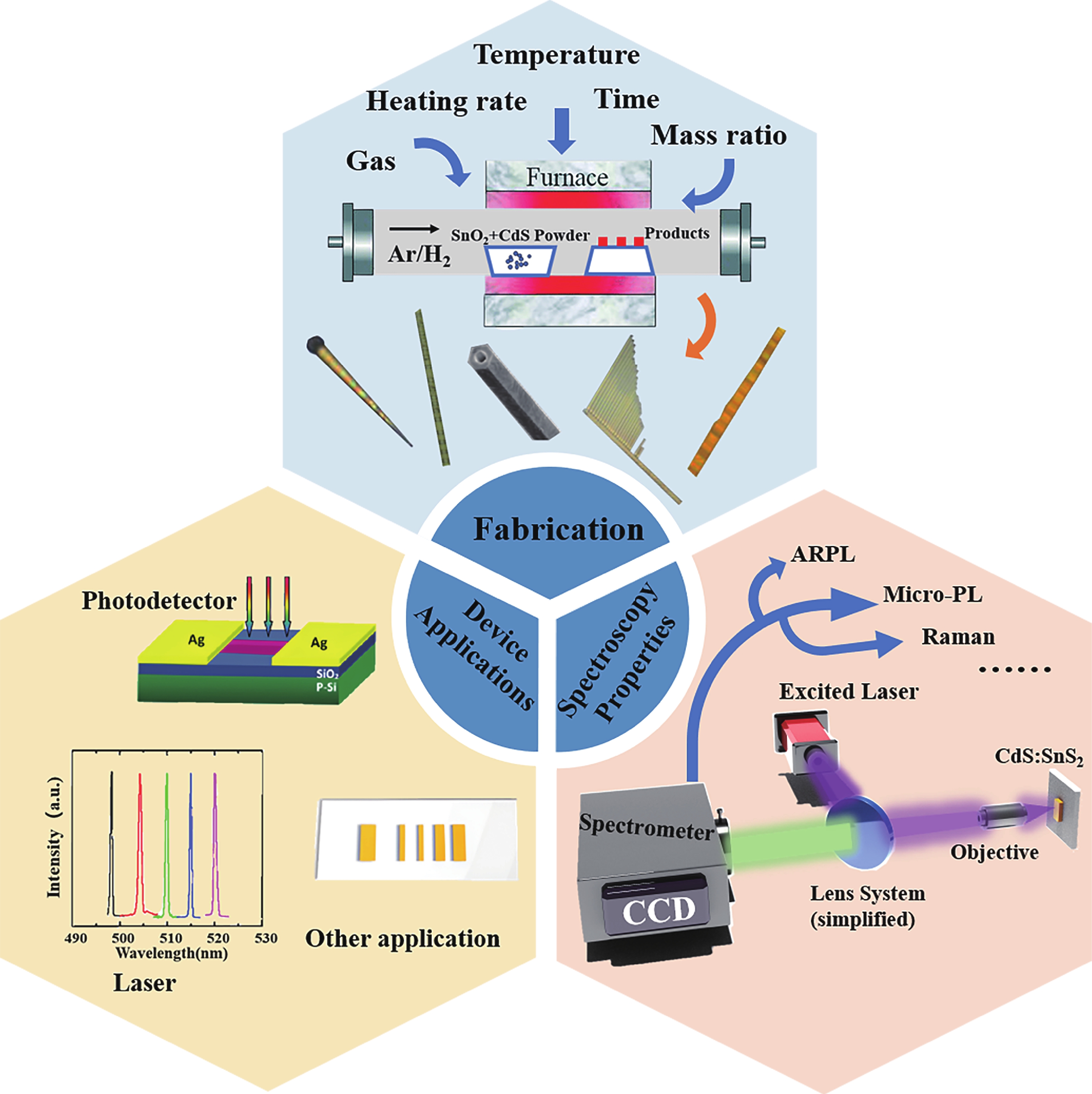
Fig. 1.  (Color online) Schematic illustration of the topics of this review, including the fabrication conditions, spectroscopy, and applications in Sn-doped CdS micro-nano structures.

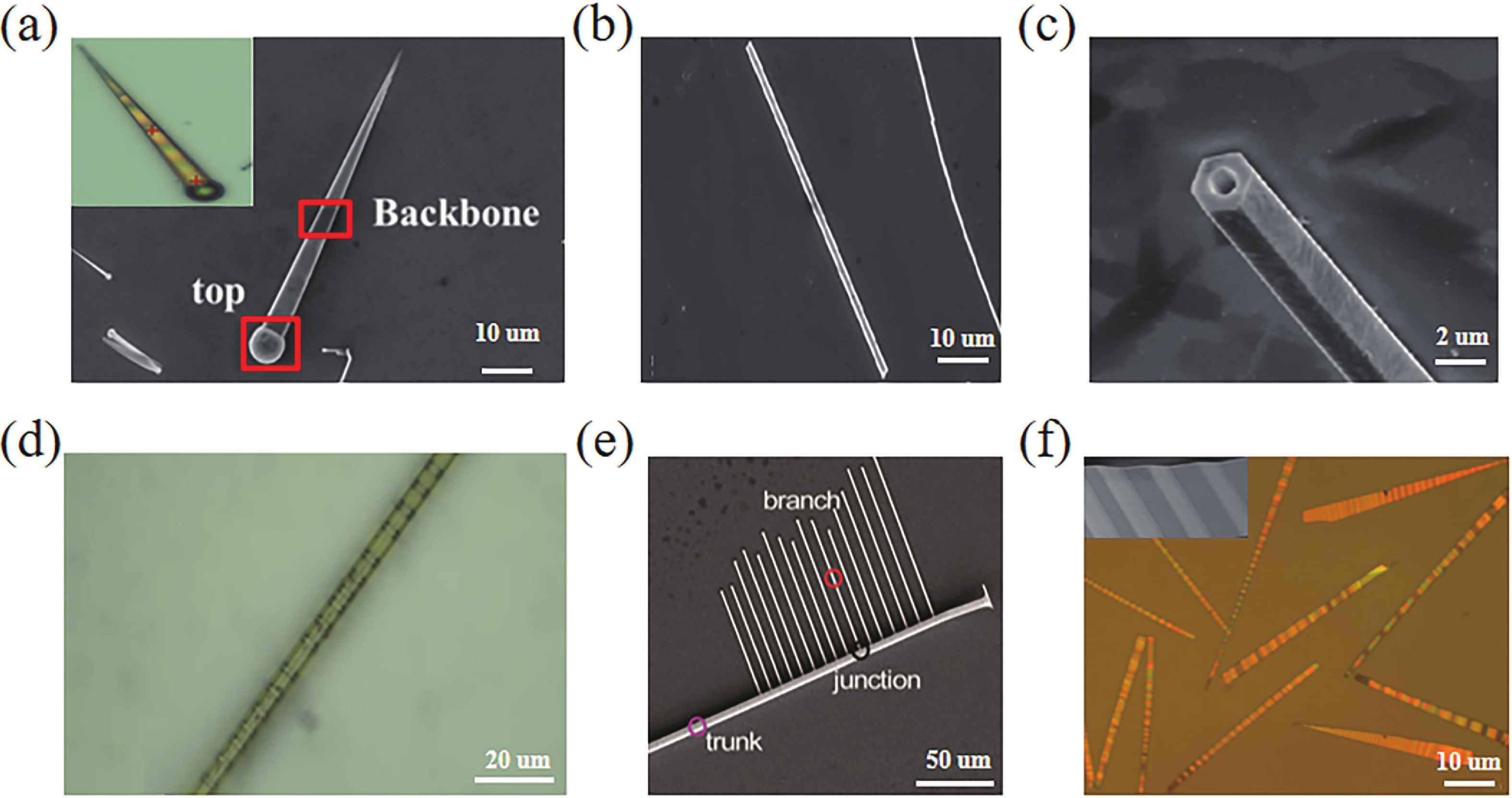
Fig. 2.  (Color online) Images of Sn-doped CdS samples with different nanostructures. (a) SEM image of microcones, with an inset showing the optical image of the superlattice structure[31]. (b) SEM image of nanowires. (c) SEM image of the core-shell structure[32]. (d) Optical image of superlattice nanowires. (e) SEM image of the comb-like nanostructure[33]. (f) Optical image of the nanobelt structure, with an inset showing the SEM image[34].

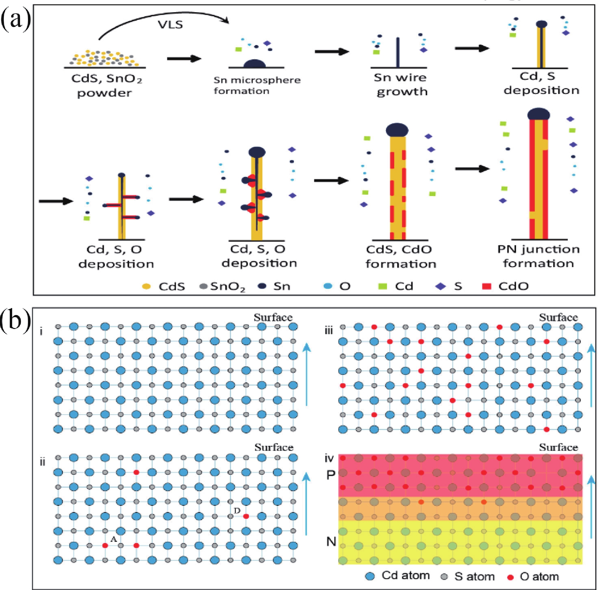
Fig. 3.  (Color online) (a) Schematic diagram of the growth process of core-shell structured nanowires. (b) Spatial distribution and local composition of O at different stages during the growth of CdS[39].

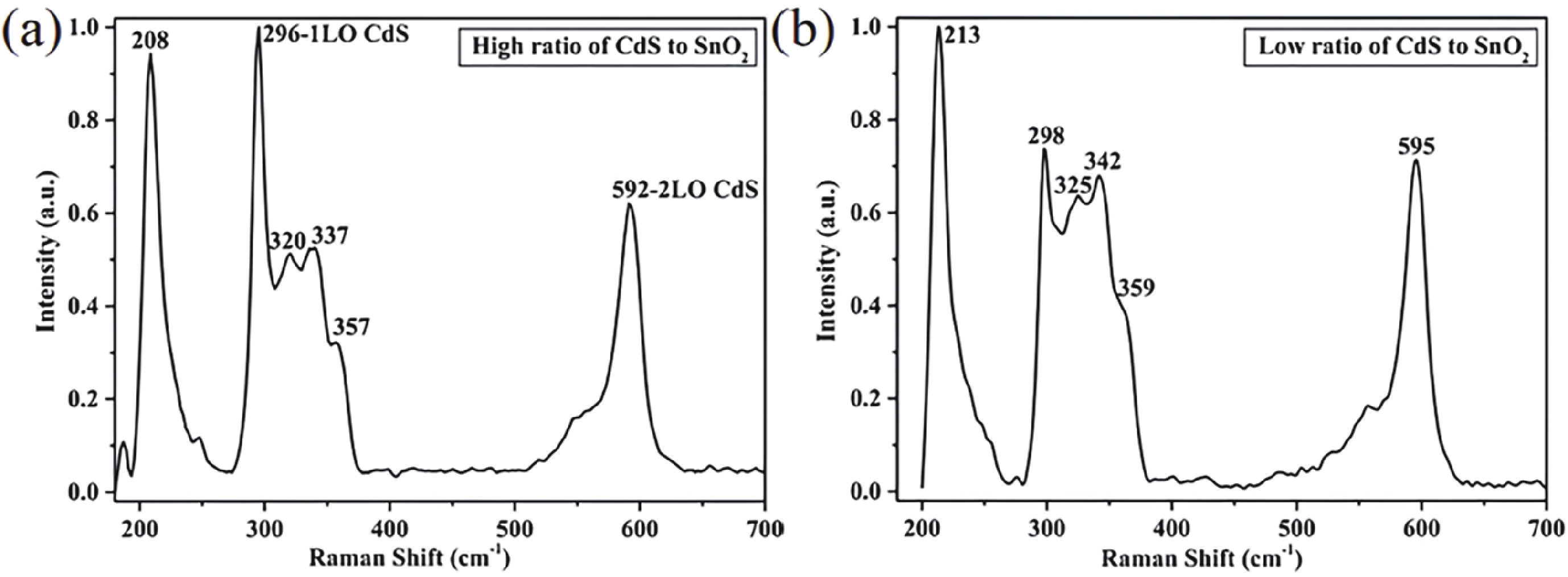
Fig. 4.  (a) and (b) are the micro Raman scattering spectra of single Sn-doped CdS nanowire with high and low CdS/SnO2 ratios, respectively[45].

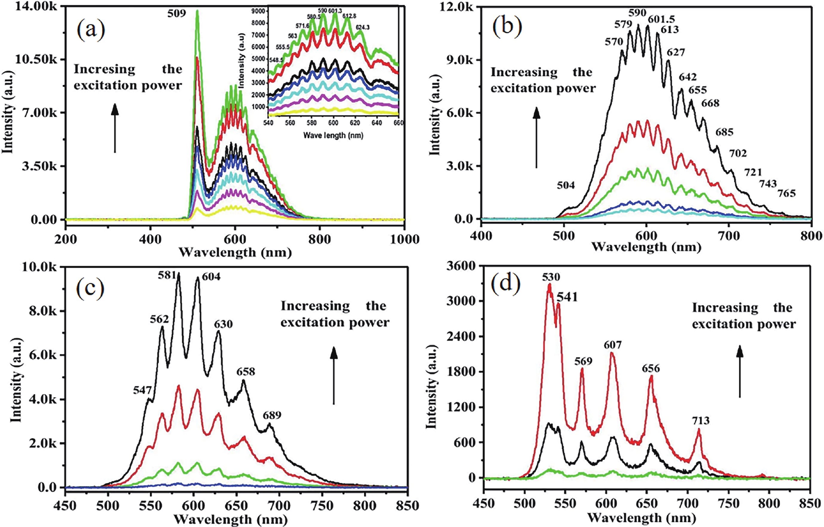
Fig. 5.  (Color online) (a)−(d) PL spectra of CdS nanowires with increasing Sn doping concentration[45].

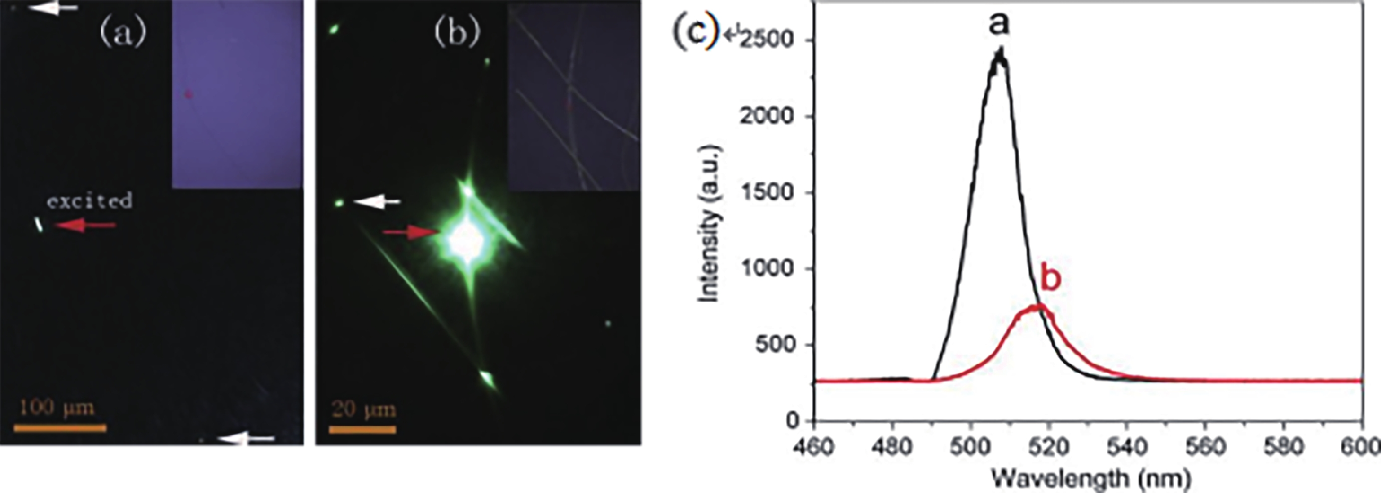
Fig. 6.  (Color online) Optical waveguide (a) and interconnect structure (b) of a single CdS nanowire 580 μm in length, illustrated with corresponding bright-field optical images, and (c) local far-field PL spectra of CdS nanowire with uncurved structure detected at excitation points a and emission points b[35].

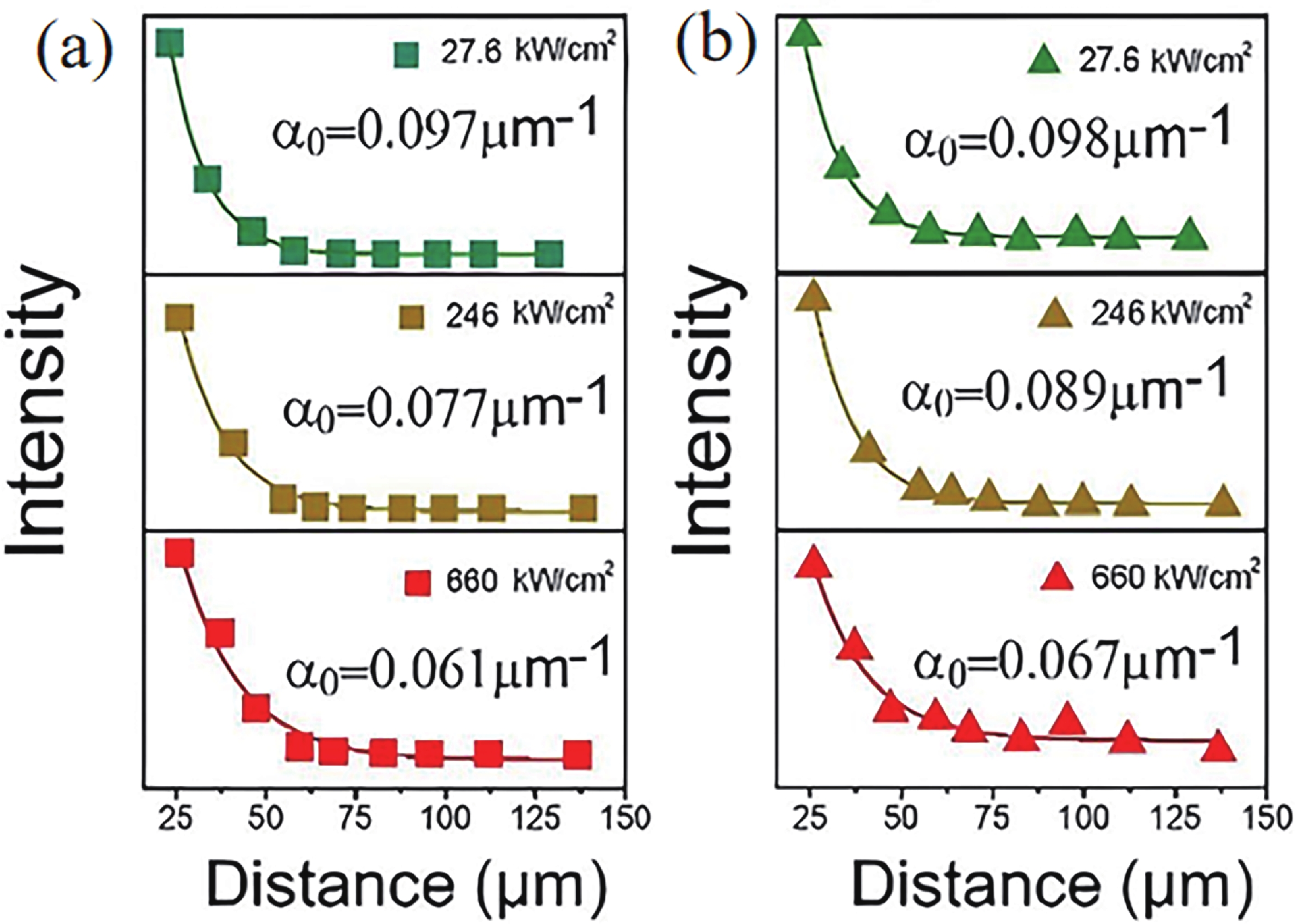
Fig. 7.  (Color online) (a) The relationship between near-band emission intensity and transmission distance at different excitation power densities. (b) The relationship between emission intensity and propagation distance of deep-level defects under different excitation power densities[49].

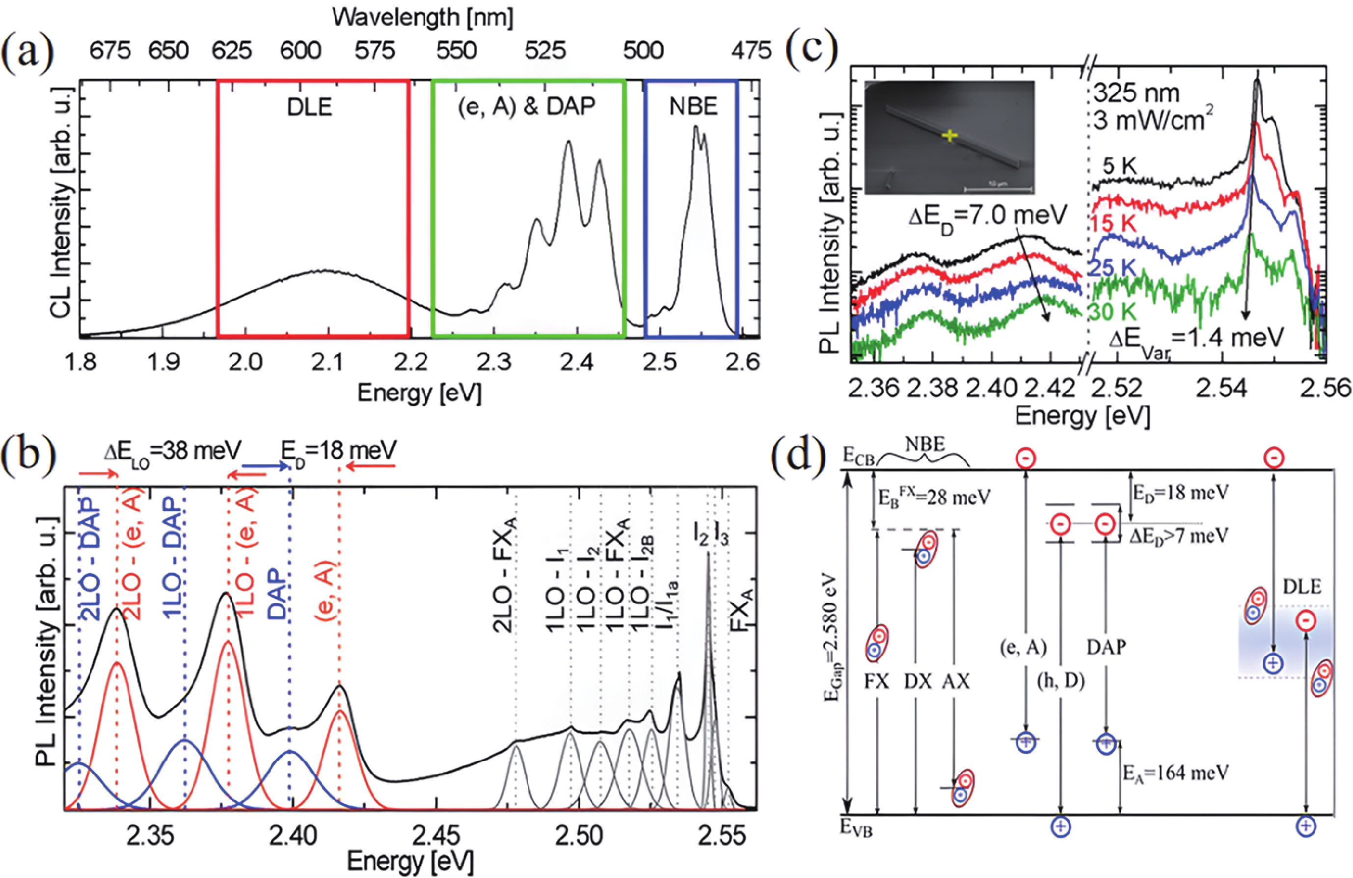
Fig. 8.  (Color online) (a) Low temperature (7 K) chemical spectra show three luminescence regions. (b) Photoluminescence spectra of Sn-doped CdS nanowire at 4 K. (c) Temperature-dependent μ-PL spectra of Sn-doped CdS nanowires. (d) Band structure of Sn-doped CdS nanowires and some exciton-non-exciton transitions[9].

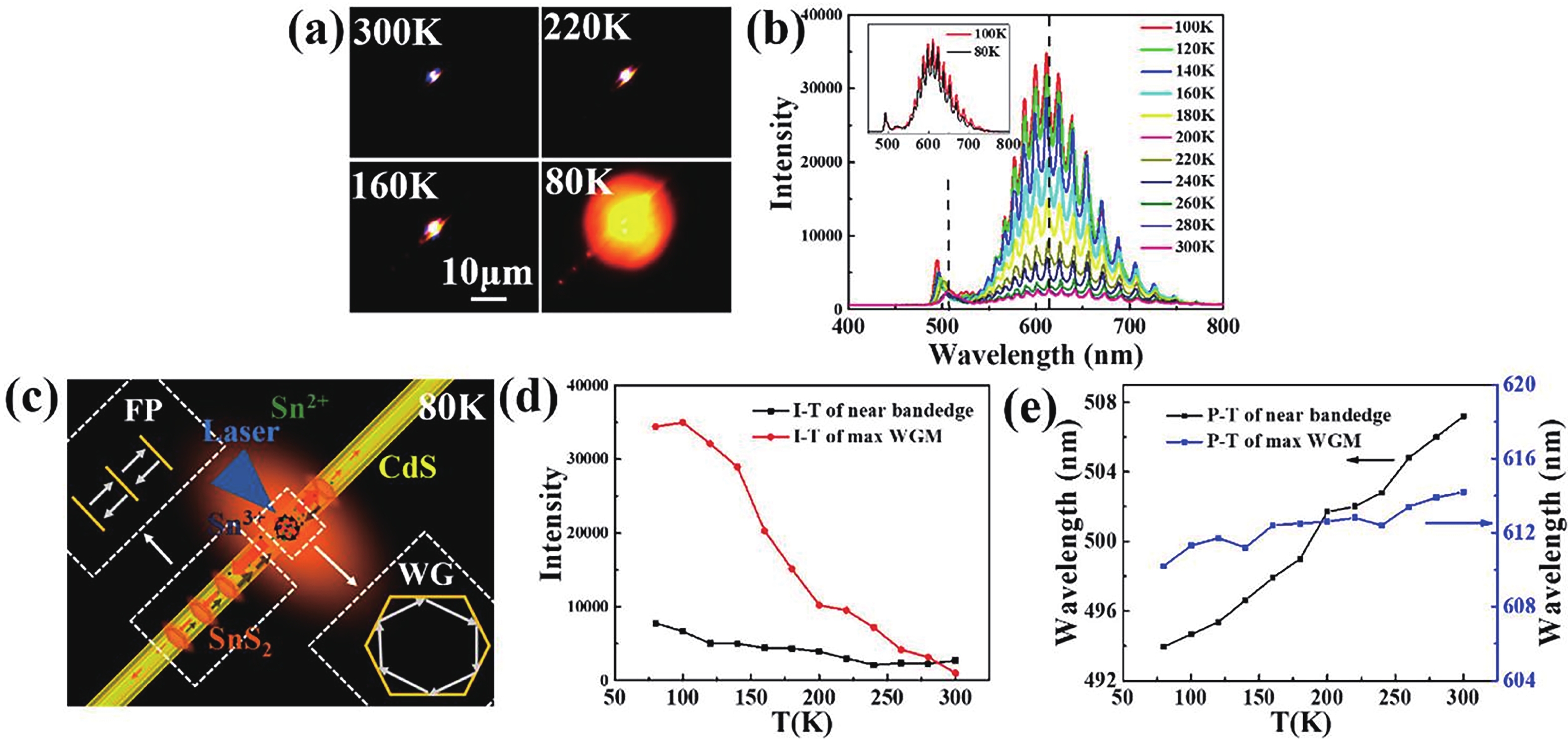
Fig. 9.  (Color online) (a) Images of Sn-doped CdS nanowires under dark-field microscopy at different temperatures. (b) Temperature-dependent PL spectra of a single Sn-doped CdS nanowire ranging from 100 to 300 K. The two black vertical dashed lines indicate the positions of the near-band-edge emission peak and the maximum WGM at 300 K. (c) Schematic diagram of the luminescence mechanism of Sn-doped nanowires at 80 K. (d) Temperature (T) dependence of the intensity I of the near-band-edge emission (black curve) and the maximum WGM (red curve). (e) Temperature (T) dependence of the peak positions P of the near-band-edge emission and the maximum WGM[52].

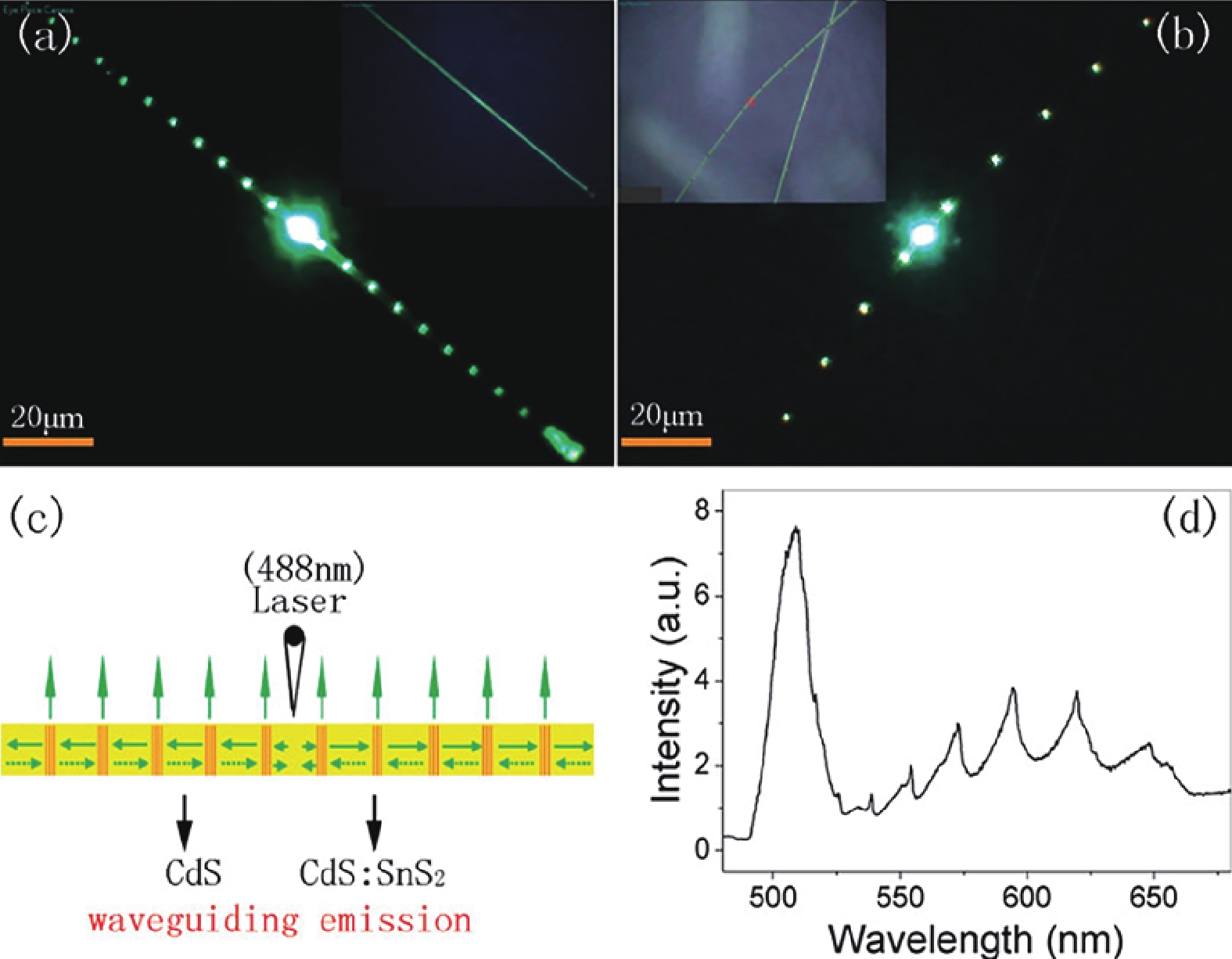
Fig. 10.  (Color online) Far-field PL images of excited samples at different reaction times: (a) 20 min; (b) 30 min. Insets in (a) and (b) are the corresponding optical images. (c) Schematic diagram of the emission process in 1D superlattice nanowires with λexc = 488 nm. (d) PL spectra of periodic CdS/CdS : SnS2 superlattice nanowires[37].

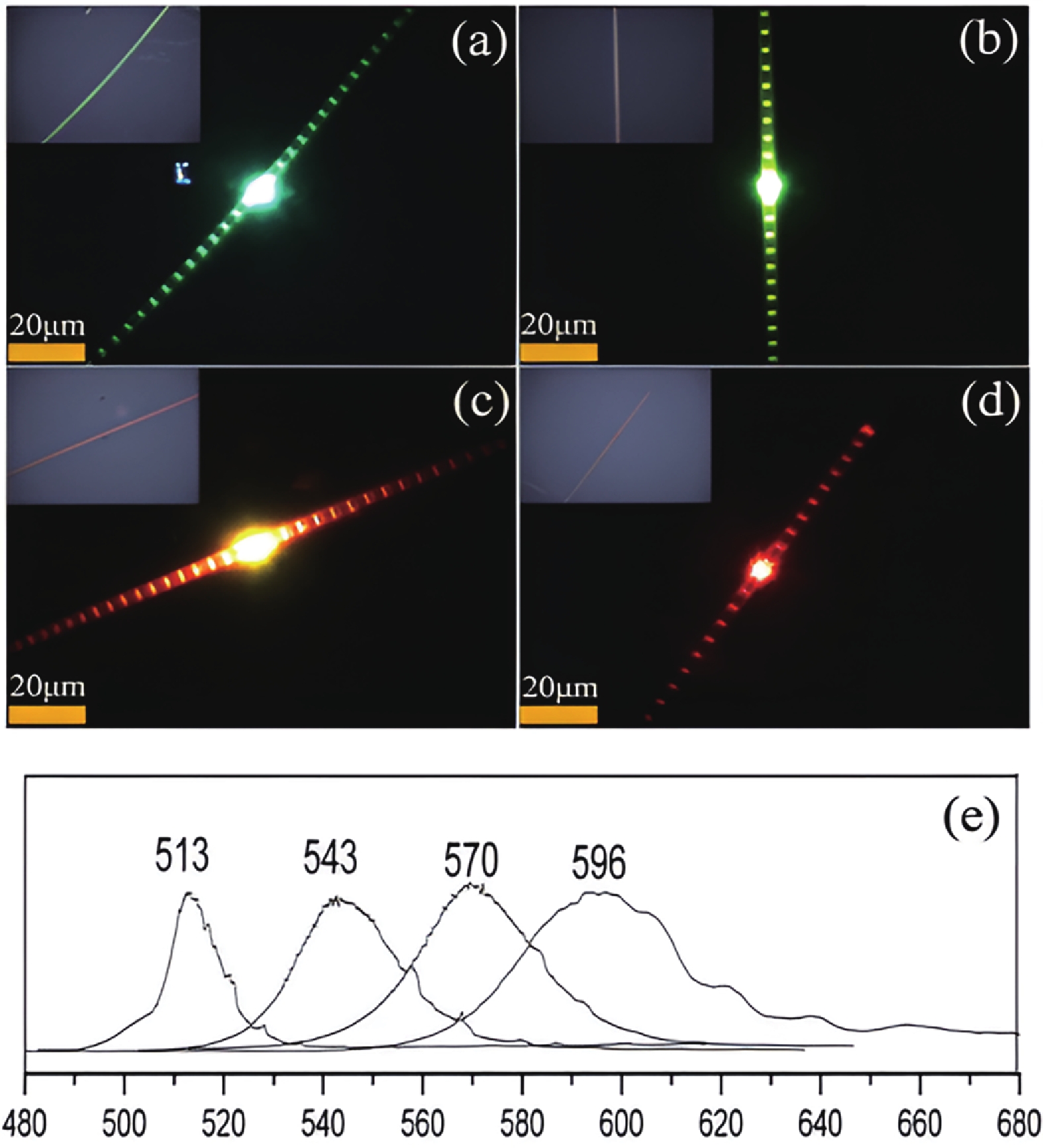
Fig. 11.  (Color online) (a)−(d) Dark-field PL images of CdS1−xSex/Sn : CdS1−xSex superlattice nanowires with x = 0, 0.1, 0.2, 0.4. Insets show the corresponding bright-field optical images. (e) Normalized PL spectra measured from (a)−(d)[38].

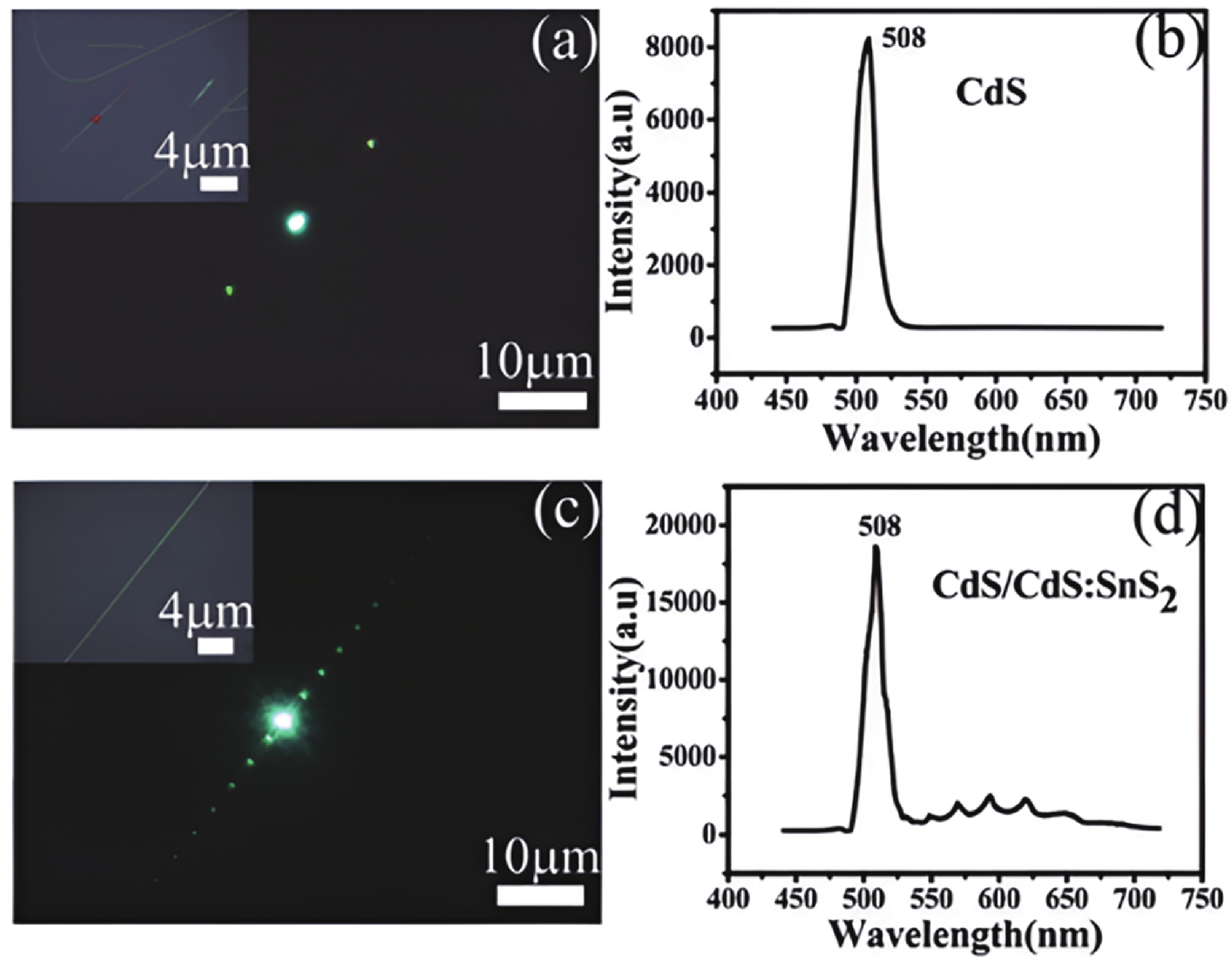
Fig. 12.  (Color online) (a) CdS nanowires and (c) CdS/CdS : SnS2 superlattice nanowires, with insets showing the corresponding optical images. (b) and (d) show the PL spectra of CdS nanowires and CdS/CdS : SnS2 superlattice nanowires, respectively[55].

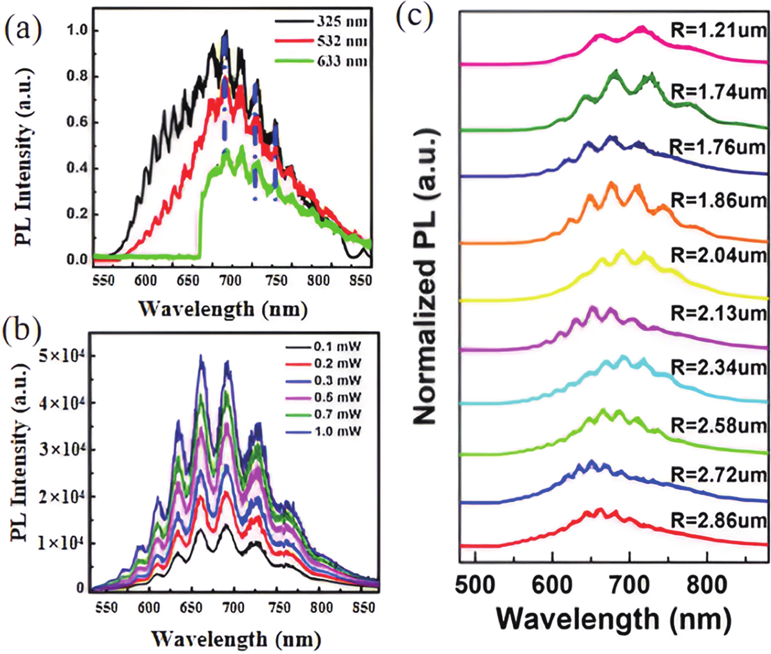
Fig. 13.  (Color online) (a) PL spectra of a single Sn-doped CdS micrometer under different excitation wavelengths of laser. (b) PL spectra of Sn-doped CdS microcone with increasing excitation power. (c) PL spectra of a single Sn-doped CdS microcone with different cross-sectional radii[31].

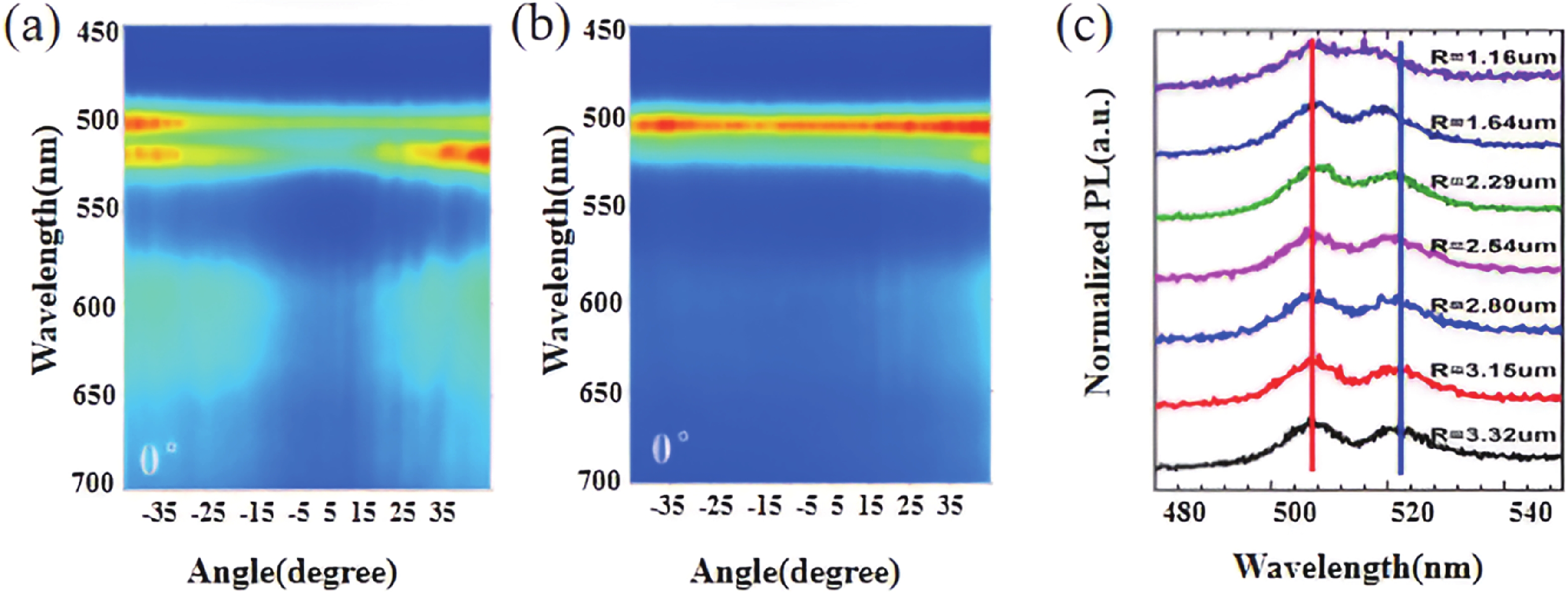
Fig. 14.  (Color online) (a) ARPL spectrum of the micrometer cone sample when perpendicular to the incident slit of the monochromator. (b) ARPL spectrum of the micrometer cone sample when parallel to the incident slit of the monochromator. (c) PL spectra of the micrometer cone with different cross-sectional radii[56].

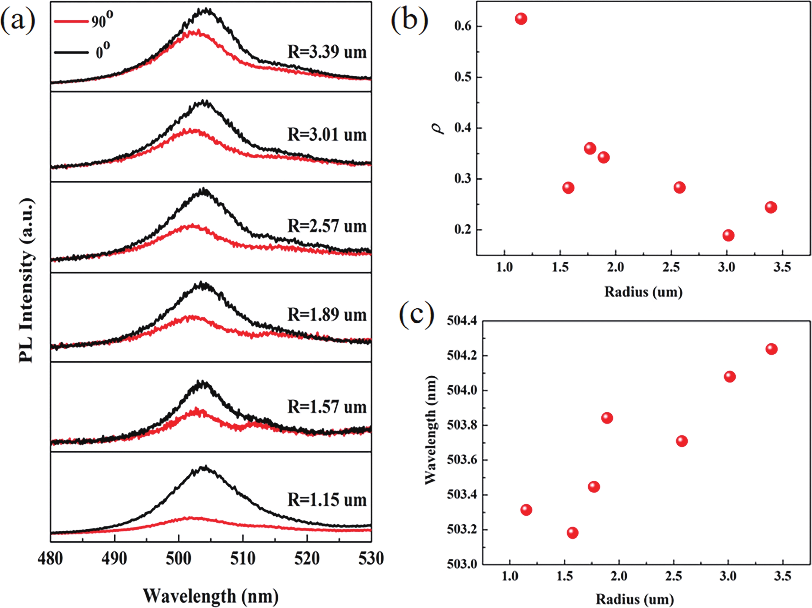
Fig. 15.  (Color online) (a) Radius-dependent circularly polarized PL spectra of Sn-doped CdS micrometer cones. (b) The relationship between the degree of polarization and the cross-sectional radius. (c) The relationship between the energy change in the PL spectra and the cross-sectional radius of Sn-doped CdS micrometer cones[57].

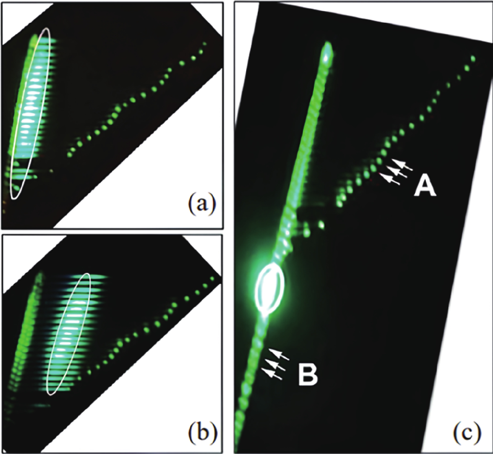
Fig. 16.  (Color online) (a) Lateral irradiation of the laser at the junction of the trunk and branch. (b) Irradiation of the laser at the central part of the branch. (c) Vertical irradiation of the laser at the position indicated by the white ellipse[40].

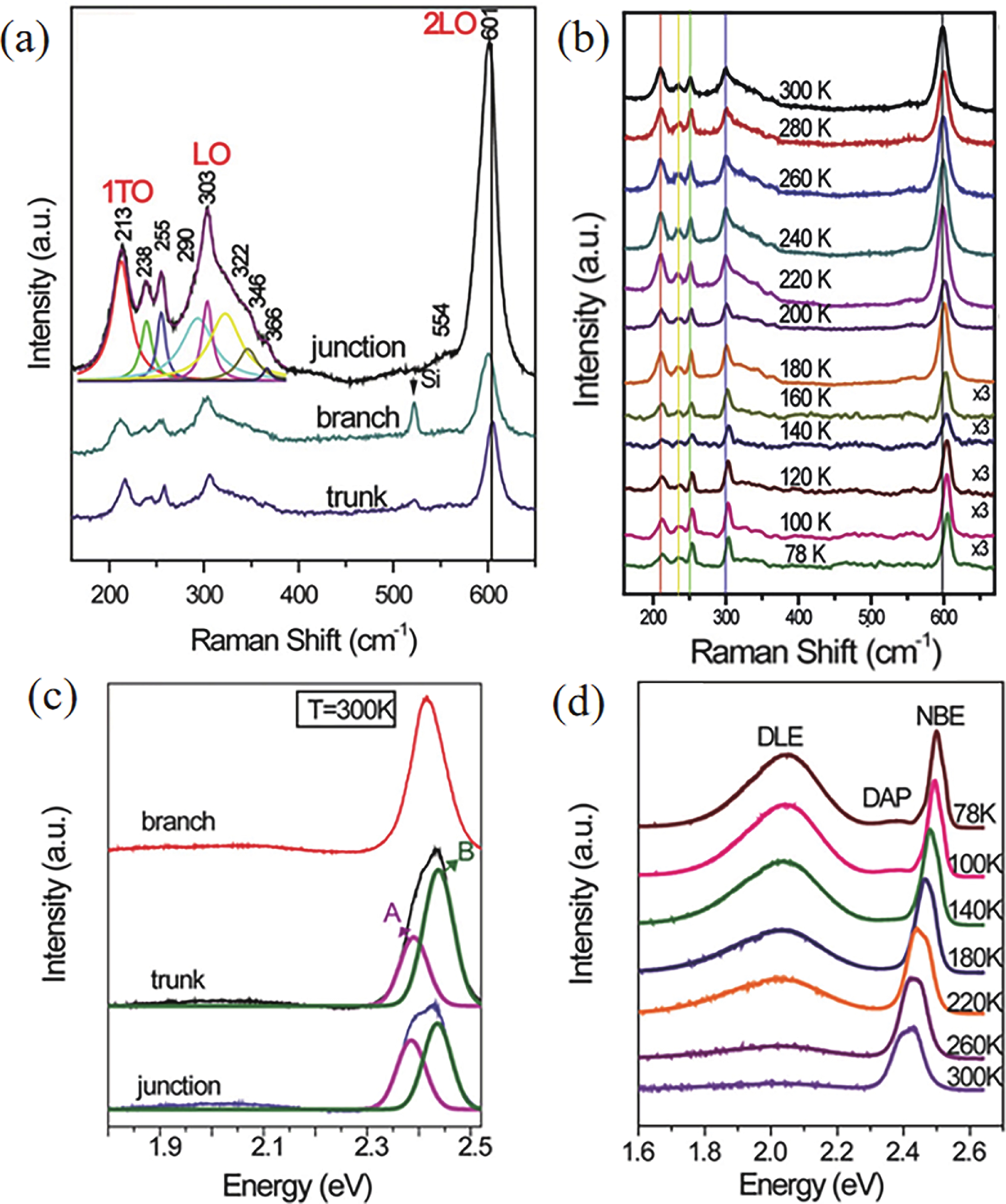
Fig. 17.  (Color online) (a) Room-temperature Raman spectra of different parts (junction/trunk/branch) of the CdS comb-like structure. (b) Raman spectra over a temperature range of 78−300 K. (c) Room-temperature photoluminescence spectra of different parts. (d) PL spectra at different temperatures[33].

Fig. 18.  (Color online) (a)−(c) Show the actual photoluminescence images at 2, 6, and 35 mW, respectively. (d) Variation of the intensity of green and red emissions with laser power. (e) Photoluminescence image of pure CdS comb-like nanostructures[61].

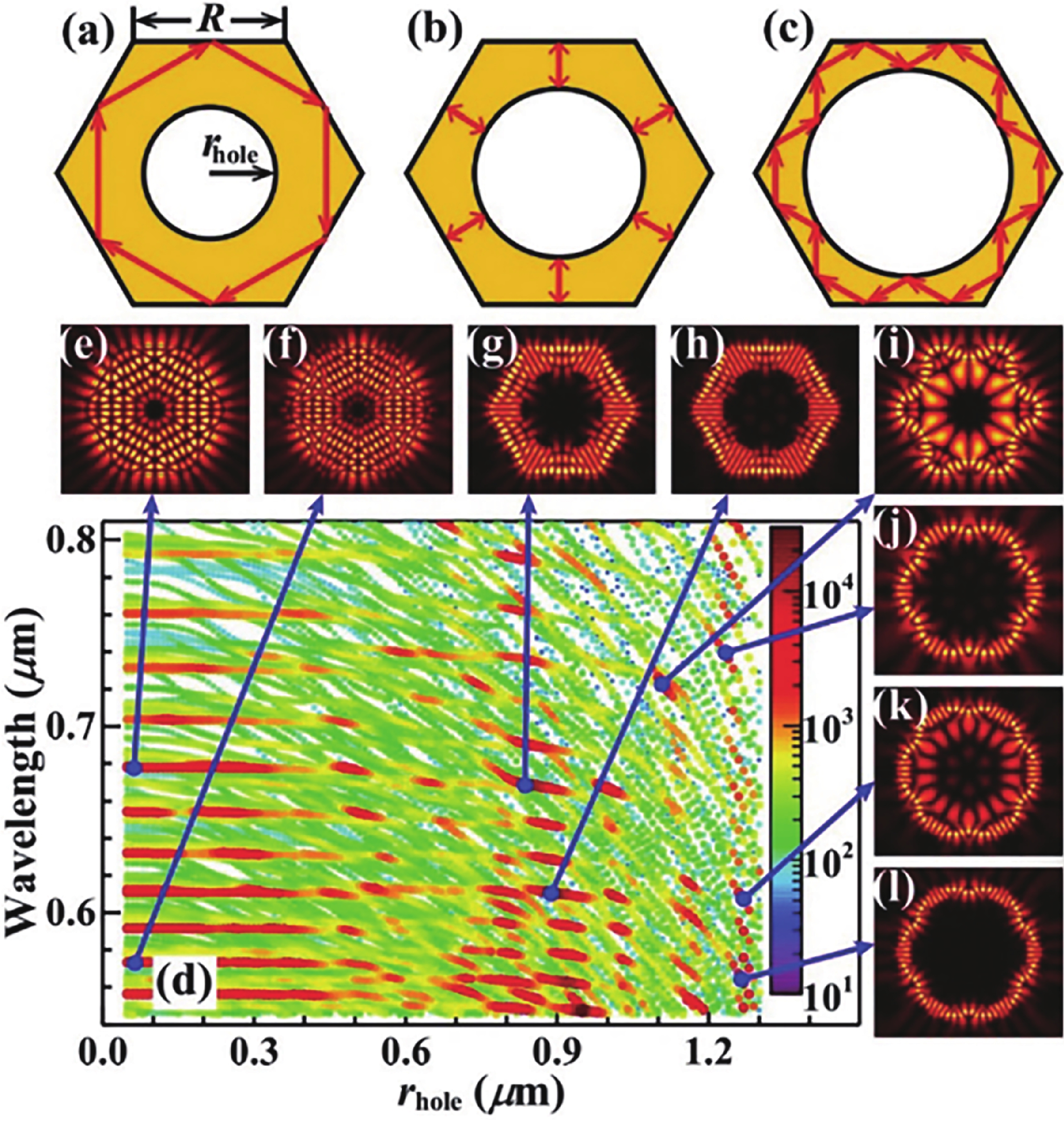
Fig. 19.  (Color online) Simulation analysis of luminescence modes in Sn-doped CdS porous structures with different wall thicknesses. (a)−(c) Schematic illustrations of radial optical propagation in hexagonal Sn-doped CdS porous structures with three different wall thicknesses, where the red arrows indicate the three existing mode propagation mechanisms. (d) Variation of Q with rhole and optical wavelength. (e)−(l) Electric field distributions of the eight high-Q modes corresponding to (d)[32].

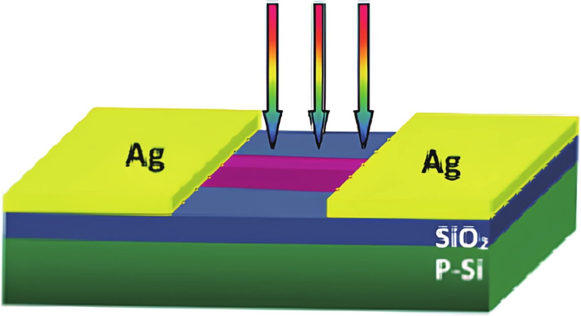
Fig. 20.  (Color online) Schematic diagram of a photodetector based on CdS/CdS : SnS2 superlattice nanowires[55].

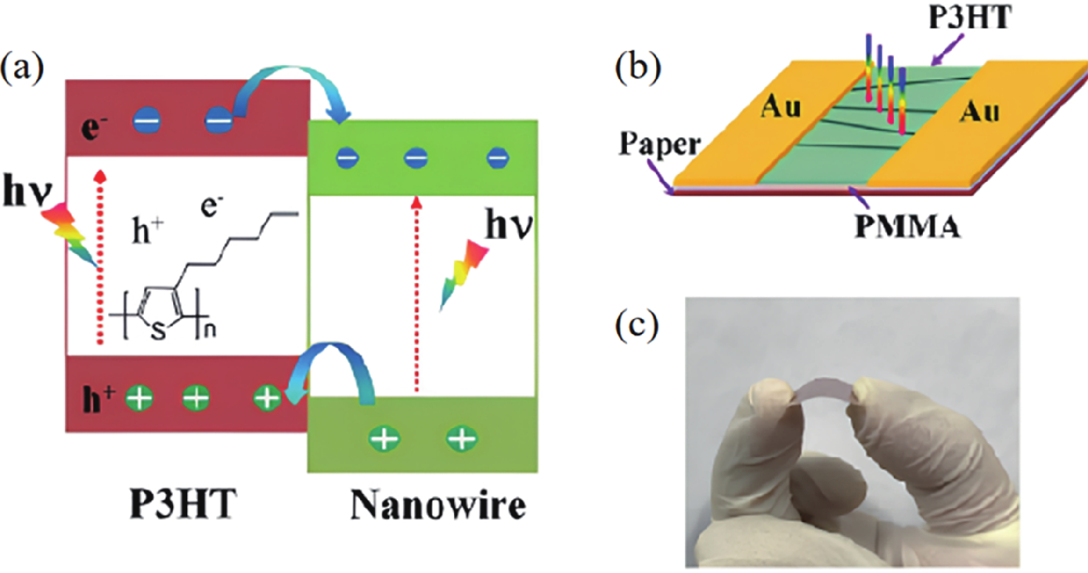
Fig. 21.  (Color online) (a) Schematic diagram of the energy band structure and carrier transfer in the hybrid P3HT-CdS/CdS : SnS2 superlattice nanowire structure. (b) Schematic diagram of the flexible hybrid film photodetector on paper substrate. (c) Actual image of the hybrid photodetector on paper substrate[68].

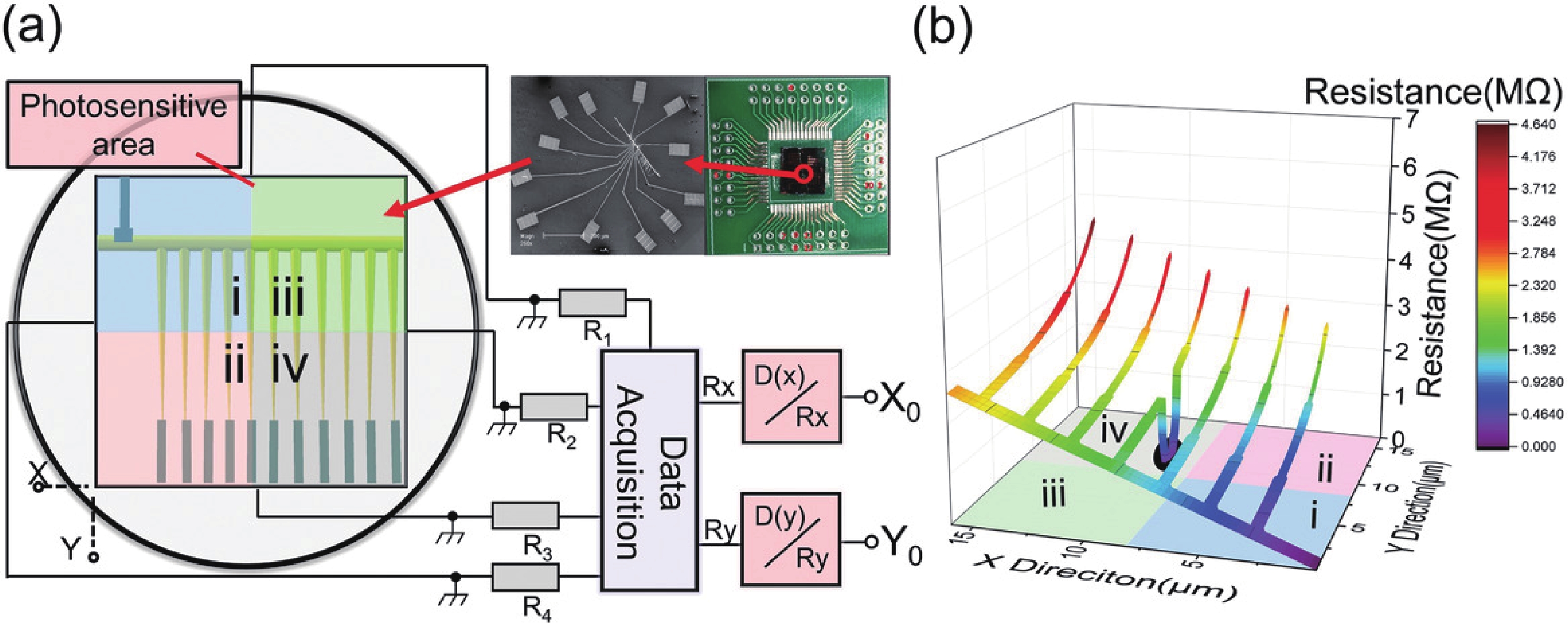
Fig. 22.  (Color online) (a) Schematic diagram of a four-quadrant photodetector. (b) Schematic diagram of the working principle of the designed photodetector[71].

Fig. 23.  (Color online) Schematic diagram of photodetector designed by Liu based on Sn-doped CdS nanowires[49].

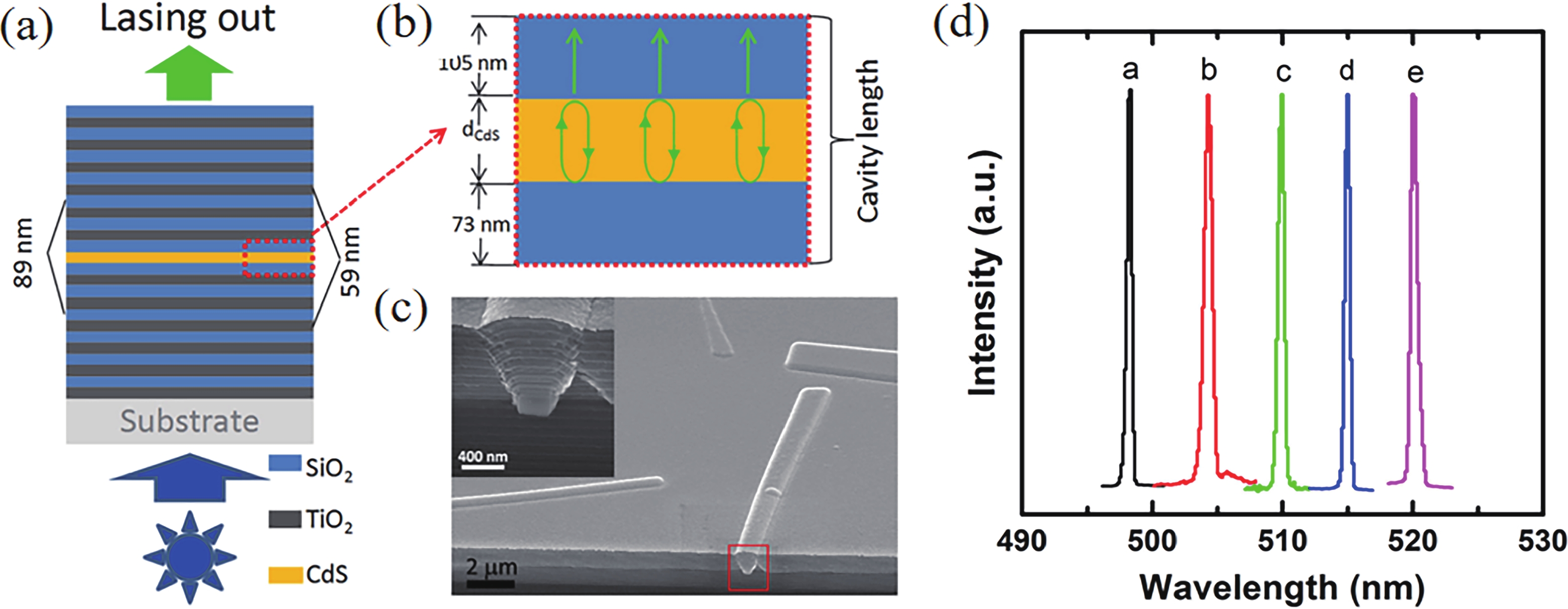
Fig. 24.  (Color online) (a) Schematic diagram of the design of a low-threshold single-mode laser. (b) Schematic illustration of the optical path between the CdS nanoribbons and the DBR. (c) SEM image of the physical device based on this design. (d) Laser spectra of CdS nanoribbons with different thicknesses embedded in the DBR microcavity[73].

Fig. 25.  (Color online) (a) Actual photograph of nanoribbons under laser excitation, with a scale bar of 20 μm. (b) PL spectra detected at different positions marked in (a)[34].

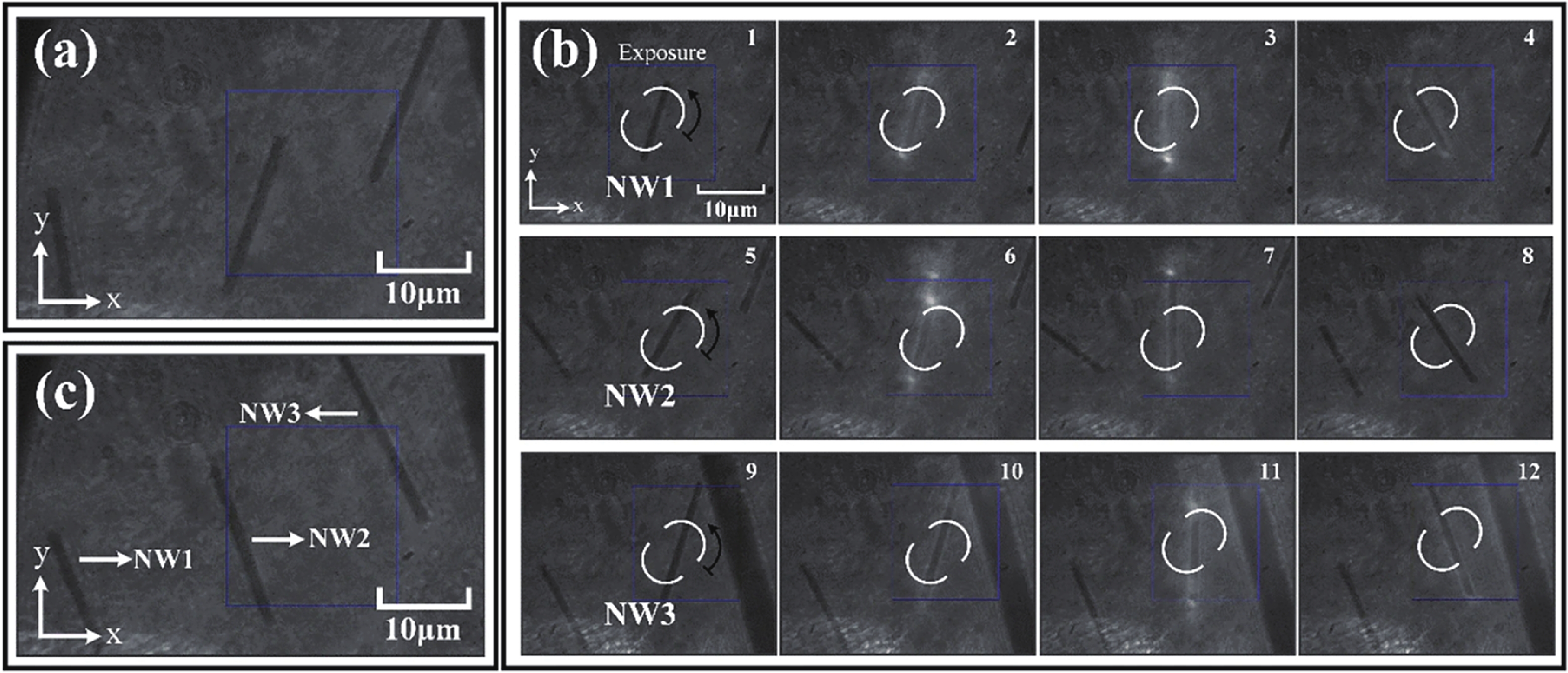
Fig. 26.  (Color online) Automatic alignment of disordered nanowires into an array. (a) Disordered CdS nanowires. (b) Alignment process of CdS nanowires. (c) Aligned array of nanowires[74].

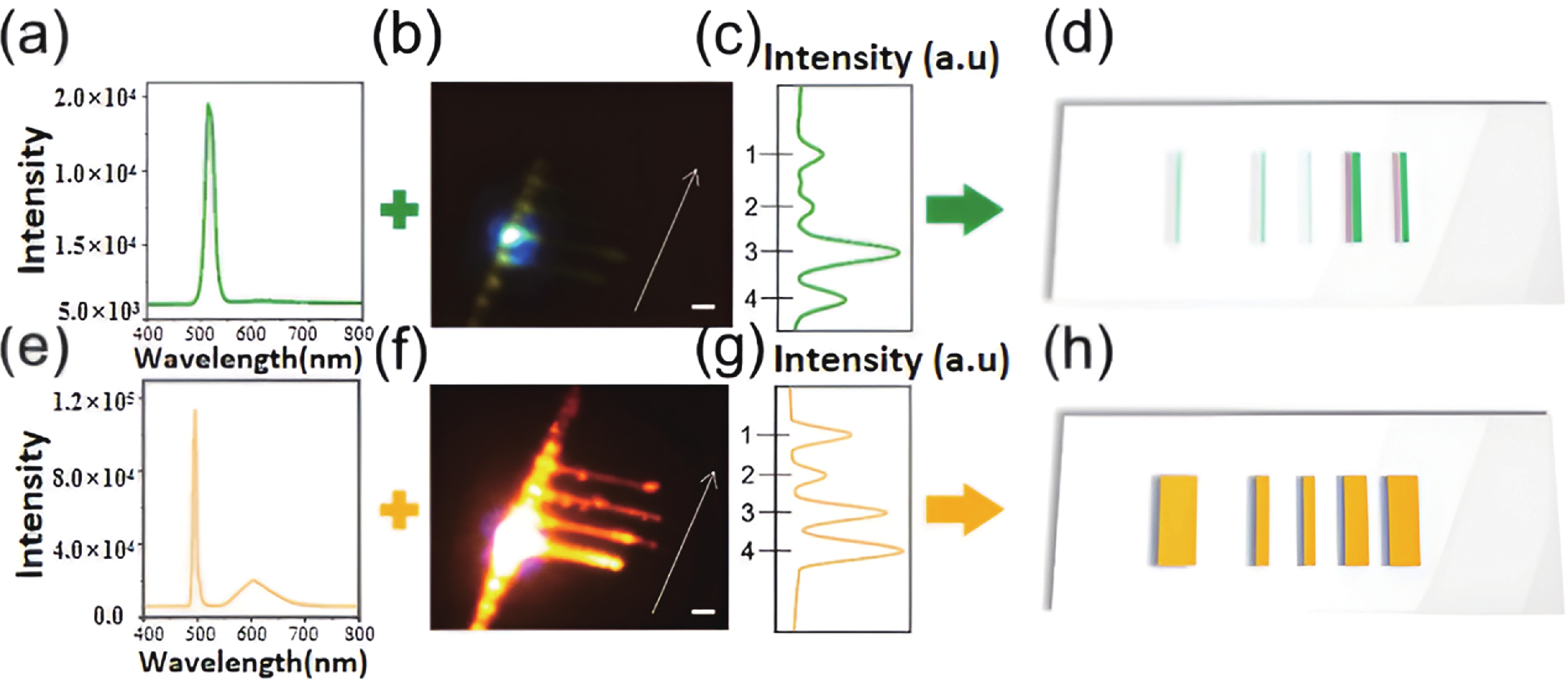
Fig. 27.  (Color online) (a) Spectrum at 300 K. (b) Physical images at 300 K. (c) Contours of corresponding intensity distributions at the ends of four different branches. (d) Barcode diagram at 300 K. (e)−(h) Images corresponding to room temperature conditions at 78 K[75].

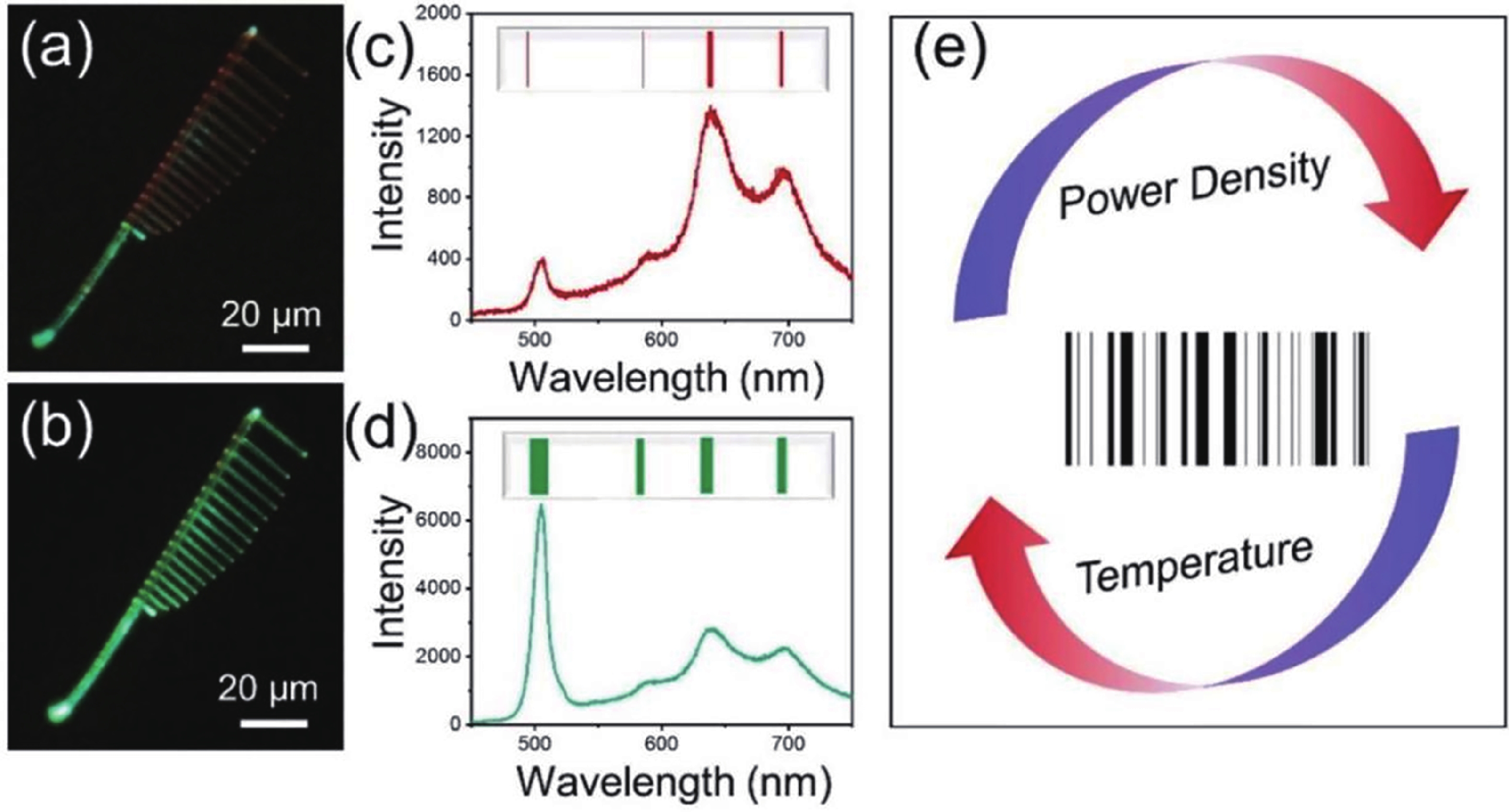
Fig. 28.  (Color online) (a) and (b) True color photoluminescence images of Sn-doped CdS comb nanostructures at different excitation powers. (c) and (d) Corresponding photogenic spectrum. (e) Coding strategy based on SN-doped CdS comb nanostructures[75].

Table 1.   Growth conditions for different Sn-doped CdS nanostructures.

Sample CdS : SnO2 Gas environment Heating rate
(°C/min)
Growth temperature
(°C)
Reaction time
(min)
Superlattice nanowire[37] 10 : 1 H2/Ar 10% 120 980 20−40
CdS/CdO core/shell nanowire[39] 1 : 1 Ar 40 1000 60
Comb-like nanostructure[40] 16 : 1−10 : 1 H2/Ar 10%−12% 70−100 1000 40−60
Nanowire[35] 10 : 1−0 H2/Ar 5% 100 1000 30
Core/shell nanowire[32] 20 : 1−10 : 1 H2/Ar 10% 90 900 15
Nanotube[32] 20 : 1−10 : 1 H2/Ar 10% 90 900 30
DownLoad: CSV
[1]
Cavin R K, Lugli P, Zhirnov V V. Science and engineering beyond Moore’s law. Proc IEEE, 2012, 100, 1720 doi: 10.1109/JPROC.2012.2190155
[2]
Haensch W, Nowak E J, Dennard R H, et al. Silicon CMOS devices beyond scaling. IBM J Res Dev, 2006, 50, 339 doi: 10.1147/rd.504.0339
[3]
Ye Y, Dai Y, Dai L, et al. High-performance single CdS nanowire (nanobelt) Schottky junction solar cells with Au/graphene Schottky electrodes. ACS Appl Mater Interfaces, 2010, 2, 3406 doi: 10.1021/am1007672
[4]
Jia C C, Lin Z Y, Huang Y, et al. Nanowire electronics: From nanoscale to macroscale. Chem Rev, 2019, 119, 9074 doi: 10.1021/acs.chemrev.9b00164
[5]
Yan R X, Gargas D, Yang P D. Nanowire photonics. Nature Photon, 2009, 3, 569 doi: 10.1038/nphoton.2009.184
[6]
Quan L N, Kang J, Ning C Z, et al. Nanowires for photonics. Chem Rev, 2019, 119, 9153 doi: 10.1021/acs.chemrev.9b00240
[7]
Chen C H, Chang S J, Chang S P, et al. Novel fabrication of UV photodetector based on ZnO nanowire/p-GaN heterojunction. Chem Phys Lett, 2009, 476, 69 doi: 10.1016/j.cplett.2009.06.007
[8]
Yang Z Y, Albrow-Owen T, Cui H, et al. Single-nanowire spectrometers. Science, 2019, 365, 1017 doi: 10.1126/science.aax8814
[9]
Zhang M, Wille M, Röder R, et al. Amphoteric nature of Sn in CdS nanowires. Nano Lett, 2014, 14, 518 doi: 10.1021/nl4035169
[10]
Granados del Águila A, Jha B, Pietra F, et al. Observation of the full exciton and phonon fine structure in CdSe/CdS dot-in-rod heteronanocrystals. ACS Nano, 2014, 8, 5921 doi: 10.1021/nn501026t
[11]
Scott R, Prudnikau A V, Antanovich A, et al. A comparative study demonstrates strong size tunability of carrier–phonon coupling in CdSe-based 2D and 0D nanocrystals. Nanoscale, 2019, 11, 3958 doi: 10.1039/C8NR09458F
[12]
Achtstein A W, Schliwa A, Prudnikau A, et al. Electronic structure and exciton–phonon interaction in two-dimensional colloidal CdSe nanosheets. Nano Lett, 2012, 12, 3151 doi: 10.1021/nl301071n
[13]
Achermann M, Bartko A P, Hollingsworth J A, et al. The effect of Auger heating on intraband carrier relaxation in semiconductor quantum rods. Nat Phys, 2006, 2, 557 doi: 10.1038/nphys363
[14]
Klimov V I. Optical nonlinearities and ultrafast carrier dynamics in semiconductor nanocrystals. J Phys Chem B, 2000, 104, 6112 doi: 10.1021/jp9944132
[15]
Hou X Q, Kang J, Qin H Y, et al. Engineering Auger recombination in colloidal quantum dots via dielectric screening. Nat Commun, 2019, 10, 1750 doi: 10.1038/s41467-019-09737-2
[16]
Wang Y, Sun H D. Advances and prospects of lasers developed from colloidal semiconductor nanostructures. Prog Quant Electron, 2018, 60, 1 doi: 10.1016/j.pquantelec.2018.05.002
[17]
Jang J, Song G, Kyhm K, et al. Optical gain of inelastic exciton-exciton scattering in CdS nanowires. Appl Phys Lett, 2019, 114, 1101 doi: 10.1063/1.5086782
[18]
Zhang Z, Wang Y L, Yin S Y, et al. Exciton-polariton light-emitting diode based on a ZnO microwire. Opt Express, 2017, 25, 17375 doi: 10.1364/OE.25.017375
[19]
Chen J Y, Wong T M, Chang C W, et al. Self-polarized spin-nanolasers. Nature Nanotech, 2014, 9, 845 doi: 10.1038/nnano.2014.195
[20]
Zhao Z, Zhong M Y, Zhou W C, et al. Simultaneous triplet exciton–phonon and exciton–photon photoluminescence in the individual weak confinement CsPbBr3 micro/nanowires. J Phys Chem C, 2019, 123, 25349 doi: 10.1021/acs.jpcc.9b06643
[21]
Takagahara T. Electron−phonon interactions in semiconductor nanocrystals. J Lumin, 1996, 70, 129 doi: 10.1016/0022-2313(96)00050-6
[22]
Zheng Q, Zhou W C, Peng Y H, et al. Surface polarons and optical micro-cavity modulated broad range multi-mode emission of Te-doped CdS nanowires. Nanotechnology, 2018, 29, 465709 doi: 10.1088/1361-6528/aadf64
[23]
Lai Y Y, Lan Y P, Lu T C. Strong light–matter interaction in ZnO microcavities. Light Sci Appl, 2013, 2, e76 doi: 10.1038/lsa.2013.32
[24]
Tawara T, Yoshida H, Yogo T, et al. Microcavities with distributed Bragg reflectors based on ZnSe/MgS superlattice grown by MOVPE. J Cryst Growth, 2000, 221, 699 doi: 10.1016/S0022-0248(00)00803-4
[25]
Claudon J, Bleuse J, Malik N S, et al. A highly efficient single-photon source based on a quantum dot in a photonic nanowire. Nat Photonics, 2010, 4, 174 doi: 10.1038/nphoton.2009.287x
[26]
Mak K F, Shan J. Photonics and optoelectronics of 2D semiconductor transition metal dichalcogenides. Nature Photon, 2016, 10, 216 doi: 10.1038/nphoton.2015.282
[27]
Fang K J, Matheny M H, Luan X S, et al. Optical transduction and routing of microwave phonons in cavity-optomechanical circuits. Nat Photonics, 2016, 10, 489 doi: 10.1038/nphoton.2016.107
[28]
Tochitsky I, Trautman J, Gallerani N, et al. Restoring visual function to the blind retina with a potent, safe and long-lasting photoswitch. Sci Rep, 2017, 7, 45487 doi: 10.1038/srep45487
[29]
van Vugt L K, Rühle S, Ravindran P, et al. Exciton polaritons confined in a ZnO nanowire cavity. Phys Rev Lett, 2006, 97, 147401 doi: 10.1103/PhysRevLett.97.147401
[30]
Stevenson R M, Salter C L, Nilsson J, et al. Indistinguishable entangled photons generated by a light-emitting diode. Phys Rev Lett, 2012, 108, 040503 doi: 10.1103/PhysRevLett.108.040503
[31]
Tian Y, Peng H, Yao S, et al. Repeatedly and superbroad savelength tuning microcavity in a single Sn-doped CdS microcone. J Phys Chem C, 2022, 126, 12696 doi: 10.1021/acs.jpcc.2c04142
[32]
Zhang L, Zhang Y, Guo Y, et al. Growth of CdS nanotubes and their strong optical microcavity effects. Nanoscale, 2019, 11, 5325 doi: 10.1039/C8NR10323B
[33]
Song G L, Guo S, Wang X X, et al. Temperature dependent Raman and photoluminescence of an individual Sn-doped CdS branched nanostructure. New J Phys, 2015, 17, 063024 doi: 10.1088/1367-2630/17/6/063024
[34]
Zhang Q L, Zhu X L, Li Y Y, et al. Nanolaser arrays based on individual waved CdS nanoribbons. Laser Photonics Rev, 2016, 10, 458 doi: 10.1002/lpor.201500268
[35]
Dai G Z, Wan Q, Zhou C J, et al. Sn-catalyst growth and optical waveguide of ultralong CdS nanowires. Chem Phys Lett, 2010, 497, 85 doi: 10.1016/j.cplett.2010.07.095
[36]
Dai B B, Fan C, Xu X, et al. Growing a CdS flag from a wire with in situ control of the catalyst. CrystEngComm, 2021, 23, 3664 doi: 10.1039/D1CE00289A
[37]
Dai G Z, Zou B S, Wang Z L. Preparation and periodic emission of superlattice CdS/CdS: SnS2 microwires. J Am Chem Soc, 2010, 132, 12174 doi: 10.1021/ja1037963
[38]
Dai G Z, Liu R B, Wan Q, et al. Color-tunable periodic spatial emission of alloyed CdS1-xSex/Sn: CdS1-xSex superlattice microwires. Opt Mater Express, 2011, 1, 1185 doi: 10.1364/OME.1.001185
[39]
Zou S Y, Zhou W C, Liu R B, et al. Cavity-enhanced microphotoluminescence in a core–shell n–p CdS/CdO micrometer wire and Its efficient surface photovoltage responses in the whole visible range. J Phys Chem C, 2017, 121, 14349 doi: 10.1021/acs.jpcc.7b04053
[40]
Liu R B, Li Z A, Zhang C H, et al. Single-step synthesis of monolithic comb-like CdS nanostructures with tunable waveguide properties. Nano Lett, 2013, 13, 2997 doi: 10.1021/nl401726z
[41]
Arguello C A, Rousseau D L, Porto S P S. First-order Raman effect in wurtzite-type crystals. Phys Rev, 1969, 181, 1351 doi: 10.1103/PhysRev.181.1351
[42]
Smith A J, Meek P E, Liang W Y. Raman scattering studies of SnS2 and SnSe2. J Phys C Solid State Phys, 1977, 10, 1321 doi: 10.1088/0022-3719/10/8/035
[43]
Zhou W C, Liu R B, Wan Q, et al. Bound exciton and optical properties of SnO2 one-dimensional nanostructures. J Phys Chem C, 2009, 113, 1719 doi: 10.1021/jp808422a
[44]
Abello L, Bochu B, Gaskov A, et al. Structural characterization of nanocrystalline SnO2 by X-ray and Raman spectroscopy. J Solid State Chem, 1998, 135, 78 doi: 10.1006/jssc.1997.7596
[45]
Peng Y H, Luo Y, Zhou W C, et al. Photoluminescence and boosting electron-phonon coupling in CdS nanowires with variable Sn(IV) dopant concentration. Nanoscale Res Lett, 2021, 16, 19 doi: 10.1186/s11671-021-03485-3
[46]
Scott J F, Damen T C, Silfvast W T, et al. Resonant Raman scattering in ZnS and ZnSe with the cadmium laser. Opt Commun, 1970, 1, 397 doi: 10.1016/0030-4018(70)90081-7
[47]
Pan A L, Liu R B, Zou B S. Phonon-assisted stimulated emission from single CdS nanoribbons at room temperature. Appl Phys Lett, 2006, 88, 3102 doi: 10.1063/1.2198089
[48]
Xu J Y, Zhuang X J, Guo P F, et al. Dilute tin-doped CdS nanowires for low-loss optical waveguiding. J Mater Chem C, 2013, 1, 4391 doi: 10.1039/c3tc30492b
[49]
Guo S, Wang L, Ding C J, et al. Tunable optical loss and multi-band photodetection based on tin doped CdS nanowire. J Alloys Compd, 2020, 835, 155330 doi: 10.1016/j.jallcom.2020.155330
[50]
Aguilar-Hern ndez J, Contreras-Puente G, Morales-Acevedo A, et al. Photoluminescence and structural properties of cadmium sulphide thin films grown by different techniques. Semicond Sci Technol, 2003, 18, 111 doi: 10.1088/0268-1242/18/2/308
[51]
Varshni Y P. Temperature dependence of the energy gap in semiconductors. Physica, 1967, 34, 149 doi: 10.1016/0031-8914(67)90062-6
[52]
Zhang L, Liu R B, Zou B S. Sn-doped CdS nanowires with low-temperature lasing by CW-laser excitation. ACS Appl Electron Mater, 2020, 2, 282 doi: 10.1021/acsaelm.9b00766
[53]
Liu B, Chen R, Xu X L, et al. Exciton-related photoluminescence and lasing in CdS nanobelts. J Phys Chem C, 2011, 115, 12826 doi: 10.1021/jp203551f
[54]
Notomi M, Kuramochi E, Tanabe T. Large-scale arrays of ultrahigh-Q coupled nanocavities. Nature Photon, 2008, 2, 741 doi: 10.1038/nphoton.2008.226
[55]
Gou G Y, Dai G Z, Qian C, et al. High-performance ultraviolet photodetectors based on CdS/CdS: SnS2 superlattice nanowires. Nanoscale, 2016, 8, 14580 doi: 10.1039/C6NR02915A
[56]
Tian Y, Zhang Y Y, Peng H, et al. Revealing the quantum-confined free exciton A anisotropic emission in a CdS/CdS: SnS2 superlattice nanocone via angle-resolved photoluminescence spectroscopy. J Phys Chem C, 2022, 126, 1064 doi: 10.1021/acs.jpcc.1c09755
[57]
Tian Y, Yao S F, Lin W C, et al. Effect of quantum confinement on polarization anisotropy emission in Sn-doped CdS microcones. Mater Adv, 2022, 3, 8407 doi: 10.1039/D2MA00883A
[58]
Maslov A V, Ning C Z. Radius-dependent polarization anisotropy in semiconductor nanowires. Phys Rev B, 2005, 72, 161310 doi: 10.1103/PhysRevB.72.161310
[59]
Guo S, Liu R B, Niu C H, et al. Tin nanoparticles–enhanced optical transportation in branched CdS nanowire waveguides. Adv Opt Mater, 2018, 6, 1800305 doi: 10.1002/adom.201800305
[60]
Zhou W C, Tang D S, Liu R B, et al. Structure and optical properties of pure and doped ZnO 1D nanostructures. Mate Lett, 2013, 91, 369 doi: 10.1016/j.matlet.2012.10.041
[61]
Guo S, Zhao F Y, Li Y, et al. Individual dual-emitting CdS multi-branched nanowire arrays under various pumping powers. Appl Phys Lett, 2016, 109, 162101 doi: 10.1063/1.4964879
[62]
Liu R B, Chen Y J, Wang F F, et al. Stimulated emission from trapped excitons in SnO2 nanowires. Physica E Low Dimension Syst Nanostruct, 2007, 39, 223 doi: 10.1016/j.physe.2007.04.009
[63]
Zhang Q L, Liu H W, Guo P F, et al. Vapor growth and interfacial carrier dynamics of high-quality CdS-CdSSe-CdS axial nanowire heterostructures. Nano Energy, 2017, 32, 28 doi: 10.1016/j.nanoen.2016.12.014
[64]
Li L, Yang S M, Han F, et al. Optical sensor based on a single CdS nanobelt. Sensors, 2014, 14, 7332 doi: 10.3390/s140407332
[65]
Zhou W C, Peng Y H, Yin Y L, et al. Broad spectral response photodetector based on individual tin-doped CdS nanowire. AIP Adv, 2014, 4, 3005 doi: 10.1063/1.4897521
[66]
Jie J S, Zhang W J, Jiang Y, et al. Photoconductive characteristics of single-crystal CdS nanoribbons. Nano Leet, 2006, 6, 1887 doi: 10.1021/nl060867g
[67]
Zhou W C, Zhou Y, Peng Y H, et al. Ultrahigh sensitivity and gain white light photodetector based on GaTe/Sn: CdS nanoflake/nanowire heterostructures. Nanotechnology, 2014, 25, 445202 doi: 10.1088/0957-4484/25/44/445202
[68]
Gou G Y, Dai G Z, Wang X W, et al. High-performance and flexible photodetectors based on P3HT/CdS/CdS: SnS2 superlattice nanowires hybrid films. Appl Phys A, 2017, 123, 731 doi: 10.1007/s00339-017-1344-0
[69]
Wang X F, Song W F, Liu B, et al. High-performance organic-inorganic hybrid photodetectors based on P3HT: CdSe nanowire heterojunctions on rigid and flexible substrates. Adv Funct Materials, 2013, 23, 1202 doi: 10.1002/adfm.201201786
[70]
Dai G Z, Zou H Y, Wang X F, et al. Piezo-phototronic effect enhanced responsivity of photon sensor based on composition-tunable ternary CdSxSe1–x nanowires. ACS Photonics, 2017, 4, 2495 doi: 10.1021/acsphotonics.7b00724
[71]
Hao Y, Guo S, Weller D, et al. Position-sensitive array photodetector based on comb-like CdS nanostructure with cone-shape branches. Adv Funct Materials, 2019, 29, 1805967 doi: 10.1002/adfm.201805967
[72]
Pan A L, Zhou W C, Leong E S P, et al. Super-broadly wavelength-tunable semiconductor nanowire lasers on a single substrate. 2009 Conference on Lasers and Electro-Optics and 2009 Conference on Quantum electronics and Laser Science Conference, 2009, 1 doi: 10.1364/CLEO.2009.CTuY7
[73]
Zhang Q L, Wang S W, Liu X X, et al. Low threshold, single-mode laser based on individual CdS nanoribbons in dielectric DBR microcavity. Nano Energy, 2016, 30, 481 doi: 10.1016/j.nanoen.2016.10.045
[74]
Wu Y X, Xiang Y, Zhao S D, et al. Auto-alignment of CdS nanowires via optical tweezers. Appl Phys A, 2022, 128, 200 doi: 10.1007/s00339-022-05350-1
[75]
Guo S, Wang X F, Zhao X Y, et al. The realization of the nanoscale bar-codes based on CdS branched nanostructure. J Alloys Compd, 2023, 969, 172339 doi: 10.1016/j.jallcom.2023.172339
[76]
Zhang J, Jiang F H. Temperature-dependent photoluminescence of Mg-doped CdS nanowires. Phys Lett A, 2009, 373, 3888 doi: 10.1016/j.physleta.2009.08.034
[77]
Zhai T Y, Fang X S, Li L, et al. One-dimensional CdS nanostructures: Synthesis, properties, and applications. Nanoscale, 2010, 2, 168 doi: 10.1039/b9nr00415g
  • Search

    Advanced Search >>

    GET CITATION

    shu

    Export: BibTex EndNote

    Article Metrics

    Article views: 932 Times PDF downloads: 125 Times Cited by: 0 Times

    History

    Received: 29 April 2024 Revised: 29 May 2024 Online: Accepted Manuscript: 12 June 2024Uncorrected proof: 17 June 2024Published: 15 September 2024

    Catalog

      Email This Article

      User name:
      Email:*请输入正确邮箱
      Code:*验证码错误
      Bo Cao, Ye Tian, Huan Fei Wen, Hao Guo, Xiaoyu Wu, Liangjie Li, Zhenrong Zhang, Lai Liu, Qiang Zhu, Jun Tang, Jun Liu. Recent progress on fabrication, spectroscopy properties, and device applications in Sn-doped CdS micro-nano structures[J]. Journal of Semiconductors, 2024, 45(9): 091101. doi: 10.1088/1674-4926/24040041 ****B Cao, Y Tian, H F Wen, H Guo, X Y Wu, L J Li, Z R Zhang, L Liu, Q Zhu, J Tang, and J Liu, Recent progress on fabrication, spectroscopy properties, and device applications in Sn-doped CdS micro-nano structures[J]. J. Semicond., 2024, 45(9), 091101 doi: 10.1088/1674-4926/24040041
      Citation:
      Bo Cao, Ye Tian, Huan Fei Wen, Hao Guo, Xiaoyu Wu, Liangjie Li, Zhenrong Zhang, Lai Liu, Qiang Zhu, Jun Tang, Jun Liu. Recent progress on fabrication, spectroscopy properties, and device applications in Sn-doped CdS micro-nano structures[J]. Journal of Semiconductors, 2024, 45(9): 091101. doi: 10.1088/1674-4926/24040041 ****
      B Cao, Y Tian, H F Wen, H Guo, X Y Wu, L J Li, Z R Zhang, L Liu, Q Zhu, J Tang, and J Liu, Recent progress on fabrication, spectroscopy properties, and device applications in Sn-doped CdS micro-nano structures[J]. J. Semicond., 2024, 45(9), 091101 doi: 10.1088/1674-4926/24040041

      Recent progress on fabrication, spectroscopy properties, and device applications in Sn-doped CdS micro-nano structures

      DOI: 10.1088/1674-4926/24040041
      More Information
      • Bo Cao received his BE in Engineering from Taiyuan University of Technology in 2022. Currently, he is pursuing his Master's degree under the supervision of Professor Huanfei Wen at North University of China. His current research interests primarily focus on the physical properties of low-dimensional semiconductor materials
      • Ye Tian received his PhD from Beijing Institute of Technology in 2023. Currently, he teaches at the School of Instrumentation and Electronics, North University of China. His current research interests include the magneto-optical effects of two-dimensional materials and low-dimensional semiconductor devices
      • Huan Fei Wen received his PhD from Osaka University, Japan, in 2017. Currently, he is a professor at North University of China. His current research interests include quantum sensing, the characterization of material surface/interface structure, electrical, mechanical, and magnetic information, as well as the development and application of precision measurement instruments based on scanning probe microscopy
      • Xiaoyu Wu received her PhD from Electrical and Systems Engineering from University of Pennsylvania, USA in 2023. She serves as a supervisor for graduate students in the school of mechanical engineering in Xi'an Jiaotong University. Her current research fields include MEMS pressure sensors, material science, superconducting devices and optical fiber sensors
      • Jun Tang received his PhD from from the National Technical University of Athens, Greece, in 2010. Currently, he is a professor at North University of China. He has been awarded the national excellent youth science fund. His main research areas are quantum sensing technology and precision measuring instruments
      • Jun Liu received his PhD from Beijing Institute of Technology in 2001 and completed his postdoctoral fellowship at Peking University in 2003. He has been a visiting scholar at both the University of California, Berkeley, and the University of California, Los Angeles. Currently, he serves as a professor at North University of China. He has received the national science fund for distinguished young scholars and enjoys special government allowances granted by the State Council. His primary research areas are optical quantum devices, bionic sensing, and inertial navigation
      • Corresponding author: tianye080t@163.comwenhuanfei@nuc.edu.cnXymems@stu.xjtu.edu.cntangjun@nuc.edu.cnliuj@nuc.edu.cn
      • Received Date: 2024-04-29
      • Revised Date: 2024-05-29
      • Available Online: 2024-06-12

      Catalog

        /

        DownLoad:  Full-Size Img  PowerPoint
        Return
        Return