


 DownLoad:


| Citation: |
Xin Shi, Weiguo Wang, Jun Wang, Jian Li, Huamin Chen. Semiconductor-based direct current triboelectric nanogenerators and its application[J]. Journal of Semiconductors, 2024, 45(12): 121701. doi: 10.1088/1674-4926/24080021
****
X Shi, W G Wang, J Wang, J Li, and H M Chen, Semiconductor-based direct current triboelectric nanogenerators and its application[J]. J. Semicond., 2024, 45(12), 121701 doi: 10.1088/1674-4926/24080021

|
Semiconductor-based direct current triboelectric nanogenerators and its application
DOI: 10.1088/1674-4926/24080021
More Information
-
 Xin Shi is currently studying at Fujian University of Technology and co-trained at Minjiang University. His research focuses on semiconductor-based triboelectric nanogenerator
 -
 Jun Wang received Ph. D degree from the University of Science and Technology of China (USTC). He is now a professor at Minjiang University. His research interest includes the chemical and physical properties of micro-nano structure, magnetic sensing devices and microfabrication
 -
 Huamin Chen received his B. S. degree from Fudan University in 2014. He received his Ph. D degree from Institute of Semiconductors, Chinese Academy of Sciences in 2019. He is now an associate professor at Minjiang University. His research interest includes smart sensing Materials, stretchable and flexible electronics, energy harvesting devices, and microfabrication
 - Corresponding author: wangjun2@mju.edu.cn; chenhuamin@mju.edu.cn
- Revised Date: 2024-09-20 Available Online: 2024-10-18
-
Abstract
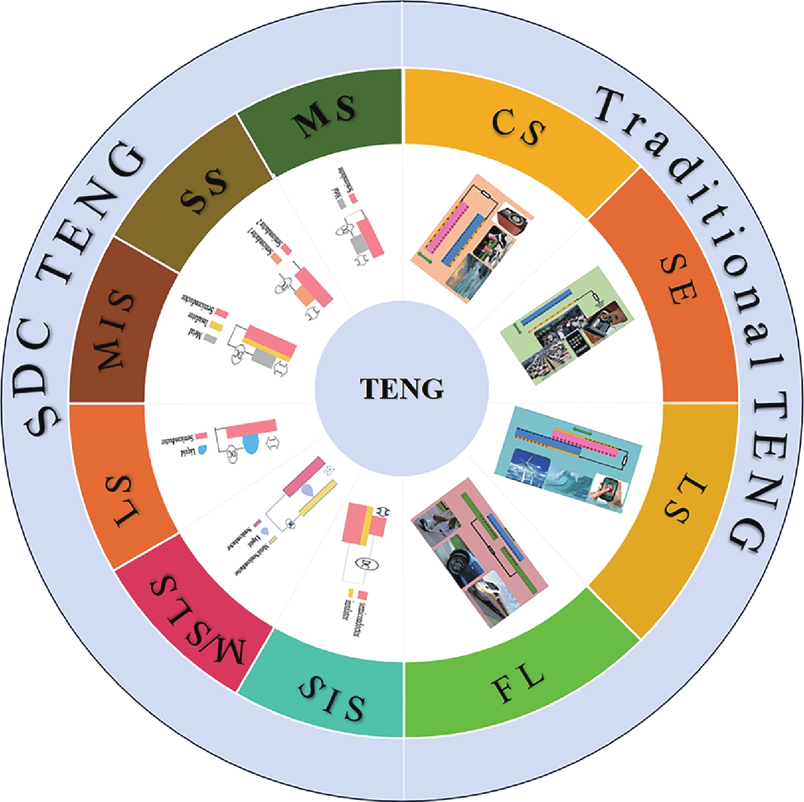
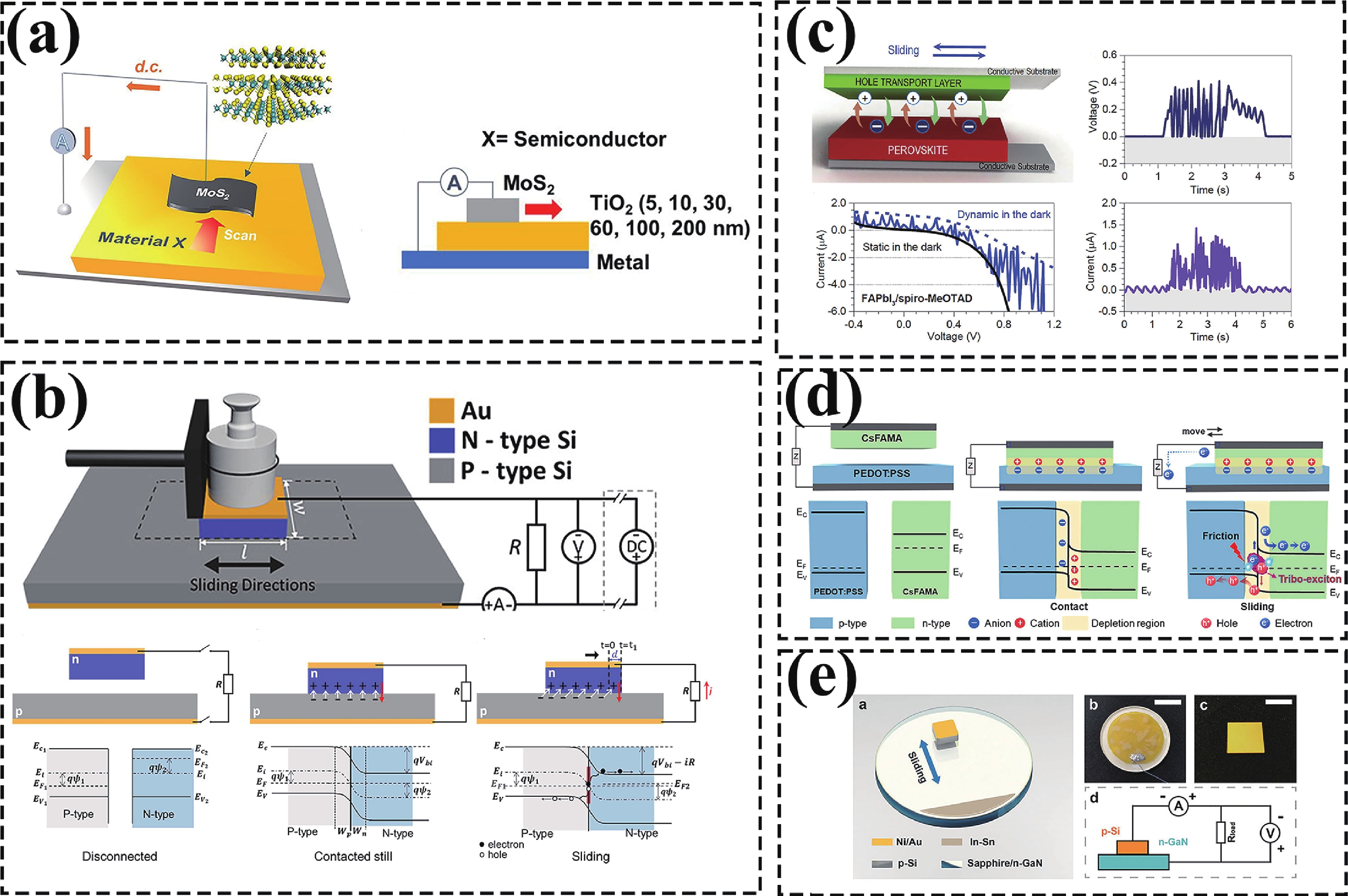
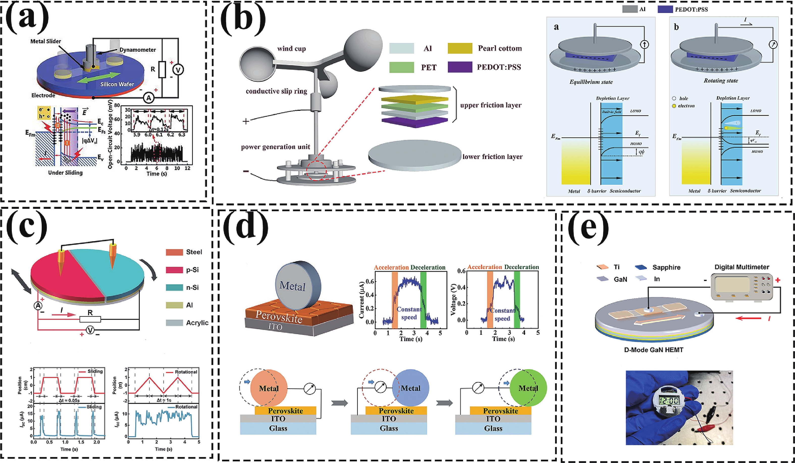
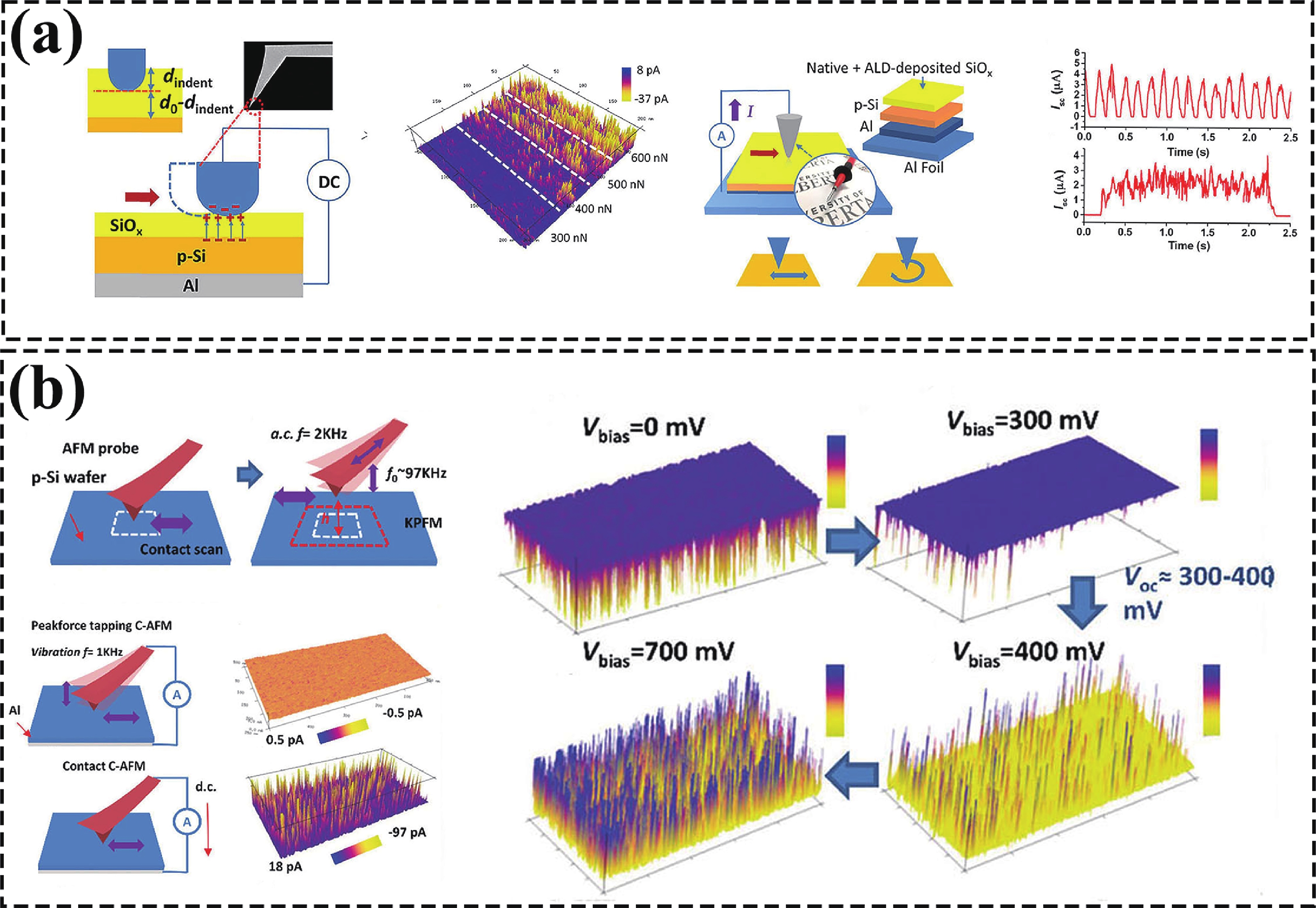
Triboelectric nanogenerator (TENG) utilizing tribovoltaic effect can directly produce direct current with high energy conversion efficiency, which expands their application in semiconductor devices and self-powered systems. This work comprehensively summarizes the recent developments in semiconductor-based direct current TENGs (SDC-TENGs), which hold significant promise for DC energy harvesting technologies and semiconductor systems. First, the tribovoltaic effect is elucidated, and SDC-TENGs are categorized into six types based on different triboelectric structures: metal−semiconductor (M−S), metal−insulator−semiconductor (M−I−S), semiconductor−semiconductor (S−S), semiconductor−insulator−semiconductor (S−I−S), liquid−semiconductor (L−S), and metal/semiconductor−liquid−semiconductor (M/S−L−S) contact devices. Subsequent sections detail the operational mechanisms, strengths, and limitations of each category. Additionally, this paper outlines the enhancement mechanisms of SDC-TENGs providing guidance and recommendations for performance improvement. The conclusion highlights potential application scenarios for various types of SDC-TENGs, outlining the prospective benefits and challenges. SDC-TENG technology is poised to drive revolutionary developments in semiconductor devices and self-powered systems. -
References
[1] Napolitano R, Reinhart W, Gevaudan J P. Smart cities built with smart materials. Science, 2021, 371, 1200 doi: 10.1126/science.abg4254[2] Zhang Z, Wu N, Gong L, et al. An ultrahigh power density and ultralow wear GaN-based tribovoltaic nanogenerator for sliding ball bearing as self-powered wireless sensor node. Adv Mater, 2024, 36, 2310098 doi: 10.1002/adma.202310098[3] Zhou X Y, Li G C, Wu D, et al. Recent advances of cellular stimulation with triboelectric nanogenerators. Exploration, 2023, 3, 20220090 doi: 10.1002/EXP.20220090[4] Wang J, Li S M, Yi F, et al. Sustainably powering wearable electronics solely by biomechanical energy. Nat Commun, 2016, 7, 12744 doi: 10.1038/ncomms12744[5] Xi Y, Tan P C, Li Z, et al. Self−powered wearable IoT sensors as human-machine interfaces. Soft Sci, 2023, 3, 26[6] Zhang Y Z, Gao X Y, Wu Y H, et al. Self−powered technology based on nanogenerators for biomedical applications. Exploration, 2021, 1, 90 doi: 10.1002/EXP.20210152[7] Sriphan S, Charoonsuk T, Maluangnont T, et al. High−performance hybridized composited-based piezoelectric and triboelectric nanogenerators based on BaTiO3/PDMS composite film modified with Ti0.8O2 nanosheets and silver nanopowders cofillers. ACS Appl Energy Mater, 2019, 2, 3840 doi: 10.1021/acsaem.9b00513[8] Jiang T, Pang H, An J, et al. Robust swing−structured triboelectric nanogenerator for efficient blue energy harvesting. Adv Energy Mater, 2020, 10, 2000064 doi: 10.1002/aenm.202000064[9] He W C, Liu W L, Chen J, et al. Boosting output performance of sliding mode triboelectric nanogenerator by charge space-accumulation effect. Nat Commun, 2020, 11, 4277 doi: 10.1038/s41467-020-18086-4[10] Li Q Y, Hu Y W, Yang Q X, et al. A robust constant–voltage DC triboelectric nanogenerator using the ternary dielectric triboelectrification effect. Adv Energy Mater, 2023, 13, 2202921 doi: 10.1002/aenm.202202921[11] Wang J L, Li Y K, Xie Z J, et al. Cylindrical direct–current triboelectric nanogenerator with constant output current. Adv Energy Mater, 2020, 10, 1904227 doi: 10.1002/aenm.201904227[12] Sun D J, Song W Z, Li C L, et al. High−voltage direct current triboelectric nanogenerator based on charge pump and air ionization for electrospinning. Nano Energy, 2022, 101, 107599 doi: 10.1016/j.nanoen.2022.107599[13] Yang P Y, Zhou L L, Gao Y K, et al. Achieving high–performance triboelectric nanogenerator by DC pump strategy. Adv Mater Technol, 2023, 8, 2201957 doi: 10.1002/admt.202201957[14] Yu X T, Zheng H N, Lu Y H, et al. Wind driven semiconductor electricity generator with high direct current output based on a dynamic schottky junction. RSC Adv, 2021, 11, 19106 doi: 10.1039/D1RA02308J[15] Bernardo C P C V, Lameirinhas R A M, de Melo Cunha J P, et al. A revision of the semiconductor theory from history to applications. Discov Appl Sci, 2024, 6, 316 doi: 10.1007/s42452-024-06001-1[16] Yang R Z, Xu R, Dou W J, et al. Semiconductor−based dynamic heterojunctions as an emerging strategy for high direct−current mechanical energy harvesting. Nano Energy, 2021, 83, 105849 doi: 10.1016/j.nanoen.2021.105849[17] Wang Z L. Triboelectric nanogenerators as new energy technology and self-powered sensors-principles, problems and perspectives. Faraday Discuss, 2014, 176, 447 doi: 10.1039/C4FD00159A[18] Chen Y K, Zhang Z, Wang Z Z, et al. Friction-dominated carrier excitation and transport mechanism for GaN-based direct-current triboelectric nanogenerators. ACS Appl Mater, 2022, 14, 24020 doi: 10.1021/acsami.2c03853[19] Zhang Z, Wang Z Z, Chen Y K, et al. Semiconductor contact−electrification−dominated tribovoltaic effect for ultrahigh power generation. Adv Mater, 2022, 34, 2200146 doi: 10.1002/adma.202200146[20] Wang Z L, Wang A C. On the origin of contact−electrification. Mater Today, 2019, 30, 34 doi: 10.1016/j.mattod.2019.05.016[21] Fan F R, Tian Z Q, Wang Z L. Flexible triboelectric generator. Nano Energy, 2012, 1, 328 doi: 10.1016/j.nanoen.2012.01.004[22] Xu C, Yu J R, Huo Z W, et al. Pursuing the tribovoltaic effect for direct-current triboelectric nanogenerators. Energy Environ Sci, 2023, 16, 983 doi: 10.1039/D2EE04019K[23] Xu R, Zhang Q, Wang J Y, et al. Direct current triboelectric cell by sliding an n-type semiconductor on a p-type semiconductor. Nano Energy, 2019, 66, 104185 doi: 10.1016/j.nanoen.2019.104185[24] Liu J, Cheikh M I, Bao R M, et al. Tribo-tunneling DC generator with carbon aerogel/silicon multi-nanocontacts. Adv Electron Mater, 2019, 5, 1900464 doi: 10.1002/aelm.201900464[25] Lu Y H, Feng S R, Shen R J, et al. Tunable dynamic black phosphorus/insulator/si heterojunction direct-current generator based on the hot electron transport. Research, 2019, 2019, 5832382[26] Liu J, Liu F F, Bao R M, et al. Scaled-up direct-current generation in MoS2 multilayer-based moving heterojunctions. ACS Appl Mater, 2019, 11, 35404 doi: 10.1021/acsami.9b09851[27] Xu C, Wang A C, Zou H Y, et al. Raising the working temperature of a triboelectric nanogenerator by quenching down electron thermionic emission in contact-electrification. Adv Mater, 2018, 30, 1803968 doi: 10.1002/adma.201803968[28] Xu C, Zi Y L, Wang A C, et al. On the electron-transfer mechanism in the contact-electrification effect. Adv Mater, 2018, 30, 1706790 doi: 10.1002/adma.201706790[29] Ma C Q, Kim B, Kim S W, et al. Dynamic halide perovskite heterojunction generates direct current. Energy Environ Sci, 2021, 14, 374 doi: 10.1039/D0EE03487H[30] Lee Y S, Jeon S, Kim D, et al. High performance direct current-generating triboelectric nanogenerators based on tribovoltaic p-n junction with ChCl-passivated CsFAMA perovskite. Nano Energy, 2023, 106, 108066 doi: 10.1016/j.nanoen.2022.108066[31] Wang Z Z, Zhang Z, Chen Y K, et al. Achieving an ultrahigh direct-current voltage of 130 V by semiconductor heterojunction power generation based on the tribovoltaic effect. Energy Environ Sci, 2022, 15, 2366 doi: 10.1039/D2EE00180B[32] Zhang Z, Jiang D D, Zhao J Q, et al. Tribovoltaic effect on metal–semiconductor interface for direct-current low-impedance triboelectric nanogenerators. Adv Energy Mater, 2020, 10, 1903713 doi: 10.1002/aenm.201903713[33] You Z Y, Wang X, Lu F Q, et al. An organic semiconductor/metal Schottky heterojunction based direct current triboelectric nanogenerator windmill for wind energy harvesting. Nano Energy, 2023, 109, 108302 doi: 10.1016/j.nanoen.2023.108302[34] Dong S C, Bu T Z, Wang Z Z, et al. Freestanding–mode tribovoltaic nanogenerator for harvesting sliding and rotational mechanical energy. Adv Energy Mater, 2023, 13, 2300079 doi: 10.1002/aenm.202300079[35] Yuan H, Xiao Z X, Wan J X, et al. A rolling-mode Al/CsPbBr3 schottky junction direct-current triboelectric nanogenerator for harvesting mechanical and solar energy. Adv Energy Mater, 2022, 12, 2200550 doi: 10.1002/aenm.202200550[36] Luo Q Q, Xiao K, Li M, et al. Metal−semiconductor direct-current triboelectric nanogenerator based on depletion mode u-GaN/AlGaN/AlN/GaN HEMT. Appl Phys Lett, 2023, 123, 063902 doi: 10.1063/5.0158240[37] Liu J, Miao M M, Jiang K R, et al. Sustained electron tunneling at unbiased metal−insulator−semiconductor triboelectric contacts. Nano Energy, 2018, 48, 320 doi: 10.1016/j.nanoen.2018.03.068[38] Alexe M, Hesse D. Tip-enhanced photovoltaic effects in bismuth ferrite. Nat Commun, 2011, 2, 256 doi: 10.1038/ncomms1261[39] Zhu G, Lin ZH, Jing Q, et al. Toward large-scale energy harvesting by a nanoparticle-enhanced triboelectric nanogenerator. Nano Lett, 2013, 13, 847 doi: 10.1021/nl4001053[40] Reid O G, Munechika K, Ginger D S. Space charge limited current measurements on conjugated polymer films using conductive atomic force microscopy. Nano Lett, 2008, 8, 1602 doi: 10.1021/nl080155l[41] Liu J, Jiang K R, Nguyen L, et al. Interfacial friction-induced electronic excitation mechanism for tribo-tunneling current generation. Mater Horiz, 2019, 6, 1020 doi: 10.1039/C8MH01259H[42] Li X Q, Lin S S, Lin X, et al. Graphene/h-BN/GaAs sandwich diode as solar cell and photodetector. Opt Express, 2016, 24, 134 doi: 10.1364/OE.24.000134[43] Wang X M, Qi L Q, Yang H H, et al. Stretchable synaptic transistors based on the field effect for flexible neuromorphic electronics. Soft Sci, 2023, 15[44] Cai X, Xiao Y, Zhang B W, et al. Surface control and electrical tuning of MXene electrode for flexible self–powered human–machine interaction. Adv Funct Mater, 2023, 33, 2304456 doi: 10.1002/adfm.202304456[45] Lin S S, Lu Y H, Feng S R, et al. A high current density direct-current generator based on a moving van der waals schottky diode. Adv Mater, 2019, 31, 1804398 doi: 10.1002/adma.201804398[46] Zheng M L, Lin S Q, Xu L, et al. Scanning probing of the tribovoltaic effect at the sliding interface of two semiconductors. Adv Mater, 2020, 32, 2000928 doi: 10.1002/adma.202000928[47] Zhou L L, Liu D, Zhao Z H, et al. Simultaneously enhancing power density and durability of sliding–mode triboelectric nanogenerator via interface liquid lubrication. Adv Energy Mater, 2020, 10, 2002920 doi: 10.1002/aenm.202002920[48] Lin S Q, Chen X Y, Wang Z L. Contact electrification at the liquid-solid interface. Chem Rev, 2022, 122, 5209 doi: 10.1021/acs.chemrev.1c00176[49] Chen Y, Xie B, Long J Y, et al. Interfacial laser-induced graphene enabling high-performance liquid−solid triboelectric nanogenerator. Adv Mater, 2021, 33, 2104290 doi: 10.1002/adma.202104290[50] Ghosh S, Sood A, Ramaswamy S, et al. Flow-induced voltage and current generation in carbon nanotubes. Phys Rev B, 2004, 70, 205423 doi: 10.1103/PhysRevB.70.205423[51] Král P, Shapiro M. Nanotube electron erag in flowing liquids. Phys Rev Lett, 2001, 86, 131 doi: 10.1103/PhysRevLett.86.131[52] Yin J, Li X M, Yu J, et al. Generating electricity by moving a droplet of ionic liquid along graphene. Nat Nanotechnol, 2014, 9, 378 doi: 10.1038/nnano.2014.56[53] Xue G B, Xu Y, Ding T P, et al. Water-evaporation-induced electricity with nanostructured carbon materials. Nat Nanotechnol, 2017, 12, 317 doi: 10.1038/nnano.2016.300[54] Lu Y H, Yan Y F, Yu X T, et al. Polarized water driven dynamic pn junction-based direct-current generator. Research, 2021, 2021, 7505638[55] Xiang L M, Zhang P, Liu C R, et al. Conductance and configuration of molecular gold-water-gold junctions under electric fields. Matter, 2020, 3, 166 doi: 10.1016/j.matt.2020.03.023[56] Wei K Q, Sun D J, Liu M N, et al. Direct current nanogenerator based on tribovoltaic effect at WS2 semiconductor interface. ACS Appl Nano Mater, 2024, 7, 1748[57] Song Y D, Wang N, Wang Y H, et al. Direct current triboelectric nanogenerators. Adv Energy Mater, 2020, 10, 2002756 doi: 10.1002/aenm.202002756[58] Wang Z L. Triboelectric nanogenerators as new energy technology for self-powered systems and as active mechanical and chemical sensors. ACS Nano, 2013, 7, 9533 doi: 10.1021/nn404614z[59] Chen J, Yang J, Li Z L, et al. Networks of triboelectric nanogenerators for harvesting water wave energy: a potential approach toward blue energy. ACS Nano, 2015, 9, 3324 doi: 10.1021/acsnano.5b00534[60] Park J Y, Salmeron M. Fundamental aspects of energy dissipation in friction. Chem Rev, 2014, 114, 677 doi: 10.1021/cr200431y[61] Lu Y H, Gao Q Y, Yu X T, et al. Interfacial built-in electric field-driven direct current generator based on dynamic silicon homojunction. Research, 2020, 5714754[62] Benner M, Yang R Z, Lin L Q, et al. Mechanism of in-plane and out-of-plane tribovoltaic direct-current transport with a metal/oxide/metal dynamic heterojunction. ACS Appl Mater, 2022, 14, 2968 doi: 10.1021/acsami.1c22438[63] Chen Y R, Zhang H, Xu C H, et al. Characteristic of solid-ferrofluid triboelectric nanogenerator for ultra-low-frequency vibration energy harvesting. Nano Energy, 2023, 111, 108395 doi: 10.1016/j.nanoen.2023.108395[64] Wang Z Z, Gong L K, Dong S C, et al. A humidity-enhanced silicon-based semiconductor tribovoltaic direct-current nanogenerator. J Mater Chem A, 2022, 10, 25230 doi: 10.1039/D2TA07637C[65] Lin S Q, Chen X Y, Wang Z L. The tribovoltaic effect and electron transfer at a liquid−semiconductor interface. Nano Energy, 2020, 76, 105070 doi: 10.1016/j.nanoen.2020.105070[66] Liu J, Goswami A, Jiang K R, et al. Direct-current triboelectricity generation by a sliding Schottky nanocontact on MoS2 multilayers. Nat Nanotech, 2018, 13, 112 doi: 10.1038/s41565-017-0019-5[67] Zhang Z, Gong L K, Luan R F, et al. Tribovoltaic effect: Origin, interface, characteristic, mechanism & application. Adv Sci, 2024, 11, 2305460 doi: 10.1002/advs.202305460[68] Dai L C, Liu J, Han C, et al. Influence of electronic transmission on the electrical transport properties in metal–semiconductor contacts. Phys Status Solidi A, 2015, 212, 2791 doi: 10.1002/pssa.201532222[69] Imada M, Fujimori A, Tokura Y. Metal-insulator transitions. Rev Mod Phys, 1998, 70, 1039 doi: 10.1103/RevModPhys.70.1039[70] Sohn A, Kim H, Kim D W, et al. Evolution of local work function in epitaxial VO2 thin films spanning the metal-insulator transition. Appl Phys Lett, 2012, 101, 191605 doi: 10.1063/1.4766292[71] Tselev A, Luk’yanchuk I A, Ivanov I N, et al. Symmetry relationship and strain-induced transitions between insulating M1 and M2 and metallic R phases of vanadium dioxide. Nano Lett, 2010, 10, 4409 doi: 10.1021/nl1020443[72] Wentzcovitch R M, Schulz W W, Allen P B. VO2: Peierls or mott-hubbard? a view from band theory. Phys Rev Lett, 1994, 72, 3389 doi: 10.1103/PhysRevLett.72.3389[73] Jördens R, Strohmaier N, Günter K, et al. A Mott insulator of Fermionic atoms in an optical lattice. Nature, 2008, 455, 204 doi: 10.1038/nature07244[74] Zohar A, Kulbak M, Levine I, et al. What limits the open-circuit voltage of bromide perovskite-based solar cells? ACS Energy Lett, 2019, 4, 1 doi: 10.1021/acsenergylett.8b01920[75] Liao Z M, Liu K J, Zhang J M, et al. Effect of surface states on electron transport in individual ZnO nanowires. Phys Lett A, 2007, 367, 207 doi: 10.1016/j.physleta.2007.03.006[76] Liu L T, Kong L G, Li Q Y, et al. Transferred van der waals metal electrodes for sub-1-nm MoS2 vertical transistors. Nat Electron, 2021, 4, 342 doi: 10.1038/s41928-021-00566-0[77] Yang R Z, He Z H, Lin S Q, et al. Tunable tribovoltaic effect via metal-insulator transition. Nano Lett, 2022, 22, 9084 doi: 10.1021/acs.nanolett.2c03481[78] O’Callahan B T, Jones A C, Hyung Park J, et al. Inhomogeneity of the ultrafast insulator-to-metal transition dynamics of VO2. Nat Commun, 2015, 6, 6849 doi: 10.1038/ncomms7849[79] Lysenko S, Rua A J, Vikhnin V, et al. Light-induced ultrafast phase transitions in VO2 thin film. Appl Surf Sci, 2006, 252, 5512 doi: 10.1016/j.apsusc.2005.12.137[80] Lysenko S, Rúa A, Vikhnin V, et al. Insulator-to-metal phase transition and recovery processes in VO2 thin films after femtosecond laser excitation. Phys Rev B, 2007, 76, 035104 doi: 10.1103/PhysRevB.76.035104[81] Dong K, Tang W. Nanogenerators and micro/nano energy harvesting. Sci Sin-Tech, 2023, 53, 953 doi: 10.1360/SST-2023-0034[82] Chen J, Zhu G, Yang W Q, et al. Harmonic-resonator-based triboelectric nanogenerator as a sustainable power source and a self-powered active vibration sensor. Adv Mater, 2013, 25, 6094 doi: 10.1002/adma.201302397[83] Zhu G, Su Y J, Bai P, et al. Harvesting water wave energy by asymmetric screening of electrostatic charges on a nanostructured hydrophobic thin-film surface. ACS Nano, 2014, 8, 6031 doi: 10.1021/nn5012732[84] Zheng L, Lin Z H, Cheng G, et al. Silicon-based hybrid cell for harvesting solar energy and raindrop electrostatic energy. Nano Energy, 2014, 9, 291 doi: 10.1016/j.nanoen.2014.07.024[85] Shang W Y, Gu G Q, Zhang W H, et al. Rotational pulsed triboelectric nanogenerators integrated with synchronously triggered mechanical switches for high efficiency self-powered systems. Nano Energy, 2021, 82, 105725 doi: 10.1016/j.nanoen.2020.105725[86] Liu D, Li C Y, Chen P F, et al. Sustainable long-term and wide-area environment monitoring network based on distributed self-powered wireless sensing nodes. Adv Energy Mater, 2023, 13, 2202691 doi: 10.1002/aenm.202202691[87] Zou Y J, Libanori A, Xu J, et al. Triboelectric nanogenerator enabled smart shoes for wearable electricity generation. Research, 2020, 7158953[88] Niu S M, Wang X F, Yi F, et al. A universal self-charging system driven by random biomechanical energy for sustainable operation of mobile electronics. Nat Commun, 2015, 6, 8975 doi: 10.1038/ncomms9975[89] Zhang L, Zhang B B, Chen J, et al. Lawn structured triboelectric nanogenerators for scavenging sweeping wind energy on rooftops. Adv Mater, 2016, 28, 1650 doi: 10.1002/adma.201504462[90] Stanford M G, Li J T, Chyan Y, et al. Laser-induced graphene triboelectric nanogenerators. ACS Nano, 2019, 13, 7166 doi: 10.1021/acsnano.9b02596[91] Pu X, Song W X, Liu M M, et al. Wearable power-textiles by integrating fabric triboelectric nanogenerators and fiber-shaped dye-sensitized solar cells. Adv Energy Mater, 2016, 6, 1601048 doi: 10.1002/aenm.201601048[92] Dong C Q, Leber A, Das Gupta T, et al. High-efficiency super-elastic liquid metal based triboelectric fibers and textiles. Nat Commun, 2020, 11, 3537 doi: 10.1038/s41467-020-17345-8[93] Ye C, Yang S, Ren J, et al. Electroassisted core-spun triboelectric nanogenerator fabrics for intellisense and artificial intelligence perception. ACS Nano, 2022, 16, 4415 doi: 10.1021/acsnano.1c10680[94] Sheng F F, Zhang B, Zhang Y H, et al. Ultrastretchable organogel/silicone fiber-helical sensors for self-powered implantable ligament strain monitoring. ACS Nano, 2022, 16, 10958 doi: 10.1021/acsnano.2c03365[95] Zhao X J, Kuang S Y, Wang Z L, et al. Highly adaptive solid-liquid interfacing triboelectric nanogenerator for harvesting diverse water wwave energy. ACS Nano, 2018, 12, 4280 doi: 10.1021/acsnano.7b08716[96] Liu Y Q, Sun N, Liu J W, et al. Integrating a silicon solar cell with a triboelectric nanogenerator via a mutual electrode for harvesting energy from sunlight and raindrops. ACS Nano, 2018, 12, 2893 doi: 10.1021/acsnano.8b00416[97] Liu D, Yin X, Guo H Y, et al. A constant current triboelectric nanogenerator arising from electrostatic breakdown. Sci Adv, 2019, 5, eaav6437 doi: 10.1126/sciadv.aav6437[98] Li S X, Liu D, Zhao Z H, et al. A fully self-powered vibration monitoring system driven by dual-mode triboelectric nanogenerators. ACS Nano, 2020, 14, 2475 doi: 10.1021/acsnano.9b10142 -
Proportional views


