


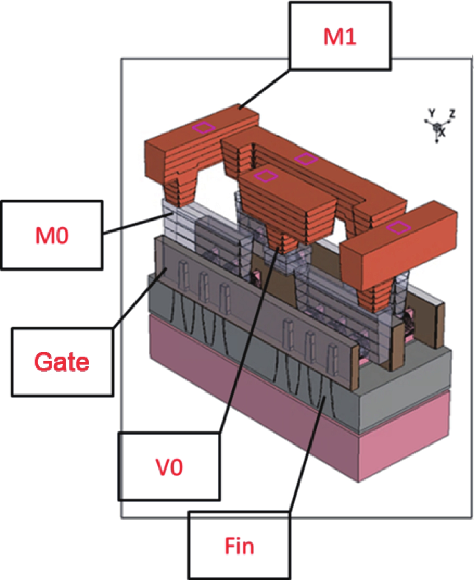
Fig. 1.
(Color online) Schematic diagram of TCAD 14 nm FinFET inverter unit structure.
ARTICLES
Yafen Yang1, 2, Hang Xu1, , Tianyang Feng1, Jianbin Guo1 and David Wei Zhang1, 2
Corresponding author: Hang Xu, hang_xu@fudan.edu.cn
Abstract: The advanced fin-shaped field-effect transistor (FinFET) technology offers higher integration density and stronger channel control capabilities, however, more complex process effects are also introduced which have significant influence on device performance. To address these issues, we complete a design-technology co-optimization (DTCO) focused on FinFET, including both process-induced effect during gate formation and corresponding digital unit optimization design. The 14 nm FinFET complementary metal oxide semiconductor (CMOS) technology is used to illustrate the sensitivity of transistor performance to process-induced effect, specifically the poly pitch effect (PPE) and cut poly effect (CPE). Predictive technology computer aided design (TCAD) simulations have been carried out to evaluate the transistor performance in advance. Based on the results, optimizations in digital unit design is proposed. Fall delay of the digital unit inverter is decreased by 0.7%, and the rise delay is decreased by 2.1%. For multiple selector (MUX2NV), the delay decreases by 4.64% for rise and 3.56% for drop, respectively.
Key words: FinFET, TCAD, process-induced effect, digital unit optimization design
| [1] |
Yeric G, Cline B, Sinha S, et al. The past present and future of design-technology co-optimization. Proceedings of the IEEE 2013 Custom Integrated Circuits Conference, 2013, 1 doi: 10.1109/CICC.2013.6658476
|
| [2] |
Jhaveri T, Rovner V, Liebmann L, et al. Co-optimization of circuits, layout and lithography for predictive technology scaling beyond gratings. IEEE Transactions on Computer-Aided Design of Integrated Circuits and Systems, 2010, 29, 509 doi: 10.1109/TCAD.2010.2042882
|
| [3] |
Karner M, Rzepa G, Schleich C, et al. An efficient and accurate DTCO simulation framework for reliability and variability-aware explorations of FinFETs, nanosheets, and beyond. 2024 8th IEEE Electron Devices Technology & Manufacturing Conference (EDTM), 2024, 1 doi: 10.1109/EDTM58488.2024.10511441
|
| [4] |
Kim T. Recent research in design and technology co-optimization with multi-bit flip-flops. 2024 IEEE 67th International Midwest Symposium on Circuits and Systems (MWSCAS), 2024, 33 doi: 10.1109/MWSCAS60917.2024.10658994
|
| [5] |
Kim T. Challenges on design and technology co-optimization: design automation perspective. 2023 IEEE 66th International Midwest Symposium on Circuits and Systems (MWSCAS), 2023, 212 doi: 10.1109/MWSCAS57524.2023.10405868
|
| [6] |
Kang C Y, Baek R H, Kim T W, et al. Comprehensive layout and process optimization study of Si and III-V technology for sub-7nm node. 2013 IEEE International Electron Devices Meeting, 2013, 5.3.1 doi: 10.1109/IEDM.2013.6724566
|
| [7] |
Myung S, Shin D, Kim K, et al. A new industry standard compact model integrating TCAD into SPICE. 2024 IEEE Symposium on VLSI Technology and Circuits (VLSI Technology and Circuits), 2024, 1 doi: 10.1109/VLSITechnologyandCir46783.2024.10631456
|
| [8] |
Ghaida R S, Agarwal K B, Nassif S R, et al. Layout decomposition and legalization for double-patterning technology. IEEE Transactions on Computer-Aided Design of Integrated Circuits and Systems, 2013, 32, 202 doi: 10.1109/TCAD.2012.2232710
|
| [9] |
Huynh K, Saltin J, Han J, et al. Study of layout dependent radiation hardness of FinFET SRAM using full domain 3D TCAD simulation. 2019 IEEE SOI-3D-Subthreshold Microelectronics Technology Unified Conference (S3S), 2019, 1 doi: 10.1109/S3S46989.2019.9320706
|
| [10] |
Yang L, Cui M, Ma J, et al. Advanced spice modeling for 65nm CMOS technology. 2008 9th International Conference on Solid-State and Integrated-Circuit Technology, 2008, 436 doi: 10.1109/ICSICT.2008.4734568
|
| [11] |
Sirisantana N, Wei L, Roy K. High-performance low-power CMOS circuits using multiple channel length and multiple oxide thickness. Proceedings 2000 International Conference on Computer Design, 2000, 227 doi: 10.1109/ICCD.2000.878290
|
| [12] |
Bardon M G, Moroz V, Eneman G, et al. Layout-induced stress effects in 14nm & 10nm FinFETs and their impact on performance. 2013 Symposium on VLSI Circuits, 2013, T114
|
| [13] |
Jang D, Bardon M G, Yakimets D, et al. STI and eSiGe source/drain epitaxy induced stress modeling in 28 nm technology with replacement gate (RMG) process. 2013 Proceedings of the European Solid-State Device Research Conference (ESSDERC), 2013, 159 doi: 10.1109/ESSDERC.2013.6818843
|
| [14] |
Hamaguchi M, Nair D, Jaeger D, et al. New layout dependency in high-k/Metal Gate MOSFETs. 2011 International Electron Devices Meeting, 2011, 25.6.1 doi: 10.1109/IEDM.2011.6131614
|
| [15] |
Li Z Y, Wang X J, Jiang Y L. Metal boundary effect mitigation by HKMG thermal process optimization in FinFET integration technology. IEEE Transactions on Electron Devices, 2024, 71, 2335 doi: 10.1109/TED.2024.3370119
|
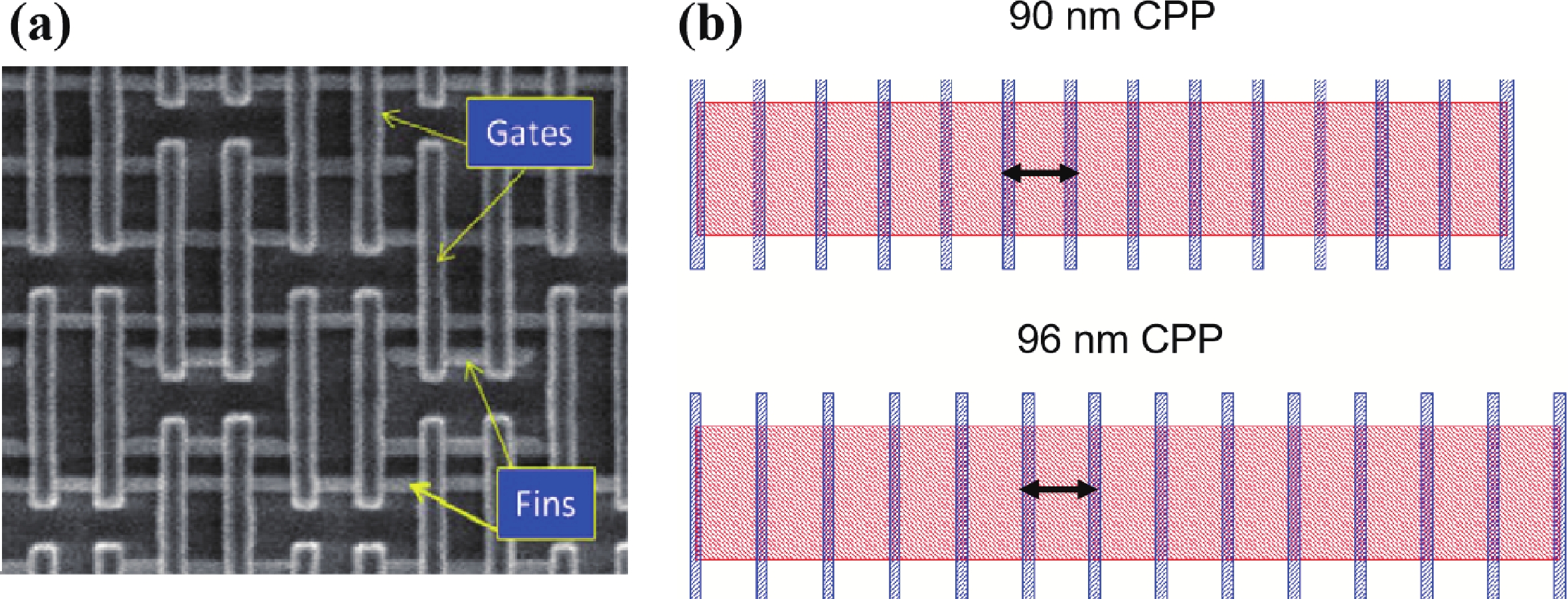

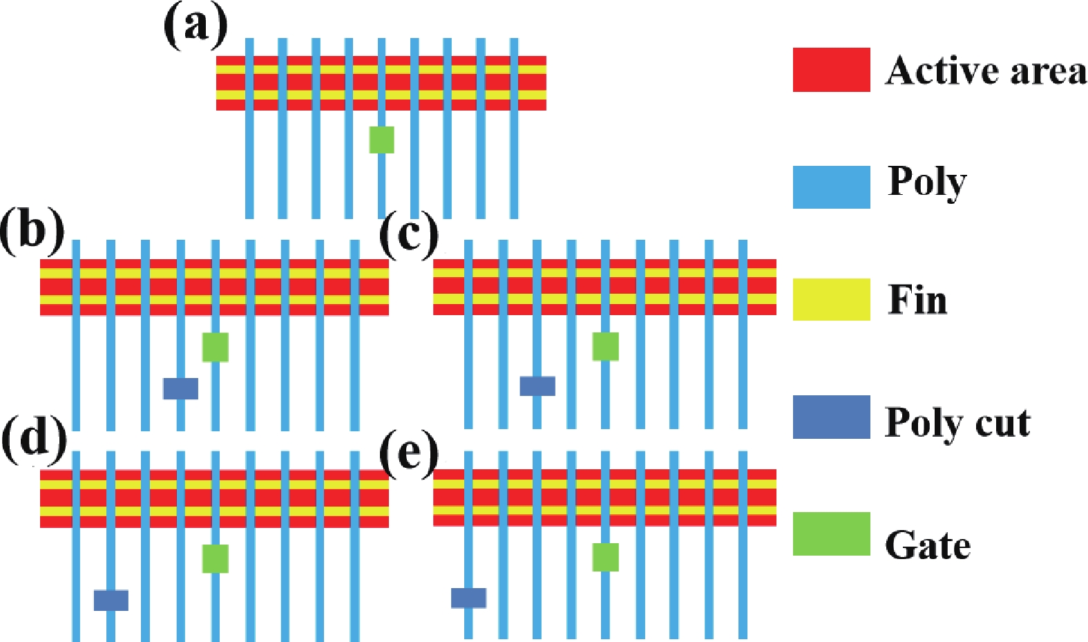
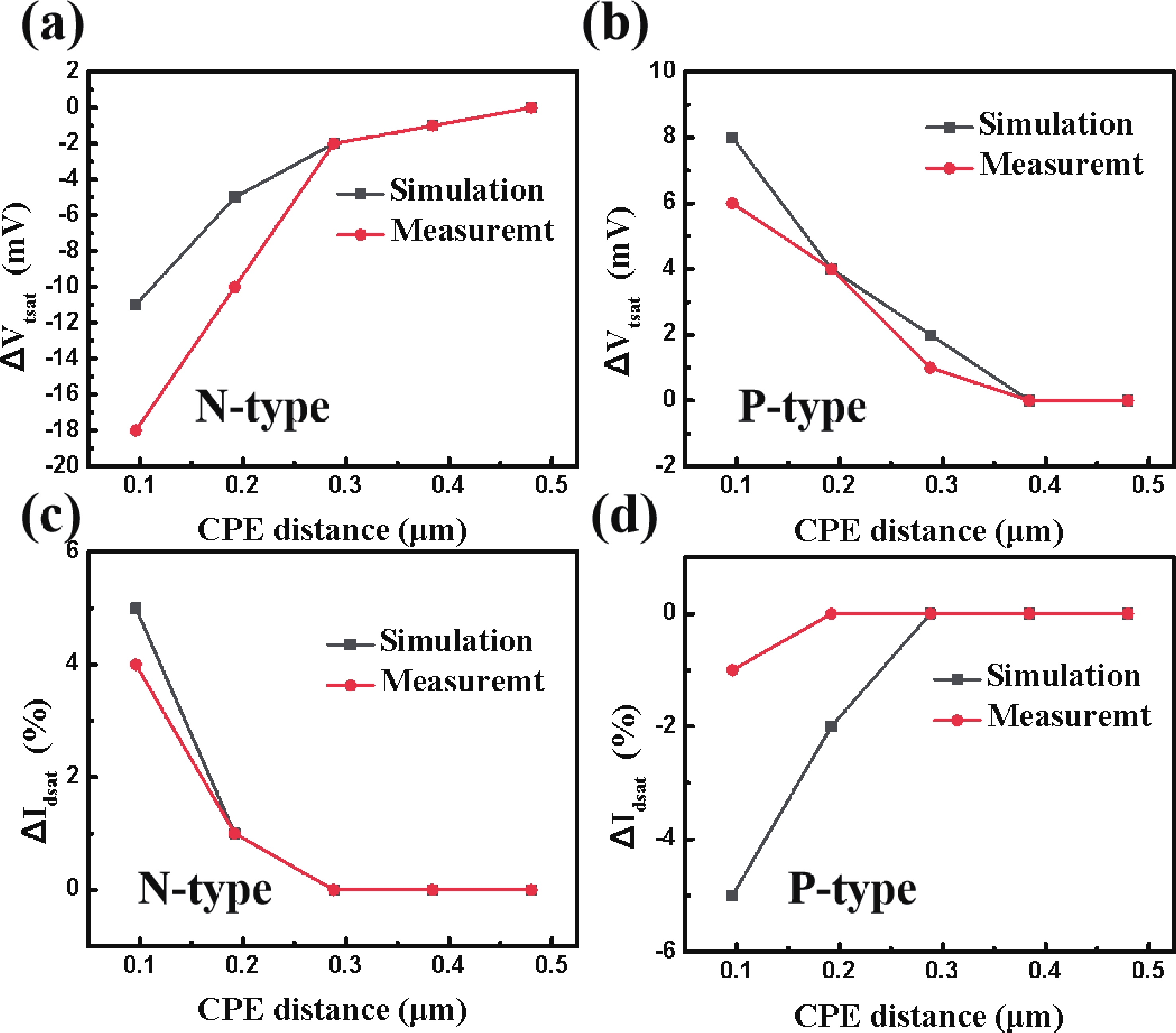
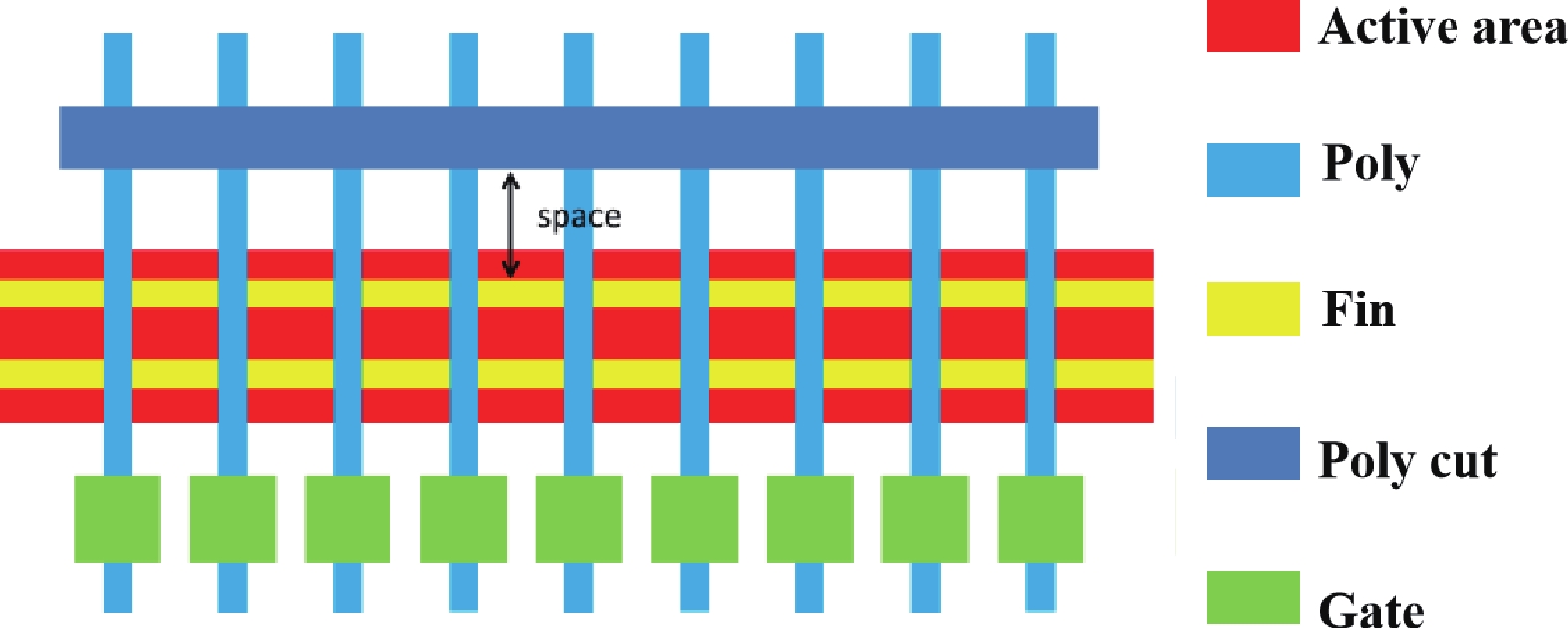
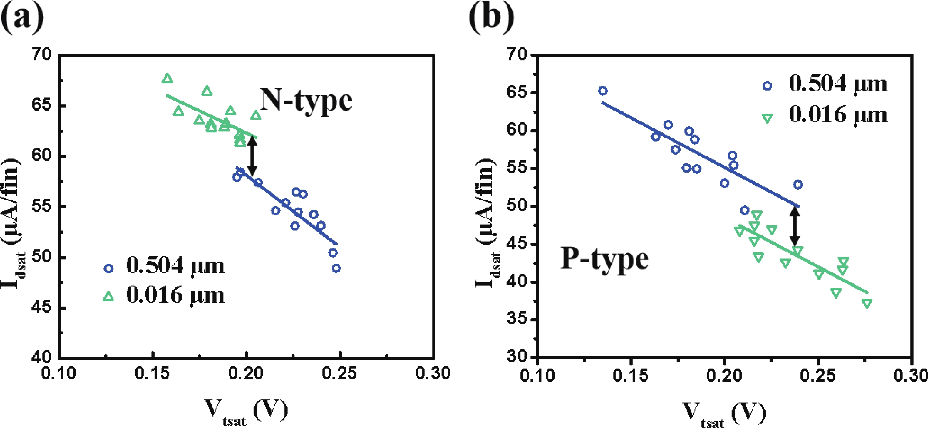
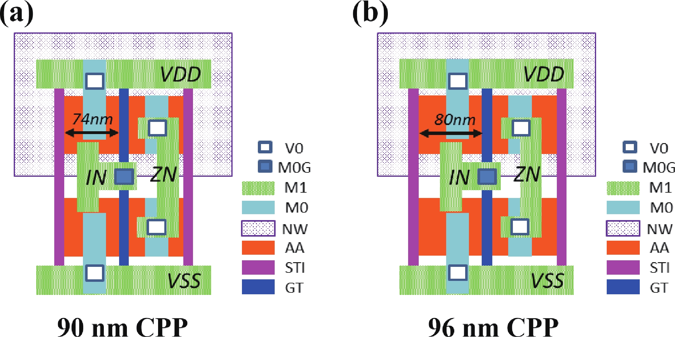
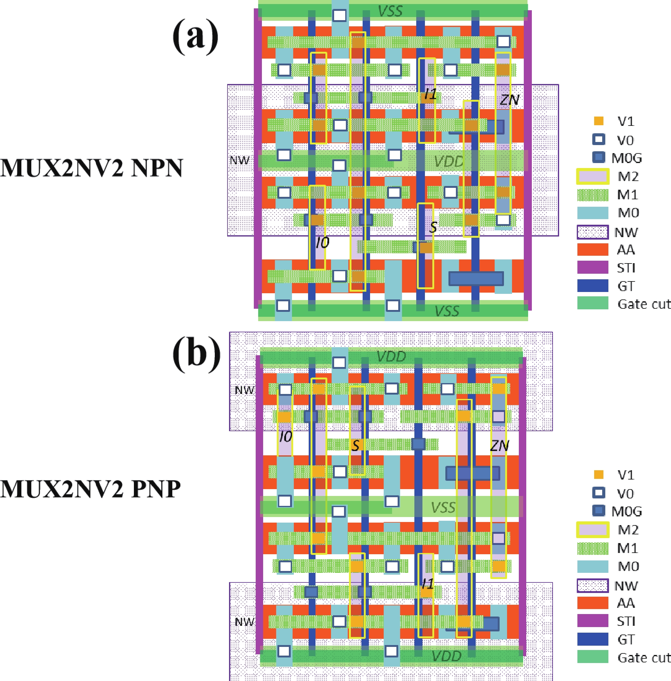
Table 1. Speed comparison of inverter optimized by PPE.
| Digital unit type | Fall delay | Rise delay | Average |
| INV1 (CPP90) (ps) | 9.12 | 8.66 | 8.89 |
| INV2 (CPP96) (ps) | 9.06 | 8.48 | 8.77 |
| Diff (%) | −0.7 | −2.1 | −1.3 |
 DownLoad: CSV
Table 2. Speed comparison of MUX2NV2 optimized by CPE.
| Digital unit type | Fall delay | Rise delay |
| MUX2NV2_1 (ps) | 9.12 | 8.66 |
| MUX2NV2_2 (ps) | 9.06 | 8.48 |
| Diff (%) | −4.64 | −3.56 |
DownLoad: CSV
| [1] |
Yeric G, Cline B, Sinha S, et al. The past present and future of design-technology co-optimization. Proceedings of the IEEE 2013 Custom Integrated Circuits Conference, 2013, 1 doi: 10.1109/CICC.2013.6658476
|
| [2] |
Jhaveri T, Rovner V, Liebmann L, et al. Co-optimization of circuits, layout and lithography for predictive technology scaling beyond gratings. IEEE Transactions on Computer-Aided Design of Integrated Circuits and Systems, 2010, 29, 509 doi: 10.1109/TCAD.2010.2042882
|
| [3] |
Karner M, Rzepa G, Schleich C, et al. An efficient and accurate DTCO simulation framework for reliability and variability-aware explorations of FinFETs, nanosheets, and beyond. 2024 8th IEEE Electron Devices Technology & Manufacturing Conference (EDTM), 2024, 1 doi: 10.1109/EDTM58488.2024.10511441
|
| [4] |
Kim T. Recent research in design and technology co-optimization with multi-bit flip-flops. 2024 IEEE 67th International Midwest Symposium on Circuits and Systems (MWSCAS), 2024, 33 doi: 10.1109/MWSCAS60917.2024.10658994
|
| [5] |
Kim T. Challenges on design and technology co-optimization: design automation perspective. 2023 IEEE 66th International Midwest Symposium on Circuits and Systems (MWSCAS), 2023, 212 doi: 10.1109/MWSCAS57524.2023.10405868
|
| [6] |
Kang C Y, Baek R H, Kim T W, et al. Comprehensive layout and process optimization study of Si and III-V technology for sub-7nm node. 2013 IEEE International Electron Devices Meeting, 2013, 5.3.1 doi: 10.1109/IEDM.2013.6724566
|
| [7] |
Myung S, Shin D, Kim K, et al. A new industry standard compact model integrating TCAD into SPICE. 2024 IEEE Symposium on VLSI Technology and Circuits (VLSI Technology and Circuits), 2024, 1 doi: 10.1109/VLSITechnologyandCir46783.2024.10631456
|
| [8] |
Ghaida R S, Agarwal K B, Nassif S R, et al. Layout decomposition and legalization for double-patterning technology. IEEE Transactions on Computer-Aided Design of Integrated Circuits and Systems, 2013, 32, 202 doi: 10.1109/TCAD.2012.2232710
|
| [9] |
Huynh K, Saltin J, Han J, et al. Study of layout dependent radiation hardness of FinFET SRAM using full domain 3D TCAD simulation. 2019 IEEE SOI-3D-Subthreshold Microelectronics Technology Unified Conference (S3S), 2019, 1 doi: 10.1109/S3S46989.2019.9320706
|
| [10] |
Yang L, Cui M, Ma J, et al. Advanced spice modeling for 65nm CMOS technology. 2008 9th International Conference on Solid-State and Integrated-Circuit Technology, 2008, 436 doi: 10.1109/ICSICT.2008.4734568
|
| [11] |
Sirisantana N, Wei L, Roy K. High-performance low-power CMOS circuits using multiple channel length and multiple oxide thickness. Proceedings 2000 International Conference on Computer Design, 2000, 227 doi: 10.1109/ICCD.2000.878290
|
| [12] |
Bardon M G, Moroz V, Eneman G, et al. Layout-induced stress effects in 14nm & 10nm FinFETs and their impact on performance. 2013 Symposium on VLSI Circuits, 2013, T114
|
| [13] |
Jang D, Bardon M G, Yakimets D, et al. STI and eSiGe source/drain epitaxy induced stress modeling in 28 nm technology with replacement gate (RMG) process. 2013 Proceedings of the European Solid-State Device Research Conference (ESSDERC), 2013, 159 doi: 10.1109/ESSDERC.2013.6818843
|
| [14] |
Hamaguchi M, Nair D, Jaeger D, et al. New layout dependency in high-k/Metal Gate MOSFETs. 2011 International Electron Devices Meeting, 2011, 25.6.1 doi: 10.1109/IEDM.2011.6131614
|
| [15] |
Li Z Y, Wang X J, Jiang Y L. Metal boundary effect mitigation by HKMG thermal process optimization in FinFET integration technology. IEEE Transactions on Electron Devices, 2024, 71, 2335 doi: 10.1109/TED.2024.3370119
|


Article views: 3567 Times PDF downloads: 330 Times Cited by: 0 Times
Received: 22 August 2024 Revised: 11 October 2024 Online: Accepted Manuscript: 24 October 2024Uncorrected proof: 12 November 2024Published: 15 December 2024
| Citation: |
Yafen Yang, Hang Xu, Tianyang Feng, Jianbin Guo, David Wei Zhang. Research on process-induced effect in 14-nm FinFET gate formation and digital unit optimization design[J]. Journal of Semiconductors, 2024, 45(12): 122303. doi: 10.1088/1674-4926/24080032
****
Y F Yang, H Xu, T Y Feng, J B Guo, and D W Zhang, Research on process-induced effect in 14-nm FinFET gate formation and digital unit optimization design[J]. J. Semicond., 2024, 45(12), 122303 doi: 10.1088/1674-4926/24080032

|
 Yafen Yang received her doctoral degree from Fudan University in 2021. She is currently serving as a research assistant at School of Microelectronics in Fudan University, Shanghai. Her research interests include low-power devices, power semiconductor device, silicon-based photoelectric devices and advanced CMOS process manufacturing
 Hang Xu received his bachelor's degree from Northwestern Polytechnical University and doctoral degree from Fudan University in 2024. He is currently serving as a postdoctoral fellow at School of Microelectronics in Fudan University, Shanghai. His research focuses on power semiconductor device, silicon-based photoelectric devices and advanced CMOS process manufacturing
| [1] |
Yeric G, Cline B, Sinha S, et al. The past present and future of design-technology co-optimization. Proceedings of the IEEE 2013 Custom Integrated Circuits Conference, 2013, 1 doi: 10.1109/CICC.2013.6658476
|
| [2] |
Jhaveri T, Rovner V, Liebmann L, et al. Co-optimization of circuits, layout and lithography for predictive technology scaling beyond gratings. IEEE Transactions on Computer-Aided Design of Integrated Circuits and Systems, 2010, 29, 509 doi: 10.1109/TCAD.2010.2042882
|
| [3] |
Karner M, Rzepa G, Schleich C, et al. An efficient and accurate DTCO simulation framework for reliability and variability-aware explorations of FinFETs, nanosheets, and beyond. 2024 8th IEEE Electron Devices Technology & Manufacturing Conference (EDTM), 2024, 1 doi: 10.1109/EDTM58488.2024.10511441
|
| [4] |
Kim T. Recent research in design and technology co-optimization with multi-bit flip-flops. 2024 IEEE 67th International Midwest Symposium on Circuits and Systems (MWSCAS), 2024, 33 doi: 10.1109/MWSCAS60917.2024.10658994
|
| [5] |
Kim T. Challenges on design and technology co-optimization: design automation perspective. 2023 IEEE 66th International Midwest Symposium on Circuits and Systems (MWSCAS), 2023, 212 doi: 10.1109/MWSCAS57524.2023.10405868
|
| [6] |
Kang C Y, Baek R H, Kim T W, et al. Comprehensive layout and process optimization study of Si and III-V technology for sub-7nm node. 2013 IEEE International Electron Devices Meeting, 2013, 5.3.1 doi: 10.1109/IEDM.2013.6724566
|
| [7] |
Myung S, Shin D, Kim K, et al. A new industry standard compact model integrating TCAD into SPICE. 2024 IEEE Symposium on VLSI Technology and Circuits (VLSI Technology and Circuits), 2024, 1 doi: 10.1109/VLSITechnologyandCir46783.2024.10631456
|
| [8] |
Ghaida R S, Agarwal K B, Nassif S R, et al. Layout decomposition and legalization for double-patterning technology. IEEE Transactions on Computer-Aided Design of Integrated Circuits and Systems, 2013, 32, 202 doi: 10.1109/TCAD.2012.2232710
|
| [9] |
Huynh K, Saltin J, Han J, et al. Study of layout dependent radiation hardness of FinFET SRAM using full domain 3D TCAD simulation. 2019 IEEE SOI-3D-Subthreshold Microelectronics Technology Unified Conference (S3S), 2019, 1 doi: 10.1109/S3S46989.2019.9320706
|
| [10] |
Yang L, Cui M, Ma J, et al. Advanced spice modeling for 65nm CMOS technology. 2008 9th International Conference on Solid-State and Integrated-Circuit Technology, 2008, 436 doi: 10.1109/ICSICT.2008.4734568
|
| [11] |
Sirisantana N, Wei L, Roy K. High-performance low-power CMOS circuits using multiple channel length and multiple oxide thickness. Proceedings 2000 International Conference on Computer Design, 2000, 227 doi: 10.1109/ICCD.2000.878290
|
| [12] |
Bardon M G, Moroz V, Eneman G, et al. Layout-induced stress effects in 14nm & 10nm FinFETs and their impact on performance. 2013 Symposium on VLSI Circuits, 2013, T114
|
| [13] |
Jang D, Bardon M G, Yakimets D, et al. STI and eSiGe source/drain epitaxy induced stress modeling in 28 nm technology with replacement gate (RMG) process. 2013 Proceedings of the European Solid-State Device Research Conference (ESSDERC), 2013, 159 doi: 10.1109/ESSDERC.2013.6818843
|
| [14] |
Hamaguchi M, Nair D, Jaeger D, et al. New layout dependency in high-k/Metal Gate MOSFETs. 2011 International Electron Devices Meeting, 2011, 25.6.1 doi: 10.1109/IEDM.2011.6131614
|
| [15] |
Li Z Y, Wang X J, Jiang Y L. Metal boundary effect mitigation by HKMG thermal process optimization in FinFET integration technology. IEEE Transactions on Electron Devices, 2024, 71, 2335 doi: 10.1109/TED.2024.3370119
|

 WeChat ID
Journal of Semiconductors © 2017 All Rights Reserved 京ICP备05085259号-2


