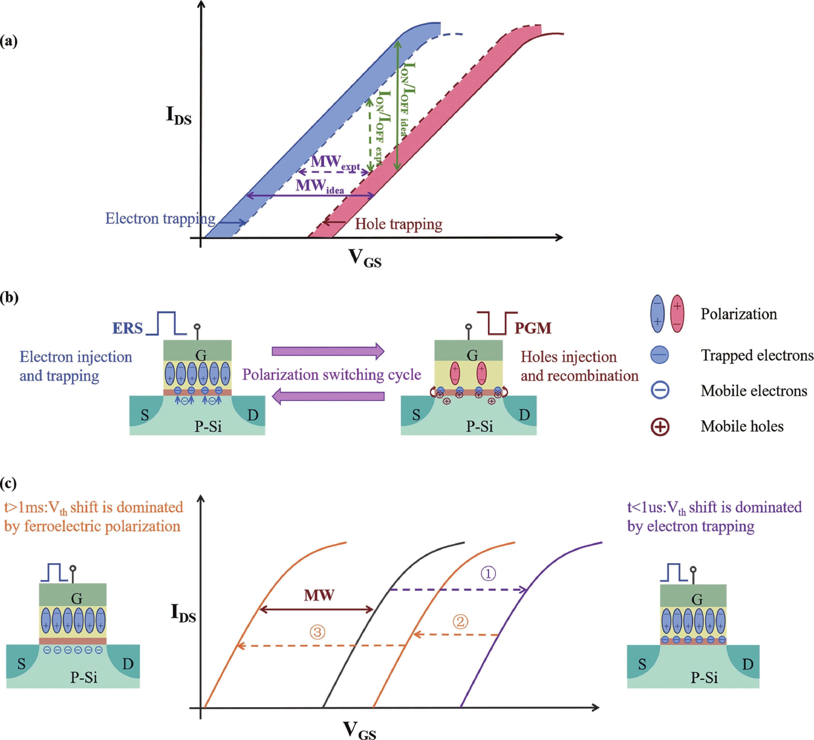
Fig. 1.
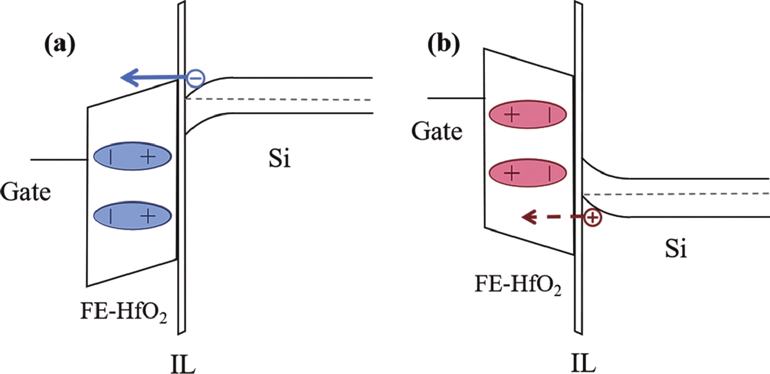
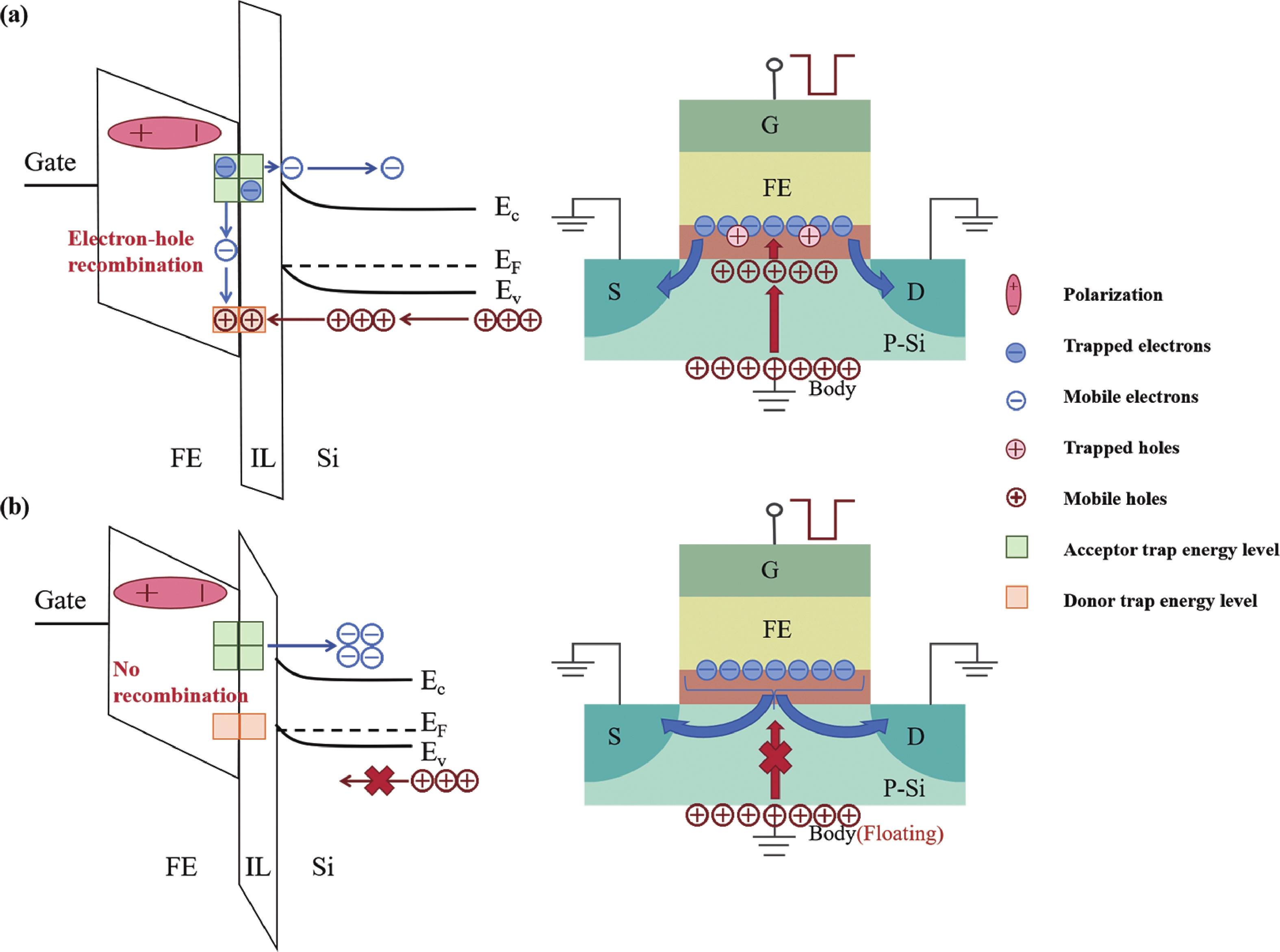
(Color online) Energy band diagrams of Si FeFETs under (a) a positive gate voltage with down-state polarization and (b) a negative gate voltage with up-state polarization[49].
REVIEWS
Yu Song1, 2, 3, Pengfei Jiang1, 2, , Pan Xu1, 2, 3, Xueyang Peng1, 2, 3, Qianqian Wei1, 2, 3, Qingyi Yan1, 2, 3, Wei Wei1, 2, Yuan Wang1, 2, Xiao Long1, 2, Tiancheng Gong1, 2, Yang Yang1, 2, Eskilla Venkata Ramana4 and Qing Luo1, 2,
Corresponding author: Pengfei Jiang, jiangpengfei@ime.ac.cn; Qing Luo, luoqing@ime.ac.cn
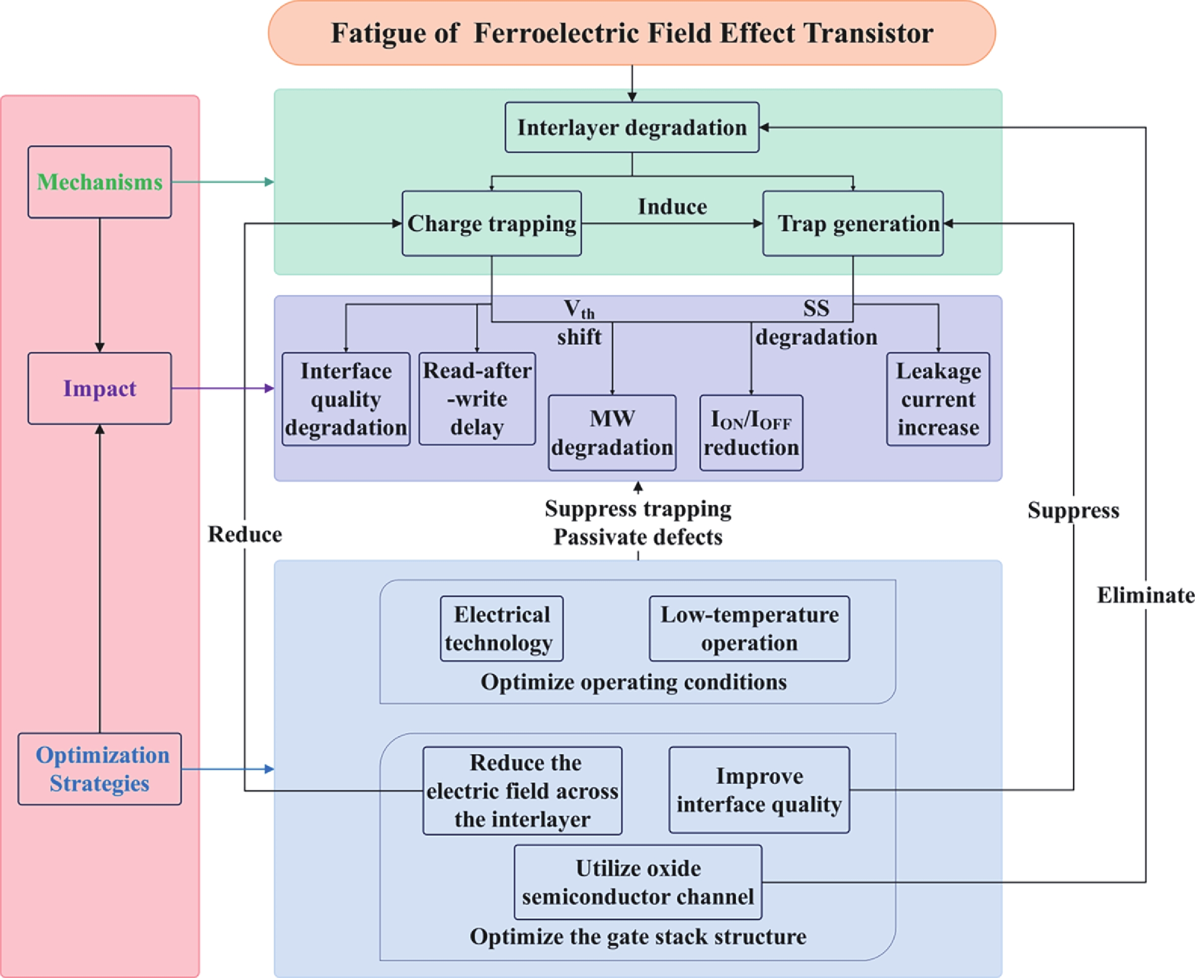
Abstract: The novel HfO2-based ferroelectric field effect transistor (FeFET) is considered a promising candidate for next-generation nonvolatile memory (NVM). However, a series of reliability issues caused by the fatigue effect hinder its further development. Therefore, a comprehensive understanding of the fatigue mechanisms of the device and optimization strategies is essential for its application. The fundamental mechanism of the fatigue effect is attributed to charge trapping and trap generation based on the current studies, and the underlying causes, occurrence locations and specific impacts are analyzed in this review. In particular, the asymmetric trapping/detrapping of electrons and holes, as well as the relationship between the ferroelectric (FE) polarization and charge trapping, are given particular attention. After categorizing and summarizing the current progress, we propose a series of optimization strategies derived based on the fatigue mechanisms.
Key words: FeFET, fatigue, charge trapping, trap generation
| [1] |
Jiao H, Wang X, Wu S, et al. Ferroelectric field effect transistors for electronics and optoelectronics. Appl Phys Rev, 2023, 10(1), 011310 doi: 10.1063/5.0090120
|
| [2] |
Zagni N, Puglisi F M, Pavan P, et al. Reliability of HfO2-based ferroelectric FETs: a critical review of current and future challenges. Proceedings of the IEEE, 2023, 111(2), 158 doi: 10.1109/JPROC.2023.3234607
|
| [3] |
Ajayan J, Mohankumar P, Nirmal D, et al. Ferroelectric field effect transistors (FeFETs): advancements, challenges and exciting prospects for next generation non-volatile memory (NVM) applications. Materials Today Communications, 2023, 35, 105591 doi: 10.1016/j.mtcomm.2023.105591
|
| [4] |
Böscke T, Müller J, Bräuhaus D, et al. Ferroelectricity in hafnium oxide: CMOS compatible ferroelectric field effect transistors. 2011 International electron devices meeting, 2011, 24.5. 1 doi: 10.1109/IEDM.2011.6131606
|
| [5] |
Mulaosmanovic H, Breyer E T, Dünkel S, et al. Ferroelectric field-effect transistors based on HfO2: a review. Nanotechnology, 2021, 32(50), 502002 doi: 10.1088/1361-6528/ac189f
|
| [6] |
Zhang Z, Tian G, Huo J, et al. Recent progress of hafnium oxide-based ferroelectric devices for advanced circuit applications. Sci China Inform Sci, 2023, 66(10), 200405 doi: 10.1007/s11432-023-3780-7
|
| [7] |
Luo Q, Liu M. HfOx based ferroelectric materials and memories. 2021 20th International Workshop on Junction Technology (IWJT), 2021, 1 doi: 10.23919/IWJT52818.2021.9609356
|
| [8] |
Sharma A A, Doyle B, Yoo H J, et al. High speed memory operation in channel-last, back-gated ferroelectric transistors. 2020 IEEE International Electron Devices Meeting (IEDM), 2020, 18.5. 1 doi: 10.1109/IEDM13553.2020.9371940
|
| [9] |
Qin X, Zhong B, Lv S, et al. A zero-voltage-writing artificial nervous system based on biosensor integrated on ferroelectric tunnel junction. Adv Mater, 2024, 2404026 doi: 10.1002/adma.202404026
|
| [10] |
Müller J, Böscke T, Müller S, et al. Ferroelectric hafnium oxide: a CMOS-compatible and highly scalable approach to future ferroelectric memories. 2013 IEEE International Electron Devices Meeting (IEDM), 2013, 10.8. 4 doi: 10.1109/IEDM.2013.6724605
|
| [11] |
Jiang P, Jiang H, Yang Y, et al. A 256 kbit Hf0.5Zr0.5O2-based FeRAM chip with scaled film thickness (sub-8nm), low thermal budget (350 °C), 100% initial chip yield, low power consumption (0.7 pJ/bit at 2V write voltage), and prominent endurance (>1012). 2023 International Electron Devices Meeting (IEDM), 2023, 1 doi: 10.1109/IEDM45741.2023.10413844
|
| [12] |
Wang Y, Yang Y, Jiang P, et al. HfO2-based junctionless FeFET array on FDSOI platform for NAND memory applications. IEEE Electron Device Lett, 2023, 44(6), 943 doi: 10.1109/LED.2023.3267787
|
| [13] |
Jiang P, Xu K, Yu J, et al. Freely switching between ferroelectric and resistive switching in Hf0.5Zr0.5O2 films and its application on high accuracy on-chip deep neural networks. Science China Information Sciences, 2023, 66(2), 122409 doi: 10.1007/s11432-022-3508-7
|
| [14] |
Ma T P, Gong N B. Retention and endurance of FeFET memory cells. 2019 IEEE 11th International Memory Workshop (IMW), 2019, 4-4 doi: 10.1109/IMW.2019.8739726
|
| [15] |
Mikolajick T, Schroeder U, Slesazeck S. The past, the present, and the future of ferroelectric memories. IEEE Transactions on Electron DevicesIEEE Trans Electron Devices, 2020, 67(4), 1434 doi: 10.1109/TED.2020.2976148
|
| [16] |
Shao X, Chai J, Liao M, et al. Comprehensive study of endurance fatigue in the scaled Si FeFET by in-situ Vth measurement and endurance enhancement strategy. 2023 IEEE International Memory Workshop (IMW), 2023, 1 doi: 10.1109/IMW56887.2023.10145966
|
| [17] |
Mulaosmanovic H, Breyer E T, Mikolajick T, et al. Recovery of cycling endurance failure in ferroelectric FETs by self-heating. IEEE Electron Device Lett, 2018, 40(2), 216 doi: 10.1109/LED.2018.2889412
|
| [18] |
Peng H K, Chan C Y, Chen K Y, et al. Enabling large memory window and high reliability for FeFET memory by integrating AlON interfacial layer. Appl Phys Lett, 2021, 118(10), 103503 doi: 10.1063/5.0036824
|
| [19] |
Ali T, Polakowski P, Riedel S, et al. High endurance ferroelectric hafnium oxide-based FeFET memory without retention penalty. IEEE Trans Electron Devices, 2018, 65(9), 3769 doi: 10.1109/TED.2018.2856818
|
| [20] |
Tan A J, Pešić M, Larcher L, et al. Hot electrons as the dominant source of degradation for sub-5nm HZO FeFETs. 2020 IEEE Symposium on VLSI Technology, 2020, 1 doi: 10.1109/VLSITechnology18217.2020.9265067
|
| [21] |
Tan A J, Chatterjee K, Zhou J, et al. Experimental demonstration of a ferroelectric HfO2-based content addressable memory cell. IEEE Electron Device Lett, 2019, 41(2), 240 doi: 10.1109/LED.2019.2963300
|
| [22] |
Ali T, Polakowski P, Kühnel K, et al. A multilevel FeFET memory device based on laminated HSO and HZO ferroelectric layers for high-density storage. 2019 IEEE International Electron Devices Meeting (IEDM), 2019, 28.7.4 doi: 10.1109/IEDM19573.2019.8993642
|
| [23] |
Zhou Y, Liang Z, Luo W, et al. Ferroelectric and interlayer co-optimization with in-depth analysis for high endurance FeFET. 2022 International Electron Devices Meeting (IEDM), 2022, 6.2.4 doi: 10.1109/IEDM45625.2022.10019465
|
| [24] |
Liao C Y, Hsiang K Y, Lou Z F, et al. Endurance > 1011 cycling of 3D GAA nanosheet ferroelectric FET with stacked HfZrO2 to homogenize corner field toward mitigate dead zone for high-density eNVM. 2022 IEEE Symposium on VLSI Technology and Circuits (VLSI Technology and Circuits), 2022, 1 doi: 10.1109/VLSITechnologyandCir46769.2022.9830345
|
| [25] |
Tian F, Zhao S, Xu H, et al. Impact of interlayer and ferroelectric materials on charge trapping during endurance fatigue of FeFET with TiN/HfxZr1-xO2/interlayer/Si (MFIS) gate structure. IEEE Trans Electron Devices, 2021, 68(11), 5872 doi: 10.1109/TED.2021.3114663
|
| [26] |
Lomenzo P D, Takmeel Q, Moghaddam S, et al. Annealing behavior of ferroelectric Si-doped HfO2 thin films. Thin Solid Films, 2016, 615, 139 doi: 10.1016/j.tsf.2016.07.009
|
| [27] |
Pešić M, Fengler F P G, Larcher L, et al. Physical mechanisms behind the field-cycling behavior of HfO2-based ferroelectric capacitors. Adv Funct Mater, 2016, 26(25), 4601 doi: 10.1002/adfm.201600590
|
| [28] |
Yurchuk E, Mueller S, Martin D, et al. Origin of the endurance degradation in the novel HfO2-based 1T ferroelectric non-volatile memories. 2014 IEEE International Reliability Physics Symposium, 2014, 2E.5.5 doi: 10.1109/IRPS.2014.6860603
|
| [29] |
Duhan P, Ali T, Khedgarkar P, et al. Endurance study of silicon-doped hafnium oxide (HSO) and zirconium-doped hafnium oxide (HZO)-based FeFET memory. IEEE Trans Electron Devices, 2023, 70(11), 5645 doi: 10.1109/TED.2023.3316138
|
| [30] |
Jia X, Chai J, Duan J, et al. Investigation of charge trapping induced trap generation in Si FeFET with ferroelectric Hf0.5Zr0.5O2. IEEE Trans Electron Devices, 2024, 71(3), 1845 doi: 10.1109/TED.2024.3351599
|
| [31] |
Shao X, Chai J, Tian F, et al. Investigation of endurance degradation mechanism of Si feFET with HfZrO ferroelectric by an in situ Vth measurement. IEEE Trans Electron Devices, 2023, 70(6), 3043 doi: 10.1109/TED.2023.3265913
|
| [32] |
Gong N, Ma T P. A study of endurance issues in HfO2-based ferroelectric field effect transistors: charge trapping and trap generation. IEEE Electron Device Lett, 2017, 39(1), 15
|
| [33] |
Zeng B, Liao M, Liao J, et al. Program/erase cycling degradation mechanism of HfO2-based FeFET memory devices. IEEE Electron Device Lett, 2019, 40(5), 710 doi: 10.1109/LED.2019.2908084
|
| [34] |
Ichihara R, Higashi Y, Suzuki K, et al. Accurate picture of cycling degradation in HfO2-FeFET based on charge trapping dynamics revealed by fast charge centroid analysis. 2021 IEEE International Electron Devices Meeting (IEDM), 2021, 6.3.4 doi: 10.1109/IEDM19574.2021.9720516
|
| [35] |
Toprasertpong K, Takenaka M, Takagi S. Direct observation of interface charge behaviors in FeFET by quasi-static split CV and Hall techniques: revealing FeFET operation. 2019 IEEE International Electron Devices Meeting (IEDM), 2019, 23.7.4 doi: 10.1109/IEDM19573.2019.8993664
|
| [36] |
Liao M, Xu H, Duan J, et al. Impact of saturated spontaneous polarization on the endurance fatigue of Si FeFET with metal/ferroelectric/interlayer/Si gate structure. IEEE Trans Electron Devices, 2023, 70(8), 4055 doi: 10.1109/TED.2023.3285715
|
| [37] |
Zhao S, Tian F, Xu H, et al. Experimental extraction and simulation of charge trapping during endurance of FeFET with TiN/HfZrO/SiO2/Si (MFIS) gate structure. IEEE Trans Electron Devices, 2022, 69(3), 1561 doi: 10.1109/TED.2021.3139285
|
| [38] |
Bersuker G, Sim J, Park C S, et al. Mechanism of electron trapping and characteristics of traps in HfO2 gate stacks. IEEE Transactions on Device and Materials Reliability, 2007, 7(1), 138 doi: 10.1109/TDMR.2007.897532
|
| [39] |
Heh D, Choi R, Young C D, et al. Fast and slow charge trapping/detrapping processes in high-k nMOSFETs. 2006 IEEE International Integrated Reliability Workshop Final Report, 2006, 120 doi: 10.1109/IRWS.2006.305224
|
| [40] |
Gavartin J, Muñoz Ramo D, Shluger A, et al. Negative oxygen vacancies in HfO2 as charge traps in high-k stacks. Appl Phys Lett, 2006, 89(8), 082908 doi: 10.1063/1.2236466
|
| [41] |
Chowdhury N, Misra D. Charge trapping at deep states in Hf−Silicate based high-k gate dielectrics. J Electrochem Soc, 2006, 154(2), G30 doi: 10.1149/1.2402989
|
| [42] |
Foster A S, Gejo F L, Shluger A, et al. Vacancy and interstitial defects in hafnia. Phys Rev B, 2002, 65(17), 174117 doi: 10.1103/PhysRevB.65.174117
|
| [43] |
Ribes G, Muller M, Bruyere S, et al. Characterization of Vt instability in hafnium based dielectrics by pulse gate voltage techniques [CMOS device applications]. Proceedings of the 30th European Solid-State Circuits Conference (IEEE Cat. No. 04EX850), 2004, 89 doi: 10.1109/ESSDER.2004.1356495
|
| [44] |
Ni K, Sharma P, Zhang J, et al. Critical role of interlayer in Hf0.5Zr0.5O2 ferroelectric FET nonvolatile memory performance. IEEE Trans Electron Devices, 2018, 65(6), 2461 doi: 10.1109/TED.2018.2829122
|
| [45] |
Toprasertpong K, Lin Z, Lee T, et al. Asymmetric polarization response of electrons and holes in Si FeFETs: demonstration of absolute polarization hysteresis loop and inversion hole density over 2×1013 cm−2. 2020 IEEE Symposium on VLSI Technology, 2020, 1 doi: 10.1109/VLSITechnology18217.2020.9265015
|
| [46] |
Yurchuk E, Müller J, Müller S, et al. Charge-trapping phenomena in HfO2-based FeFET-type nonvolatile memories. IEEE Trans Electron Devices, 2016, 63(9), 3501 doi: 10.1109/TED.2016.2588439
|
| [47] |
Li Y, Zhu H, Liu X, et al. Trap characteristics of hafnium oxide-based ferroelectric field-effect transistors measured by using a current transient method. Appl Phys Lett, 2023, 122(11), 112905 doi: 10.1063/5.0137773
|
| [48] |
Tasneem N, Wang Z, Zhao Z, et al. Trap capture and emission dynamics in ferroelectric field-effect transistors and their impact on device operation and reliability. 2021 IEEE International Electron Devices Meeting (IEDM), 2021, 6.1. 4 doi: 10.1109/IEDM19574.2021.9720615
|
| [49] |
Toprasertpong K, Takenaka M, Takagi S. On the strong coupling of polarization and charge trapping in HfO2/Si-based ferroelectric field-effect transistors: overview of device operation and reliability. Appl Phys A, 2022, 128(12), 1114 doi: 10.1007/s00339-022-06212-6
|
| [50] |
Deng S, Zhao Z, Kim Y S, et al. Unraveling the dynamics of charge trapping and de-trapping in ferroelectric FETs. IEEE Trans Electron Devices, 2022, 69(3), 1503 doi: 10.1109/TED.2022.3143485
|
| [51] |
Toprasertpong K, Takenaka M, Takagi S. Understanding memory window of ferroelectric field-effect transistor under coexistence of charge trapping and ferroelectric polarization: violation of linear superposition. Jpn J Appl Phys, 2024, 63(2), 02SP47 doi: 10.35848/1347-4065/ad15e3
|
| [52] |
Ichihara R, Suzuki K, Kusai H, et al. Re-examination of Vth window and reliability in HfO2 FeFET based on the direct extraction of spontaneous polarization and trap charge during memory operation. 2020 IEEE Symposium on VLSI Technology, 2020, 1 doi: 10.1109/VLSITechnology18217.2020.9265055
|
| [53] |
Toprasertpong K, Takenaka M, Takagi S. Memory window in ferroelectric field-effect transistors: analytical approach. IEEE Trans Electron Devices, 2022, 69(12), 7113 doi: 10.1109/TED.2022.3215667
|
| [54] |
Duan J, Zhao S, Tian F, et al. Trap generation in whole gate stacks of FeFET with TiN/Hf0.5Zr0.5O2/SiOx/Si (MFIS) gate structure during endurance fatigue. IEEE Trans Electron Devices, 2022, 69(12), 6547 doi: 10.1109/TED.2022.3215935
|
| [55] |
Chai J, Xu H, Xiang J, et al. First-principles study of oxygen vacancy defects in orthorhombic Hf0.5Zr0.5O2/SiO2/Si gate stack. J Appl Phys, 2022, 132(10), 105301 doi: 10.1063/5.0106750
|
| [56] |
Simoen E, O’Sullivan B, Ronchi N, et al. Low-frequency noise assessment of ferro-electric field-effect transistors with Si-doped HfO2 gate dielectric. Aip Advances, 2021, 11(1), 015219 doi: 10.1063/5.0029833
|
| [57] |
Bae H, Nam S G, Moon T, et al. Sub-ns polarization switching in 25nm FE FinFET toward post CPU and spatial-energetic mapping of traps for enhanced endurance. 2020 IEEE International Electron Devices Meeting (IEDM), 2020, 31.3. 4 doi: 10.1109/IEDM13553.2020.9372076
|
| [58] |
Haartman M, Östling M. Low-frequency noise in advanced MOS devices. Springer Science & Business Media , 2007
|
| [59] |
Cai P, Zhu T, Duan J, et al. Deep understanding of reliability in Hf-based FeFET during bipolar pulse cycling: trap profiling for read-after-write delay and memory window degradation. 2022 International Electron Devices Meeting (IEDM), 2022, 32.2. 4 doi: 10.1109/IEDM45625.2022.10019441
|
| [60] |
Tian F, Sun X, Li S, et al. Investigation of trap evolution of Hf0.5Zr0.5O2 FeFET during endurance fatigue by gate leakage current. IEEE Trans Electron Devices, 2023, 71(2), 1040 doi: 10.1109/TED.2023.3341905
|
| [61] |
Yurchuk E. Electrical characterisation of ferroelectric field effect transistors based on ferroelectric HfO2 thin films. Logos Verlag Berlin GmbH, 2015
|
| [62] |
Zhou H, Ocker J, Mennenga M, et al. Endurance and targeted programming behavior of HfO2-FeFETs. 2020 IEEE International Memory Workshop (IMW), 2020, 1 doi: 10.1109/IMW48823.2020.9108131
|
| [63] |
Tan A J, Liao Y H, Wang L C, et al. Ferroelectric HfO2 memory transistors with high-k interfacial layer and write endurance exceeding 1010 cycles. IEEE Electron Device Lett, 2021, 42(7), 994 doi: 10.1109/LED.2021.3083219
|
| [64] |
Zagni N, Pavan P, Alam M A. A memory window expression to evaluate the endurance of ferroelectric FETs. Appl Phys Lett, 2020, 117(15), 152901 doi: 10.1063/5.0021081
|
| [65] |
Pesic M, Padovani A, Slcsazeck S, et al. Deconvoluting charge trapping and nucleation interplay in FeFETs: kinetics and reliability. 2018 IEEE International Electron Devices Meeting (IEDM), 2018, 25.1. 4 doi: 10.1109/IEDM.2018.8614492
|
| [66] |
Cai Z, Toprasertpong K, Takenaka M, et al. HZO scaling and fatigue recovery in FeFET with low voltage operation: evidence of transition from interface degradation to ferroelectric fatigue. 2023 IEEE Symposium on VLSI Technology and Circuits (VLSI Technology and Circuits), 2023, 1 doi: 10.23919/VLSITechnologyandCir57934.2023.10185295
|
| [67] |
Kirtania S G, Aabrar K A, Khan A I, et al. Cold-FeFET as embedded non-volatile memory with unlimited cycling endurance. 2023 IEEE Symposium on VLSI Technology and Circuits (VLSI Technology and Circuits), 2023, 1 doi: 10.23919/VLSITechnologyandCir57934.2023.10185382
|
| [68] |
Oh S, Song J, Yoo I K, et al. Improved endurance of HfO2-based metal-ferroelectric-insulator-silicon structure by high-pressure hydrogen annealing. IEEE Electron Device Lett, 2019, 40(7), 1092 doi: 10.1109/LED.2019.2914700
|
| [69] |
Nguyen M C, Kim S, Lee K, et al. Wakeup-free and endurance-robust ferroelectric field-effect transistor memory using high pressure annealing. IEEE Electron Device Lett, 2021, 42(9), 1295 doi: 10.1109/LED.2021.3096248
|
| [70] |
Chen Y H, Su C J, Yang T H, et al. Improved TDDB reliability and interface states in 5-nm Hf0.5Zr0.5O2 ferroelectric technologies using NH3 plasma and microwave annealing. IEEE Trans Electron Devices, 2020, 67(4), 1581 doi: 10.1109/TED.2020.2973652
|
| [71] |
Zeng M, Hu Q, Li Q, et al. First demonstration of annealing-free top gate La: HZO-IGZO FeFET with record memory window and endurance. 2023 International Electron Devices Meeting (IEDM), 2023, 1 doi: 10.1109/IEDM45741.2023.10413682
|
| [72] |
Jung T, O’Sullivan B, Ronchi N, et al. Impact of interface layer on charge trapping in Si: HfO2 based FeFET. 2020 IEEE International Integrated Reliability Workshop (IIRW), 2020, 1 doi: 10.1109/IIRW49815.2020.9312866
|
| [73] |
Tan A J, Yadav A K, Chatterjee K, et al. A nitrided interfacial oxide for interface state improvement in hafnium zirconium oxide-based ferroelectric transistor technology. IEEE Electron Device Lett, 2017, 39(1), 95 doi: 10.1109/LED.2017.2772791
|
| [74] |
Huang Y, Yuan H, Gong T, et al. In-depth understanding of nitridation-induced endurance enhancement in FeFETs: defect properties and dynamics characterized by nonradiative multi-phonon model. IEEE Trans Electron Devices, 2024, 71(9), 5388 doi: 10.1109/TED.2024.3435177
|
| [75] |
Huang Y, Yuan H, Nie B, et al. Deep insights into the mechanism of nitrogen on the endurance enhancement in ferroelectric field effect transistors: Trap behavior during memory window degradation. Appl Phys Lett, 2024, 124(13), 133504 doi: 10.1063/5.0196442
|
| [76] |
Xu Y, Yang Y, Zhao S, et al. Robust breakdown reliability and improved endurance in Hf0.5Zr0.5O2 ferroelectric using grain boundary interruption. IEEE Trans Electron Devices, 2021, 69(1), 430 doi: 10.1109/TED.2021.3126283
|
| [77] |
Chen Y, Yang Y, Yuan P, et al. Flexible Hf0.5Zr0.5O2 ferroelectric thin films on polyimide with improved ferroelectricity and high flexibility. Nano Research, 2022, 15(4), 2913 doi: 10.1007/s12274-021-3896-8
|
| [78] |
Eom D, Lee J, Lee W, et al. Combined effects of the deposition temperature and metal electrodes on ferroelectric properties of atomic-layer-deposited Hf0.5Zr0.5O2 films. J Phys D: Appl Phys, 2023, 56(6), 065301 doi: 10.1088/1361-6463/acaf0a
|
| [79] |
Hu T, Sun X, Bai M, et al. Enlargement of memory window of Si channel FeFET by inserting Al2O3 interlayer on ferroelectric Hf0.5Zr0.5O2. IEEE Electron Device Lett, 2024, 45(5), 825 doi: 10.1109/LED.2024.3381966
|
| [80] |
Chai J, Xu H, Xiang J, et al. Endurance improvement of Si FeFET by a fully CMOS-compatible process: insertion of HfOx at Hf0.5Zr0.5O2/SiOx interface to suppress oxygen vacancy generation. IEEE Trans Electron Devices, 2022, 69(12), 7156 doi: 10.1109/TED.2022.3217997
|
| [81] |
Peng Y, Xiao W, Liu F, et al. HfO2-ZrO2 Superlattice ferroelectric field-effect transistor with improved endurance and fatigue recovery performance. IEEE Trans Electron Devices, 2023, 70(7), 3979 doi: 10.1109/TED.2023.3279063
|
| [82] |
Shiokawa T, Ichihara R, Hamai T, et al. High-endurance (>1011 cycles) and thermally-stable sub-100nm TiO2 channel FeFET for low-power memory centric 3D-LSI applications. 2023 7th IEEE Electron Devices Technology & Manufacturing Conference (EDTM), 2023, 1 doi: 10.1109/EDTM55494.2023.10103063
|
| [83] |
Chan C Y, Chen K Y, Peng H K, et al. FeFET memory featuring large memory window and robust endurance of long-pulse cycling by interface engineering using high-k AlON. 2020 IEEE Symposium on VLSI Technology, 2020, 1 doi: 10.1109/VLSITechnology18217.2020.9265103
|
| [84] |
Park J Y, Yang K, Lee D H, et al. A perspective on semiconductor devices based on fluorite-structured ferroelectrics from the materials−device integration perspective. J Appl Phys, 2020, 128(24), 240904 doi: 10.1063/5.0035542
|
| [85] |
Xiao W, Liu C, Peng Y, et al. Memory window and endurance improvement of Hf0.5Zr0.5O2-based FeFETs with ZrO2 seed layers characterized by fast voltage pulse measurements. Nanoscale research letters, 2019, 14, 1 doi: 10.1186/s11671-018-2843-4
|
| [86] |
Peng H K, Kao T H, Kao Y C, et al. Reduced asymmetric memory window between Si-based n-and p-FeFETs with scaled ferroelectric HfZrOx and AlON interfacial layer. IEEE Electron Device Lett, 2021, 42(6), 835 doi: 10.1109/LED.2021.3074434
|
| [87] |
Hoffmann M, Tan A J, Shanker N, et al. Fast read-after-write and depolarization fields in high endurance n-type ferroelectric FETs. IEEE Electron Device Lett, 2022, 43(5), 717 doi: 10.1109/LED.2022.3163354
|
| [88] |
Tsai Y T, Chen Y T, Liu C R, et al. Enabling the wide memory window and long endurance in hafnia-based FeFET from the perspective of interfacial layer. Jpn J Appl Phys, 2024, 63(2), 028004 doi: 10.35848/1347-4065/ad20b2
|
| [89] |
Hsieh D R, Lee C C, Chao T S. Role of nitrogen in ferroelectricity of HfxZr1-xO2-based capacitors with metal-ferroelectric-insulator-metal structure. IEEE Trans Electron Devices, 2022, 69(4), 2074 doi: 10.1109/TED.2022.3153263
|
| [90] |
Xiao W, Liu C, Peng Y, et al. Performance improvement of Hf0.5Zr0.5O2-based ferroelectric-field-effect transistors with ZrO2 seed layers. IEEE Electron Device Lett, 2019, 40(5), 714 doi: 10.1109/LED.2019.2903641
|
| [91] |
Lyu S, Wei W, Yang Y, et al. Achieving high-endurance ferroelectricity in Hf0.5Zr0.5O2 thin films on Ge substrate through ZrO2 interfacial layer induced low-temperature annealing. IEEE Electron Device Lett, 2023, 45(3), 348 doi: 10.1109/LED.2023.3347002
|
| [92] |
Jiang P, Wei W, Yang Y, et al. Stabilizing remanent polarization during cycling in HZO-based ferroelectric device by prolonging wake-up period. Adv Electron Mater, 2022, 8(8), 2100662 doi: 10.1002/aelm.202100662
|
| [93] |
Bae J H, Kwon D, Jeon N, et al. Highly scaled, high endurance, Ω-gate, nanowire ferroelectric FET memory transistors. IEEE Electron Device Lett, 2020, 41(11), 1637 doi: 10.1109/LED.2020.3028339
|
| [94] |
Lee K, Bae J H, Kim S, et al. Ferroelectric-gate field-effect transistor memory with recessed channel. IEEE Electron Device Lett, 2020, 41(8), 1201 doi: 10.1109/LED.2020.3001129
|
| [95] |
Lee K, Kwak B, Kim S, et al. Demonstration of ferroelectric-gate field-effect transistors with recessed channels. IEEE Electron Device Lett, 2023, 45(2), 180 doi: 10.1109/LED.2023.3340254
|
| [96] |
Chen Y R, Liu Y C, Zhao Z, et al. First stacked nanosheet fefet featuring memory window of 1.8 V at record low write voltage of 2V and endurance> 1E11 cycles. 2023 IEEE Symposium on VLSI Technology and Circuits (VLSI Technology and Circuits), 2023, 1 doi: 10.23919/VLSITechnologyandCir57934.2023.10185284
|
| [97] |
Hsieh W H, Chen Y R, Liu Y C, et al. Interfacial-layer-free Ge0.95Si0.05 nanosheet FeFETs. IEEE Trans Electron Devices, 2024, 71(3), 1758 doi: 10.1109/TED.2024.3356444
|
| [98] |
Ni K, Dutta S, Datta S. Ferroelectrics: from memory to computing. 2020 25th Asia and South Pacific Design Automation Conference (ASP-DAC), 2020, 401 doi: 10.1109/ASP-DAC47756.2020.9045150
|
| [99] |
Deng S, Liu Z, Li X, et al. Guidelines for ferroelectric FET reliability optimization: charge matching. IEEE Electron Device Lett, 2020, 41(9), 1348 doi: 10.1109/LED.2020.3011037
|
| [100] |
Hwang J, Kim M, Jung M, et al. Relatively low-k ferroelectric nonvolatile memory using fast ramping fast cooling annealing process. IEEE Trans Electron Devices, 2022, 69(6), 3439 doi: 10.1109/TED.2022.3165167
|
| [101] |
Chen C K, Hooda S, Fang Z, et al. High-performance top-gated and double-gated oxide−semiconductor ferroelectric field-effect transistor enabled by channel defect self-compensation effect. IEEE Trans Electron Devices, 2023, 70(4), 2098 doi: 10.1109/TED.2023.3242633
|
| [102] |
Muller J, Polakowski P, Muller S, et al. High endurance strategies for hafnium oxide based ferroelectric field effect transistor. 2016 16th non-volatile memory technology symposium (NVMTS), 2016, 1 doi: 10.1109/NVMTS.2016.7781517
|
| [103] |
Kim B H, Kuk S H, Kim S K, et al. Oxygen scavenging in HfZrOx-based n/p-FeFETs for switching voltage scaling and endurance/retention improvement. Adv Electron Mater, 2023, 9(5), 2201257 doi: 10.1002/aelm.202201257
|
| [104] |
Halter M, Bégon-Lours L, Bragaglia V, et al. Backend, CMOS-compatible ferroelectric field-effect transistor for synaptic weights. ACS applied materials & interfaces, 2020, 12(15), 17725 doi: 10.1021/acsami.0c00877
|
| [105] |
Kim D, Jeon Y R, Ku B, et al. Analog synaptic transistor with Al-doped HfO2 ferroelectric thin film. ACS Applied Materials & Interfaces, 2021, 13(44), 52743 doi: 10.1021/acsami.1c12735
|
| [106] |
Mo F, Xiang J, Mei X, et al. Efficient erase operation by GIDL current for 3D structure FeFETs with gate stack engineering and compact long-term retention model. IEEE Journal of the Electron Devices Society, 2022, 10, 115 doi: 10.1109/JEDS.2022.3142046
|
| [107] |
Wu J, Mo F, Saraya T, et al. Monolithic integration of oxide semiconductor FET and ferroelectric capacitor enabled by Sn-doped InGaZnO for 3-D embedded RAM application. IEEE Trans Electron Devices, 2021, 68(12), 6617 doi: 10.1109/TED.2021.3111145
|
| [108] |
Lin Z, Si M, Peide D Y. Ultra-fast operation of BEOL-compatible atomic-layer-deposited In2O3 Fe-FETs: achieving memory performance enhancement with memory window of 2.5 V and high endurance> 109 cycles without VT drift penalty. 2022 IEEE Symposium on VLSI Technology and Circuits (VLSI Technology and Circuits), 2022, 1 doi: 10.1109/VLSITechnologyandCir46769.2022.9830156
|
| [109] |
Dutta S, Ye H, Khandker A A, et al. Logic compatible high-performance ferroelectric transistor memory. IEEE Electron Device Lett, 2022, 43(3), 382 doi: 10.1109/LED.2022.3148669
|
| [110] |
Aabrar K A, Kirtania S G, Liang F X, et al. BEOL-compatible superlattice FEFET analog synapse with improved linearity and symmetry of weight update. IEEE Trans Electron Devices, 2022, 69(4), 2094 doi: 10.1109/TED.2022.3142239
|
| [111] |
Liang Z, Tang K, Dong J, et al. A novel high-endurance FeFET memory device based on ZrO2 anti-ferroelectric and IGZO channel. 2021 IEEE International Electron Devices Meeting (IEDM), 2021, 17.3. 4 doi: 10.1109/IEDM19574.2021.9720627
|
| [112] |
Mo F, Tagawa Y, Jin C, et al. Low-voltage operating ferroelectric FET with ultrathin IGZO channel for high-density memory application. IEEE Journal of the Electron Devices Society, 2020, 8, 717 doi: 10.1109/JEDS.2020.3008789
|
| [113] |
Xu L, Guo J, Sun C, et al. A surface potential based compact model for ferroelectric a-InGaZnO-TFTs toward temperature dependent device characterization. IEEE Electron Device Lett, 2023, 44(3), 412 doi: 10.1109/LED.2022.3233824
|
| [114] |
Sun C, Han K, Samanta S, et al. Highly scaled InGaZnO ferroelectric field-effect transistors and ternary content-addressable memory. IEEE Trans Electron Devices, 2022, 69(9), 5262 doi: 10.1109/TED.2022.3188582
|
| [115] |
Xu P, Jiang P, Yang Y, et al. Demonstration of large MW and prominent endurance in a Hf0.5Zr0.5O2 FeFET with IGZO channel utilizing postdeposition annealing. IEEE Electron Device Lett, 2024 doi: 10.1109/LED.2024.3464589
|
| [116] |
Chen Z, Ronchi N, Walke A, et al. Improved MW of IGZO-channel FeFET by reading scheme optimization and interfacial engineering. 2023 IEEE International Memory Workshop (IMW), 2023, 1 doi: 10.1109/IMW56887.2023.10145930
|


Article views: 2843 Times PDF downloads: 809 Times Cited by: 0 Times
Received: 10 October 2024 Revised: 27 December 2024 Online: Accepted Manuscript: 08 February 2025Uncorrected proof: 18 February 2025Published: 05 June 2025
| Citation: |
Yu Song, Pengfei Jiang, Pan Xu, Xueyang Peng, Qianqian Wei, Qingyi Yan, Wei Wei, Yuan Wang, Xiao Long, Tiancheng Gong, Yang Yang, Eskilla Venkata Ramana, Qing Luo. Fatigue of ferroelectric field effect transistor: mechanisms and optimization strategies[J]. Journal of Semiconductors, 2025, 46(6): 061302. doi: 10.1088/1674-4926/24100010
****
Y Song, P F Jiang, P Xu, X Y Peng, Q Q Wei, Q Y Yan, W Wei, Y Wang, X Long, T C Gong, Y Yang, E V Ramana, and Q Luo, Fatigue of ferroelectric field effect transistor: mechanisms and optimization strategies[J]. J. Semicond., 2025, 46(6), 061302 doi: 10.1088/1674-4926/24100010

|
 Yu Song got her BEng from Beijing University of Technology in 2024. Now she is a graduate student at University of Chinese Academy of Sciences. Her research focuses on the hafina-based ferroelectric memory, including reliability research and Integration technology
 Pengfei Jiang got his PhD degree from the Institute of Microelectronics, Chinese Academy of Sciences (IMECAS) in 2022. He is currently a research associate in the Key Laboratory of Fabrication Technologies for Integrated Circuits in IMECAS. His research focuses on the Hafina based ferroelectric memory, including materials, devices and high-density integration technology
 Qing Luo received the Ph.D. degree in microelectronics from University of Chinese Academy of Sciences, Beijing, China, in 2017. He is currently a professor with the Key Laboratory of Microelectronics Devices and Integrated Technology, Institute of Microelectronics of Chinese Academy of Sciences, Beijing, China. His research fields include hafnia-based ferroelectric memory and 3-D integration techniques of RRAM
| [1] |
Jiao H, Wang X, Wu S, et al. Ferroelectric field effect transistors for electronics and optoelectronics. Appl Phys Rev, 2023, 10(1), 011310 doi: 10.1063/5.0090120
|
| [2] |
Zagni N, Puglisi F M, Pavan P, et al. Reliability of HfO2-based ferroelectric FETs: a critical review of current and future challenges. Proceedings of the IEEE, 2023, 111(2), 158 doi: 10.1109/JPROC.2023.3234607
|
| [3] |
Ajayan J, Mohankumar P, Nirmal D, et al. Ferroelectric field effect transistors (FeFETs): advancements, challenges and exciting prospects for next generation non-volatile memory (NVM) applications. Materials Today Communications, 2023, 35, 105591 doi: 10.1016/j.mtcomm.2023.105591
|
| [4] |
Böscke T, Müller J, Bräuhaus D, et al. Ferroelectricity in hafnium oxide: CMOS compatible ferroelectric field effect transistors. 2011 International electron devices meeting, 2011, 24.5. 1 doi: 10.1109/IEDM.2011.6131606
|
| [5] |
Mulaosmanovic H, Breyer E T, Dünkel S, et al. Ferroelectric field-effect transistors based on HfO2: a review. Nanotechnology, 2021, 32(50), 502002 doi: 10.1088/1361-6528/ac189f
|
| [6] |
Zhang Z, Tian G, Huo J, et al. Recent progress of hafnium oxide-based ferroelectric devices for advanced circuit applications. Sci China Inform Sci, 2023, 66(10), 200405 doi: 10.1007/s11432-023-3780-7
|
| [7] |
Luo Q, Liu M. HfOx based ferroelectric materials and memories. 2021 20th International Workshop on Junction Technology (IWJT), 2021, 1 doi: 10.23919/IWJT52818.2021.9609356
|
| [8] |
Sharma A A, Doyle B, Yoo H J, et al. High speed memory operation in channel-last, back-gated ferroelectric transistors. 2020 IEEE International Electron Devices Meeting (IEDM), 2020, 18.5. 1 doi: 10.1109/IEDM13553.2020.9371940
|
| [9] |
Qin X, Zhong B, Lv S, et al. A zero-voltage-writing artificial nervous system based on biosensor integrated on ferroelectric tunnel junction. Adv Mater, 2024, 2404026 doi: 10.1002/adma.202404026
|
| [10] |
Müller J, Böscke T, Müller S, et al. Ferroelectric hafnium oxide: a CMOS-compatible and highly scalable approach to future ferroelectric memories. 2013 IEEE International Electron Devices Meeting (IEDM), 2013, 10.8. 4 doi: 10.1109/IEDM.2013.6724605
|
| [11] |
Jiang P, Jiang H, Yang Y, et al. A 256 kbit Hf0.5Zr0.5O2-based FeRAM chip with scaled film thickness (sub-8nm), low thermal budget (350 °C), 100% initial chip yield, low power consumption (0.7 pJ/bit at 2V write voltage), and prominent endurance (>1012). 2023 International Electron Devices Meeting (IEDM), 2023, 1 doi: 10.1109/IEDM45741.2023.10413844
|
| [12] |
Wang Y, Yang Y, Jiang P, et al. HfO2-based junctionless FeFET array on FDSOI platform for NAND memory applications. IEEE Electron Device Lett, 2023, 44(6), 943 doi: 10.1109/LED.2023.3267787
|
| [13] |
Jiang P, Xu K, Yu J, et al. Freely switching between ferroelectric and resistive switching in Hf0.5Zr0.5O2 films and its application on high accuracy on-chip deep neural networks. Science China Information Sciences, 2023, 66(2), 122409 doi: 10.1007/s11432-022-3508-7
|
| [14] |
Ma T P, Gong N B. Retention and endurance of FeFET memory cells. 2019 IEEE 11th International Memory Workshop (IMW), 2019, 4-4 doi: 10.1109/IMW.2019.8739726
|
| [15] |
Mikolajick T, Schroeder U, Slesazeck S. The past, the present, and the future of ferroelectric memories. IEEE Transactions on Electron DevicesIEEE Trans Electron Devices, 2020, 67(4), 1434 doi: 10.1109/TED.2020.2976148
|
| [16] |
Shao X, Chai J, Liao M, et al. Comprehensive study of endurance fatigue in the scaled Si FeFET by in-situ Vth measurement and endurance enhancement strategy. 2023 IEEE International Memory Workshop (IMW), 2023, 1 doi: 10.1109/IMW56887.2023.10145966
|
| [17] |
Mulaosmanovic H, Breyer E T, Mikolajick T, et al. Recovery of cycling endurance failure in ferroelectric FETs by self-heating. IEEE Electron Device Lett, 2018, 40(2), 216 doi: 10.1109/LED.2018.2889412
|
| [18] |
Peng H K, Chan C Y, Chen K Y, et al. Enabling large memory window and high reliability for FeFET memory by integrating AlON interfacial layer. Appl Phys Lett, 2021, 118(10), 103503 doi: 10.1063/5.0036824
|
| [19] |
Ali T, Polakowski P, Riedel S, et al. High endurance ferroelectric hafnium oxide-based FeFET memory without retention penalty. IEEE Trans Electron Devices, 2018, 65(9), 3769 doi: 10.1109/TED.2018.2856818
|
| [20] |
Tan A J, Pešić M, Larcher L, et al. Hot electrons as the dominant source of degradation for sub-5nm HZO FeFETs. 2020 IEEE Symposium on VLSI Technology, 2020, 1 doi: 10.1109/VLSITechnology18217.2020.9265067
|
| [21] |
Tan A J, Chatterjee K, Zhou J, et al. Experimental demonstration of a ferroelectric HfO2-based content addressable memory cell. IEEE Electron Device Lett, 2019, 41(2), 240 doi: 10.1109/LED.2019.2963300
|
| [22] |
Ali T, Polakowski P, Kühnel K, et al. A multilevel FeFET memory device based on laminated HSO and HZO ferroelectric layers for high-density storage. 2019 IEEE International Electron Devices Meeting (IEDM), 2019, 28.7.4 doi: 10.1109/IEDM19573.2019.8993642
|
| [23] |
Zhou Y, Liang Z, Luo W, et al. Ferroelectric and interlayer co-optimization with in-depth analysis for high endurance FeFET. 2022 International Electron Devices Meeting (IEDM), 2022, 6.2.4 doi: 10.1109/IEDM45625.2022.10019465
|
| [24] |
Liao C Y, Hsiang K Y, Lou Z F, et al. Endurance > 1011 cycling of 3D GAA nanosheet ferroelectric FET with stacked HfZrO2 to homogenize corner field toward mitigate dead zone for high-density eNVM. 2022 IEEE Symposium on VLSI Technology and Circuits (VLSI Technology and Circuits), 2022, 1 doi: 10.1109/VLSITechnologyandCir46769.2022.9830345
|
| [25] |
Tian F, Zhao S, Xu H, et al. Impact of interlayer and ferroelectric materials on charge trapping during endurance fatigue of FeFET with TiN/HfxZr1-xO2/interlayer/Si (MFIS) gate structure. IEEE Trans Electron Devices, 2021, 68(11), 5872 doi: 10.1109/TED.2021.3114663
|
| [26] |
Lomenzo P D, Takmeel Q, Moghaddam S, et al. Annealing behavior of ferroelectric Si-doped HfO2 thin films. Thin Solid Films, 2016, 615, 139 doi: 10.1016/j.tsf.2016.07.009
|
| [27] |
Pešić M, Fengler F P G, Larcher L, et al. Physical mechanisms behind the field-cycling behavior of HfO2-based ferroelectric capacitors. Adv Funct Mater, 2016, 26(25), 4601 doi: 10.1002/adfm.201600590
|
| [28] |
Yurchuk E, Mueller S, Martin D, et al. Origin of the endurance degradation in the novel HfO2-based 1T ferroelectric non-volatile memories. 2014 IEEE International Reliability Physics Symposium, 2014, 2E.5.5 doi: 10.1109/IRPS.2014.6860603
|
| [29] |
Duhan P, Ali T, Khedgarkar P, et al. Endurance study of silicon-doped hafnium oxide (HSO) and zirconium-doped hafnium oxide (HZO)-based FeFET memory. IEEE Trans Electron Devices, 2023, 70(11), 5645 doi: 10.1109/TED.2023.3316138
|
| [30] |
Jia X, Chai J, Duan J, et al. Investigation of charge trapping induced trap generation in Si FeFET with ferroelectric Hf0.5Zr0.5O2. IEEE Trans Electron Devices, 2024, 71(3), 1845 doi: 10.1109/TED.2024.3351599
|
| [31] |
Shao X, Chai J, Tian F, et al. Investigation of endurance degradation mechanism of Si feFET with HfZrO ferroelectric by an in situ Vth measurement. IEEE Trans Electron Devices, 2023, 70(6), 3043 doi: 10.1109/TED.2023.3265913
|
| [32] |
Gong N, Ma T P. A study of endurance issues in HfO2-based ferroelectric field effect transistors: charge trapping and trap generation. IEEE Electron Device Lett, 2017, 39(1), 15
|
| [33] |
Zeng B, Liao M, Liao J, et al. Program/erase cycling degradation mechanism of HfO2-based FeFET memory devices. IEEE Electron Device Lett, 2019, 40(5), 710 doi: 10.1109/LED.2019.2908084
|
| [34] |
Ichihara R, Higashi Y, Suzuki K, et al. Accurate picture of cycling degradation in HfO2-FeFET based on charge trapping dynamics revealed by fast charge centroid analysis. 2021 IEEE International Electron Devices Meeting (IEDM), 2021, 6.3.4 doi: 10.1109/IEDM19574.2021.9720516
|
| [35] |
Toprasertpong K, Takenaka M, Takagi S. Direct observation of interface charge behaviors in FeFET by quasi-static split CV and Hall techniques: revealing FeFET operation. 2019 IEEE International Electron Devices Meeting (IEDM), 2019, 23.7.4 doi: 10.1109/IEDM19573.2019.8993664
|
| [36] |
Liao M, Xu H, Duan J, et al. Impact of saturated spontaneous polarization on the endurance fatigue of Si FeFET with metal/ferroelectric/interlayer/Si gate structure. IEEE Trans Electron Devices, 2023, 70(8), 4055 doi: 10.1109/TED.2023.3285715
|
| [37] |
Zhao S, Tian F, Xu H, et al. Experimental extraction and simulation of charge trapping during endurance of FeFET with TiN/HfZrO/SiO2/Si (MFIS) gate structure. IEEE Trans Electron Devices, 2022, 69(3), 1561 doi: 10.1109/TED.2021.3139285
|
| [38] |
Bersuker G, Sim J, Park C S, et al. Mechanism of electron trapping and characteristics of traps in HfO2 gate stacks. IEEE Transactions on Device and Materials Reliability, 2007, 7(1), 138 doi: 10.1109/TDMR.2007.897532
|
| [39] |
Heh D, Choi R, Young C D, et al. Fast and slow charge trapping/detrapping processes in high-k nMOSFETs. 2006 IEEE International Integrated Reliability Workshop Final Report, 2006, 120 doi: 10.1109/IRWS.2006.305224
|
| [40] |
Gavartin J, Muñoz Ramo D, Shluger A, et al. Negative oxygen vacancies in HfO2 as charge traps in high-k stacks. Appl Phys Lett, 2006, 89(8), 082908 doi: 10.1063/1.2236466
|
| [41] |
Chowdhury N, Misra D. Charge trapping at deep states in Hf−Silicate based high-k gate dielectrics. J Electrochem Soc, 2006, 154(2), G30 doi: 10.1149/1.2402989
|
| [42] |
Foster A S, Gejo F L, Shluger A, et al. Vacancy and interstitial defects in hafnia. Phys Rev B, 2002, 65(17), 174117 doi: 10.1103/PhysRevB.65.174117
|
| [43] |
Ribes G, Muller M, Bruyere S, et al. Characterization of Vt instability in hafnium based dielectrics by pulse gate voltage techniques [CMOS device applications]. Proceedings of the 30th European Solid-State Circuits Conference (IEEE Cat. No. 04EX850), 2004, 89 doi: 10.1109/ESSDER.2004.1356495
|
| [44] |
Ni K, Sharma P, Zhang J, et al. Critical role of interlayer in Hf0.5Zr0.5O2 ferroelectric FET nonvolatile memory performance. IEEE Trans Electron Devices, 2018, 65(6), 2461 doi: 10.1109/TED.2018.2829122
|
| [45] |
Toprasertpong K, Lin Z, Lee T, et al. Asymmetric polarization response of electrons and holes in Si FeFETs: demonstration of absolute polarization hysteresis loop and inversion hole density over 2×1013 cm−2. 2020 IEEE Symposium on VLSI Technology, 2020, 1 doi: 10.1109/VLSITechnology18217.2020.9265015
|
| [46] |
Yurchuk E, Müller J, Müller S, et al. Charge-trapping phenomena in HfO2-based FeFET-type nonvolatile memories. IEEE Trans Electron Devices, 2016, 63(9), 3501 doi: 10.1109/TED.2016.2588439
|
| [47] |
Li Y, Zhu H, Liu X, et al. Trap characteristics of hafnium oxide-based ferroelectric field-effect transistors measured by using a current transient method. Appl Phys Lett, 2023, 122(11), 112905 doi: 10.1063/5.0137773
|
| [48] |
Tasneem N, Wang Z, Zhao Z, et al. Trap capture and emission dynamics in ferroelectric field-effect transistors and their impact on device operation and reliability. 2021 IEEE International Electron Devices Meeting (IEDM), 2021, 6.1. 4 doi: 10.1109/IEDM19574.2021.9720615
|
| [49] |
Toprasertpong K, Takenaka M, Takagi S. On the strong coupling of polarization and charge trapping in HfO2/Si-based ferroelectric field-effect transistors: overview of device operation and reliability. Appl Phys A, 2022, 128(12), 1114 doi: 10.1007/s00339-022-06212-6
|
| [50] |
Deng S, Zhao Z, Kim Y S, et al. Unraveling the dynamics of charge trapping and de-trapping in ferroelectric FETs. IEEE Trans Electron Devices, 2022, 69(3), 1503 doi: 10.1109/TED.2022.3143485
|
| [51] |
Toprasertpong K, Takenaka M, Takagi S. Understanding memory window of ferroelectric field-effect transistor under coexistence of charge trapping and ferroelectric polarization: violation of linear superposition. Jpn J Appl Phys, 2024, 63(2), 02SP47 doi: 10.35848/1347-4065/ad15e3
|
| [52] |
Ichihara R, Suzuki K, Kusai H, et al. Re-examination of Vth window and reliability in HfO2 FeFET based on the direct extraction of spontaneous polarization and trap charge during memory operation. 2020 IEEE Symposium on VLSI Technology, 2020, 1 doi: 10.1109/VLSITechnology18217.2020.9265055
|
| [53] |
Toprasertpong K, Takenaka M, Takagi S. Memory window in ferroelectric field-effect transistors: analytical approach. IEEE Trans Electron Devices, 2022, 69(12), 7113 doi: 10.1109/TED.2022.3215667
|
| [54] |
Duan J, Zhao S, Tian F, et al. Trap generation in whole gate stacks of FeFET with TiN/Hf0.5Zr0.5O2/SiOx/Si (MFIS) gate structure during endurance fatigue. IEEE Trans Electron Devices, 2022, 69(12), 6547 doi: 10.1109/TED.2022.3215935
|
| [55] |
Chai J, Xu H, Xiang J, et al. First-principles study of oxygen vacancy defects in orthorhombic Hf0.5Zr0.5O2/SiO2/Si gate stack. J Appl Phys, 2022, 132(10), 105301 doi: 10.1063/5.0106750
|
| [56] |
Simoen E, O’Sullivan B, Ronchi N, et al. Low-frequency noise assessment of ferro-electric field-effect transistors with Si-doped HfO2 gate dielectric. Aip Advances, 2021, 11(1), 015219 doi: 10.1063/5.0029833
|
| [57] |
Bae H, Nam S G, Moon T, et al. Sub-ns polarization switching in 25nm FE FinFET toward post CPU and spatial-energetic mapping of traps for enhanced endurance. 2020 IEEE International Electron Devices Meeting (IEDM), 2020, 31.3. 4 doi: 10.1109/IEDM13553.2020.9372076
|
| [58] |
Haartman M, Östling M. Low-frequency noise in advanced MOS devices. Springer Science & Business Media , 2007
|
| [59] |
Cai P, Zhu T, Duan J, et al. Deep understanding of reliability in Hf-based FeFET during bipolar pulse cycling: trap profiling for read-after-write delay and memory window degradation. 2022 International Electron Devices Meeting (IEDM), 2022, 32.2. 4 doi: 10.1109/IEDM45625.2022.10019441
|
| [60] |
Tian F, Sun X, Li S, et al. Investigation of trap evolution of Hf0.5Zr0.5O2 FeFET during endurance fatigue by gate leakage current. IEEE Trans Electron Devices, 2023, 71(2), 1040 doi: 10.1109/TED.2023.3341905
|
| [61] |
Yurchuk E. Electrical characterisation of ferroelectric field effect transistors based on ferroelectric HfO2 thin films. Logos Verlag Berlin GmbH, 2015
|
| [62] |
Zhou H, Ocker J, Mennenga M, et al. Endurance and targeted programming behavior of HfO2-FeFETs. 2020 IEEE International Memory Workshop (IMW), 2020, 1 doi: 10.1109/IMW48823.2020.9108131
|
| [63] |
Tan A J, Liao Y H, Wang L C, et al. Ferroelectric HfO2 memory transistors with high-k interfacial layer and write endurance exceeding 1010 cycles. IEEE Electron Device Lett, 2021, 42(7), 994 doi: 10.1109/LED.2021.3083219
|
| [64] |
Zagni N, Pavan P, Alam M A. A memory window expression to evaluate the endurance of ferroelectric FETs. Appl Phys Lett, 2020, 117(15), 152901 doi: 10.1063/5.0021081
|
| [65] |
Pesic M, Padovani A, Slcsazeck S, et al. Deconvoluting charge trapping and nucleation interplay in FeFETs: kinetics and reliability. 2018 IEEE International Electron Devices Meeting (IEDM), 2018, 25.1. 4 doi: 10.1109/IEDM.2018.8614492
|
| [66] |
Cai Z, Toprasertpong K, Takenaka M, et al. HZO scaling and fatigue recovery in FeFET with low voltage operation: evidence of transition from interface degradation to ferroelectric fatigue. 2023 IEEE Symposium on VLSI Technology and Circuits (VLSI Technology and Circuits), 2023, 1 doi: 10.23919/VLSITechnologyandCir57934.2023.10185295
|
| [67] |
Kirtania S G, Aabrar K A, Khan A I, et al. Cold-FeFET as embedded non-volatile memory with unlimited cycling endurance. 2023 IEEE Symposium on VLSI Technology and Circuits (VLSI Technology and Circuits), 2023, 1 doi: 10.23919/VLSITechnologyandCir57934.2023.10185382
|
| [68] |
Oh S, Song J, Yoo I K, et al. Improved endurance of HfO2-based metal-ferroelectric-insulator-silicon structure by high-pressure hydrogen annealing. IEEE Electron Device Lett, 2019, 40(7), 1092 doi: 10.1109/LED.2019.2914700
|
| [69] |
Nguyen M C, Kim S, Lee K, et al. Wakeup-free and endurance-robust ferroelectric field-effect transistor memory using high pressure annealing. IEEE Electron Device Lett, 2021, 42(9), 1295 doi: 10.1109/LED.2021.3096248
|
| [70] |
Chen Y H, Su C J, Yang T H, et al. Improved TDDB reliability and interface states in 5-nm Hf0.5Zr0.5O2 ferroelectric technologies using NH3 plasma and microwave annealing. IEEE Trans Electron Devices, 2020, 67(4), 1581 doi: 10.1109/TED.2020.2973652
|
| [71] |
Zeng M, Hu Q, Li Q, et al. First demonstration of annealing-free top gate La: HZO-IGZO FeFET with record memory window and endurance. 2023 International Electron Devices Meeting (IEDM), 2023, 1 doi: 10.1109/IEDM45741.2023.10413682
|
| [72] |
Jung T, O’Sullivan B, Ronchi N, et al. Impact of interface layer on charge trapping in Si: HfO2 based FeFET. 2020 IEEE International Integrated Reliability Workshop (IIRW), 2020, 1 doi: 10.1109/IIRW49815.2020.9312866
|
| [73] |
Tan A J, Yadav A K, Chatterjee K, et al. A nitrided interfacial oxide for interface state improvement in hafnium zirconium oxide-based ferroelectric transistor technology. IEEE Electron Device Lett, 2017, 39(1), 95 doi: 10.1109/LED.2017.2772791
|
| [74] |
Huang Y, Yuan H, Gong T, et al. In-depth understanding of nitridation-induced endurance enhancement in FeFETs: defect properties and dynamics characterized by nonradiative multi-phonon model. IEEE Trans Electron Devices, 2024, 71(9), 5388 doi: 10.1109/TED.2024.3435177
|
| [75] |
Huang Y, Yuan H, Nie B, et al. Deep insights into the mechanism of nitrogen on the endurance enhancement in ferroelectric field effect transistors: Trap behavior during memory window degradation. Appl Phys Lett, 2024, 124(13), 133504 doi: 10.1063/5.0196442
|
| [76] |
Xu Y, Yang Y, Zhao S, et al. Robust breakdown reliability and improved endurance in Hf0.5Zr0.5O2 ferroelectric using grain boundary interruption. IEEE Trans Electron Devices, 2021, 69(1), 430 doi: 10.1109/TED.2021.3126283
|
| [77] |
Chen Y, Yang Y, Yuan P, et al. Flexible Hf0.5Zr0.5O2 ferroelectric thin films on polyimide with improved ferroelectricity and high flexibility. Nano Research, 2022, 15(4), 2913 doi: 10.1007/s12274-021-3896-8
|
| [78] |
Eom D, Lee J, Lee W, et al. Combined effects of the deposition temperature and metal electrodes on ferroelectric properties of atomic-layer-deposited Hf0.5Zr0.5O2 films. J Phys D: Appl Phys, 2023, 56(6), 065301 doi: 10.1088/1361-6463/acaf0a
|
| [79] |
Hu T, Sun X, Bai M, et al. Enlargement of memory window of Si channel FeFET by inserting Al2O3 interlayer on ferroelectric Hf0.5Zr0.5O2. IEEE Electron Device Lett, 2024, 45(5), 825 doi: 10.1109/LED.2024.3381966
|
| [80] |
Chai J, Xu H, Xiang J, et al. Endurance improvement of Si FeFET by a fully CMOS-compatible process: insertion of HfOx at Hf0.5Zr0.5O2/SiOx interface to suppress oxygen vacancy generation. IEEE Trans Electron Devices, 2022, 69(12), 7156 doi: 10.1109/TED.2022.3217997
|
| [81] |
Peng Y, Xiao W, Liu F, et al. HfO2-ZrO2 Superlattice ferroelectric field-effect transistor with improved endurance and fatigue recovery performance. IEEE Trans Electron Devices, 2023, 70(7), 3979 doi: 10.1109/TED.2023.3279063
|
| [82] |
Shiokawa T, Ichihara R, Hamai T, et al. High-endurance (>1011 cycles) and thermally-stable sub-100nm TiO2 channel FeFET for low-power memory centric 3D-LSI applications. 2023 7th IEEE Electron Devices Technology & Manufacturing Conference (EDTM), 2023, 1 doi: 10.1109/EDTM55494.2023.10103063
|
| [83] |
Chan C Y, Chen K Y, Peng H K, et al. FeFET memory featuring large memory window and robust endurance of long-pulse cycling by interface engineering using high-k AlON. 2020 IEEE Symposium on VLSI Technology, 2020, 1 doi: 10.1109/VLSITechnology18217.2020.9265103
|
| [84] |
Park J Y, Yang K, Lee D H, et al. A perspective on semiconductor devices based on fluorite-structured ferroelectrics from the materials−device integration perspective. J Appl Phys, 2020, 128(24), 240904 doi: 10.1063/5.0035542
|
| [85] |
Xiao W, Liu C, Peng Y, et al. Memory window and endurance improvement of Hf0.5Zr0.5O2-based FeFETs with ZrO2 seed layers characterized by fast voltage pulse measurements. Nanoscale research letters, 2019, 14, 1 doi: 10.1186/s11671-018-2843-4
|
| [86] |
Peng H K, Kao T H, Kao Y C, et al. Reduced asymmetric memory window between Si-based n-and p-FeFETs with scaled ferroelectric HfZrOx and AlON interfacial layer. IEEE Electron Device Lett, 2021, 42(6), 835 doi: 10.1109/LED.2021.3074434
|
| [87] |
Hoffmann M, Tan A J, Shanker N, et al. Fast read-after-write and depolarization fields in high endurance n-type ferroelectric FETs. IEEE Electron Device Lett, 2022, 43(5), 717 doi: 10.1109/LED.2022.3163354
|
| [88] |
Tsai Y T, Chen Y T, Liu C R, et al. Enabling the wide memory window and long endurance in hafnia-based FeFET from the perspective of interfacial layer. Jpn J Appl Phys, 2024, 63(2), 028004 doi: 10.35848/1347-4065/ad20b2
|
| [89] |
Hsieh D R, Lee C C, Chao T S. Role of nitrogen in ferroelectricity of HfxZr1-xO2-based capacitors with metal-ferroelectric-insulator-metal structure. IEEE Trans Electron Devices, 2022, 69(4), 2074 doi: 10.1109/TED.2022.3153263
|
| [90] |
Xiao W, Liu C, Peng Y, et al. Performance improvement of Hf0.5Zr0.5O2-based ferroelectric-field-effect transistors with ZrO2 seed layers. IEEE Electron Device Lett, 2019, 40(5), 714 doi: 10.1109/LED.2019.2903641
|
| [91] |
Lyu S, Wei W, Yang Y, et al. Achieving high-endurance ferroelectricity in Hf0.5Zr0.5O2 thin films on Ge substrate through ZrO2 interfacial layer induced low-temperature annealing. IEEE Electron Device Lett, 2023, 45(3), 348 doi: 10.1109/LED.2023.3347002
|
| [92] |
Jiang P, Wei W, Yang Y, et al. Stabilizing remanent polarization during cycling in HZO-based ferroelectric device by prolonging wake-up period. Adv Electron Mater, 2022, 8(8), 2100662 doi: 10.1002/aelm.202100662
|
| [93] |
Bae J H, Kwon D, Jeon N, et al. Highly scaled, high endurance, Ω-gate, nanowire ferroelectric FET memory transistors. IEEE Electron Device Lett, 2020, 41(11), 1637 doi: 10.1109/LED.2020.3028339
|
| [94] |
Lee K, Bae J H, Kim S, et al. Ferroelectric-gate field-effect transistor memory with recessed channel. IEEE Electron Device Lett, 2020, 41(8), 1201 doi: 10.1109/LED.2020.3001129
|
| [95] |
Lee K, Kwak B, Kim S, et al. Demonstration of ferroelectric-gate field-effect transistors with recessed channels. IEEE Electron Device Lett, 2023, 45(2), 180 doi: 10.1109/LED.2023.3340254
|
| [96] |
Chen Y R, Liu Y C, Zhao Z, et al. First stacked nanosheet fefet featuring memory window of 1.8 V at record low write voltage of 2V and endurance> 1E11 cycles. 2023 IEEE Symposium on VLSI Technology and Circuits (VLSI Technology and Circuits), 2023, 1 doi: 10.23919/VLSITechnologyandCir57934.2023.10185284
|
| [97] |
Hsieh W H, Chen Y R, Liu Y C, et al. Interfacial-layer-free Ge0.95Si0.05 nanosheet FeFETs. IEEE Trans Electron Devices, 2024, 71(3), 1758 doi: 10.1109/TED.2024.3356444
|
| [98] |
Ni K, Dutta S, Datta S. Ferroelectrics: from memory to computing. 2020 25th Asia and South Pacific Design Automation Conference (ASP-DAC), 2020, 401 doi: 10.1109/ASP-DAC47756.2020.9045150
|
| [99] |
Deng S, Liu Z, Li X, et al. Guidelines for ferroelectric FET reliability optimization: charge matching. IEEE Electron Device Lett, 2020, 41(9), 1348 doi: 10.1109/LED.2020.3011037
|
| [100] |
Hwang J, Kim M, Jung M, et al. Relatively low-k ferroelectric nonvolatile memory using fast ramping fast cooling annealing process. IEEE Trans Electron Devices, 2022, 69(6), 3439 doi: 10.1109/TED.2022.3165167
|
| [101] |
Chen C K, Hooda S, Fang Z, et al. High-performance top-gated and double-gated oxide−semiconductor ferroelectric field-effect transistor enabled by channel defect self-compensation effect. IEEE Trans Electron Devices, 2023, 70(4), 2098 doi: 10.1109/TED.2023.3242633
|
| [102] |
Muller J, Polakowski P, Muller S, et al. High endurance strategies for hafnium oxide based ferroelectric field effect transistor. 2016 16th non-volatile memory technology symposium (NVMTS), 2016, 1 doi: 10.1109/NVMTS.2016.7781517
|
| [103] |
Kim B H, Kuk S H, Kim S K, et al. Oxygen scavenging in HfZrOx-based n/p-FeFETs for switching voltage scaling and endurance/retention improvement. Adv Electron Mater, 2023, 9(5), 2201257 doi: 10.1002/aelm.202201257
|
| [104] |
Halter M, Bégon-Lours L, Bragaglia V, et al. Backend, CMOS-compatible ferroelectric field-effect transistor for synaptic weights. ACS applied materials & interfaces, 2020, 12(15), 17725 doi: 10.1021/acsami.0c00877
|
| [105] |
Kim D, Jeon Y R, Ku B, et al. Analog synaptic transistor with Al-doped HfO2 ferroelectric thin film. ACS Applied Materials & Interfaces, 2021, 13(44), 52743 doi: 10.1021/acsami.1c12735
|
| [106] |
Mo F, Xiang J, Mei X, et al. Efficient erase operation by GIDL current for 3D structure FeFETs with gate stack engineering and compact long-term retention model. IEEE Journal of the Electron Devices Society, 2022, 10, 115 doi: 10.1109/JEDS.2022.3142046
|
| [107] |
Wu J, Mo F, Saraya T, et al. Monolithic integration of oxide semiconductor FET and ferroelectric capacitor enabled by Sn-doped InGaZnO for 3-D embedded RAM application. IEEE Trans Electron Devices, 2021, 68(12), 6617 doi: 10.1109/TED.2021.3111145
|
| [108] |
Lin Z, Si M, Peide D Y. Ultra-fast operation of BEOL-compatible atomic-layer-deposited In2O3 Fe-FETs: achieving memory performance enhancement with memory window of 2.5 V and high endurance> 109 cycles without VT drift penalty. 2022 IEEE Symposium on VLSI Technology and Circuits (VLSI Technology and Circuits), 2022, 1 doi: 10.1109/VLSITechnologyandCir46769.2022.9830156
|
| [109] |
Dutta S, Ye H, Khandker A A, et al. Logic compatible high-performance ferroelectric transistor memory. IEEE Electron Device Lett, 2022, 43(3), 382 doi: 10.1109/LED.2022.3148669
|
| [110] |
Aabrar K A, Kirtania S G, Liang F X, et al. BEOL-compatible superlattice FEFET analog synapse with improved linearity and symmetry of weight update. IEEE Trans Electron Devices, 2022, 69(4), 2094 doi: 10.1109/TED.2022.3142239
|
| [111] |
Liang Z, Tang K, Dong J, et al. A novel high-endurance FeFET memory device based on ZrO2 anti-ferroelectric and IGZO channel. 2021 IEEE International Electron Devices Meeting (IEDM), 2021, 17.3. 4 doi: 10.1109/IEDM19574.2021.9720627
|
| [112] |
Mo F, Tagawa Y, Jin C, et al. Low-voltage operating ferroelectric FET with ultrathin IGZO channel for high-density memory application. IEEE Journal of the Electron Devices Society, 2020, 8, 717 doi: 10.1109/JEDS.2020.3008789
|
| [113] |
Xu L, Guo J, Sun C, et al. A surface potential based compact model for ferroelectric a-InGaZnO-TFTs toward temperature dependent device characterization. IEEE Electron Device Lett, 2023, 44(3), 412 doi: 10.1109/LED.2022.3233824
|
| [114] |
Sun C, Han K, Samanta S, et al. Highly scaled InGaZnO ferroelectric field-effect transistors and ternary content-addressable memory. IEEE Trans Electron Devices, 2022, 69(9), 5262 doi: 10.1109/TED.2022.3188582
|
| [115] |
Xu P, Jiang P, Yang Y, et al. Demonstration of large MW and prominent endurance in a Hf0.5Zr0.5O2 FeFET with IGZO channel utilizing postdeposition annealing. IEEE Electron Device Lett, 2024 doi: 10.1109/LED.2024.3464589
|
| [116] |
Chen Z, Ronchi N, Walke A, et al. Improved MW of IGZO-channel FeFET by reading scheme optimization and interfacial engineering. 2023 IEEE International Memory Workshop (IMW), 2023, 1 doi: 10.1109/IMW56887.2023.10145930
|

 WeChat ID
Journal of Semiconductors © 2017 All Rights Reserved 京ICP备05085259号-2

 DownLoad: