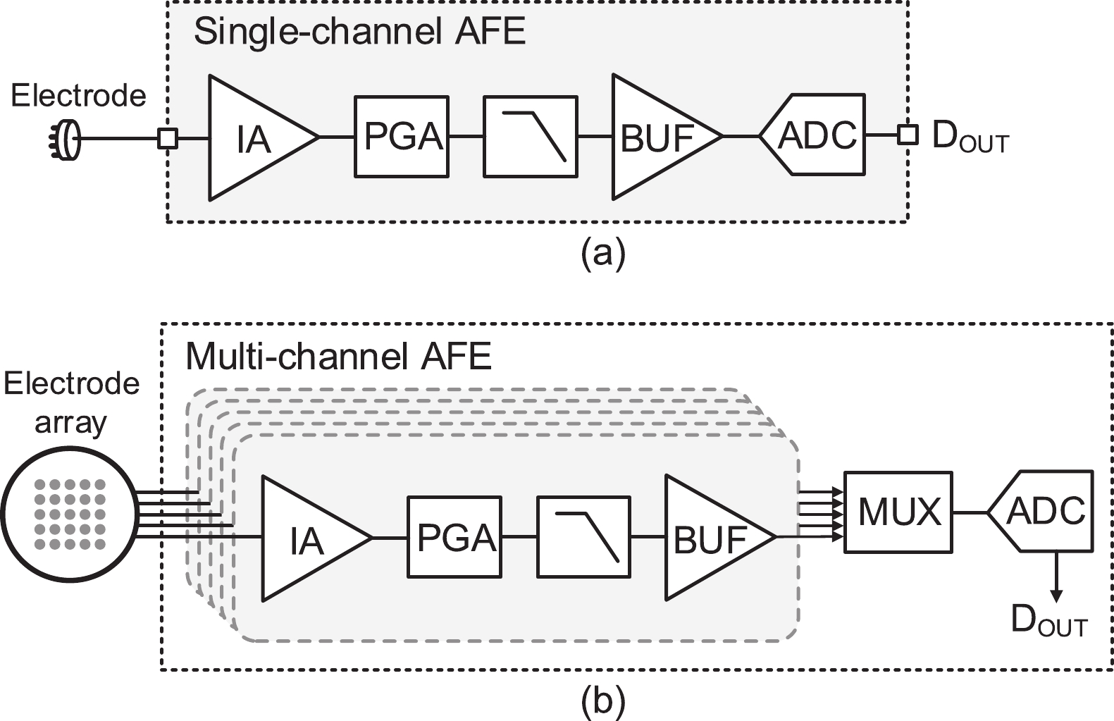
Fig. 1.
General bio-potential recording systems. (a) The single-channel AFE. (b) The multi-channel AFE.
ARTICLES
Yifan Huang, Jing Wang and Lin Cheng
Corresponding author: Jing Wang, jw2019@ustc.edu.cn
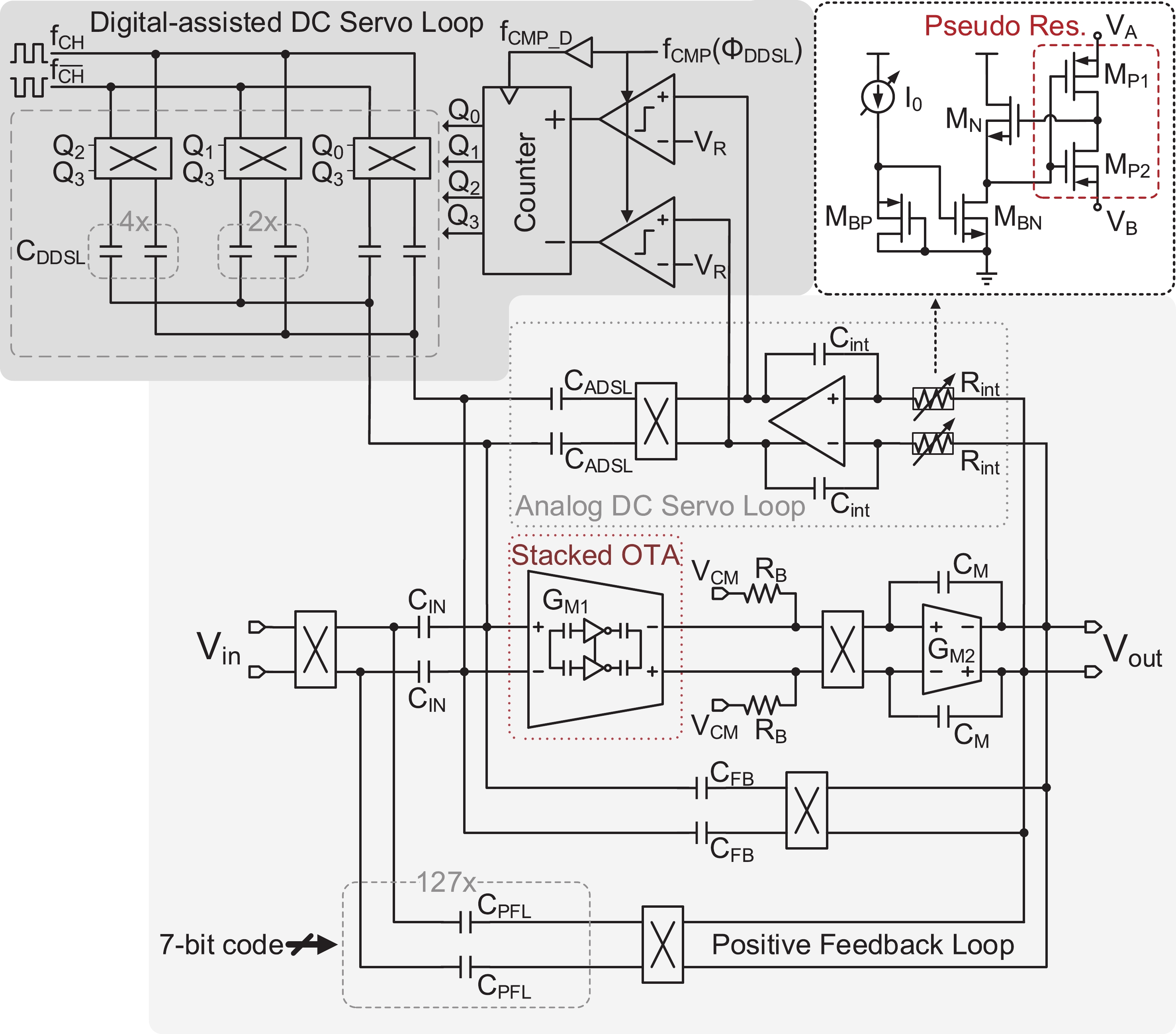
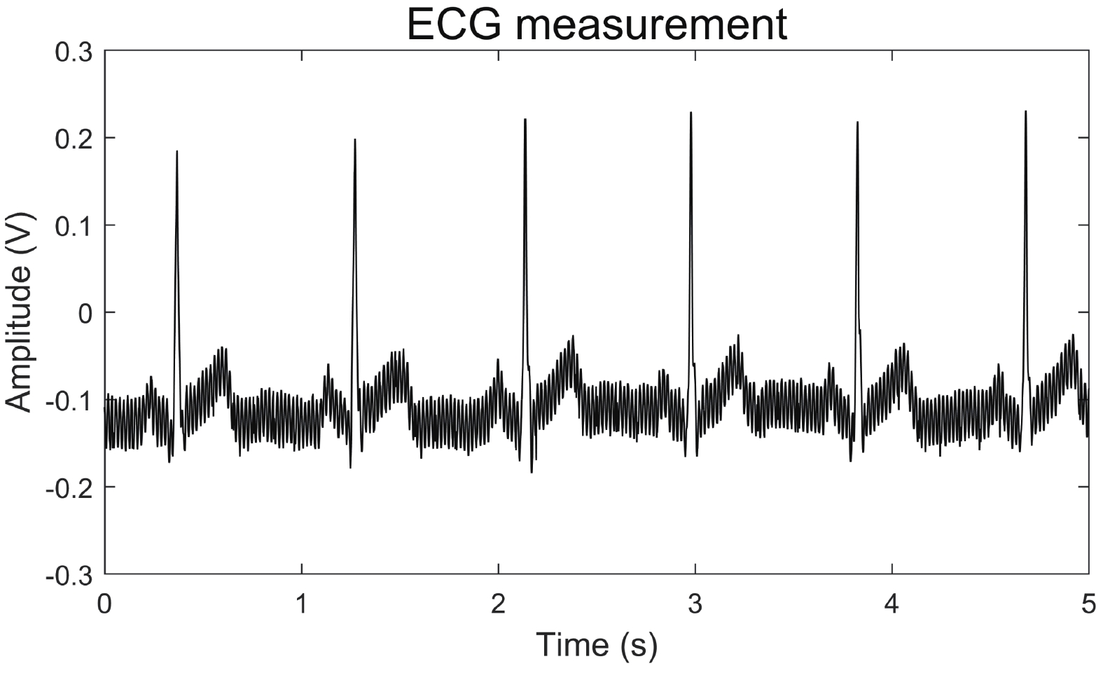
Abstract: This paper presents the design of a low-power multi-channel analog front-end (AFE) for bio-potential recording. By using time division multiplexing (TDM), a successive approximation register analog-to-digital converter (SAR ADC) is shared among all 20 channels. A charge-sharing multiplexer (MUX) is proposed to transmit the output signals from the respective channels to the ADC. By separately pre sampling the output of each channel, the sampling time of each channel is greatly extended and additional active buffers are avoided. The AFE is fabricated in a 65-nm CMOS process, and the whole system consumes 28.2 μW under 1 V supply. Each analog acquisition channel consumes 1.25 μW and occupies a chip area of 0.14 mm2. Measurement results show that the AFE achieves an input referred noise of 1.8 μV∙rms in a 350 Hz bandwidth and a noise efficiency factor (NEF) of 4.1. The 12-bit SAR ADC achieves an ENOB of 9.8 bit operating at 25 kS/s. The AFE is experimented on real-world applications by measuring human ECG and a clear ECG waveform is captured.
Key words: bio-potential recording, multi-channel, AFE, TDM, charge sharing, SAR ADC
| [1] |
Chae M, Liu W T, Yang Z, et al. A 128-channel 6mW wireless neural recording IC with on-the-fly spike sorting and UWB tansmitter. 2008 IEEE International Solid-State Circuits Conference-Digest of Technical Papers, 2008, 146 doi: 10.1109/ISSCC.2008.4523099
|
| [2] |
Zou X D, Liu L, Cheong J H, et al. A 100-channel 1-mW implantable neural recording IC. IEEE Trans Circuits Syst I Regul Pap, 2013, 60(10), 2584 doi: 10.1109/TCSI.2013.2249175
|
| [3] |
Li H Y, Shen Y T, Cantatore E, et al. A l0-bit 4 MS/s SAR ADC with fully-dynamic duty-cycled input driver. 2022 29th IEEE International Conference on Electronics, Circuits and Systems (ICECS), 2022, 1 doi: 10.1109/ICECS202256217.2022.9971059
|
| [4] |
Huang Y F, Liu J Y, Cheng L. A 1.7μW/channel time-division-multiplexing analog front-end for bio-potential recording. IEEE Trans Circuits Syst II Express Briefs, 2024, 71(8), 3640 doi: 10.1109/TCSII.2024.3367636
|
| [5] |
Craninckx J, van der Plas G. A 65fJ/conversion-step 0-to-50MS/s 0-to-0.7mW 9b charge-sharing SAR ADC in 90nm digital CMOS. 2007 IEEE International Solid-State Circuits Conference. Digest of Technical Papers, 2007, 246 doi: 10.1109/ISSCC.2007.373386
|
| [6] |
Giannini V, Nuzzo P, Chironi V, et al. An 820μW 9b 40MS/s noise-tolerant dynamic-SAR ADC in 90nm digital CMOS. 2008 IEEE International Solid-State Circuits Conference-Digest of Technical Papers, 2008, 238 doi: 10.1109/ISSCC.2008.4523145
|
| [7] |
Maddox M, Chen B Z, Coln M, et al. A 16 bit linear passive-charge-sharing SAR ADC in 55nm CMOS. 2016 IEEE Asian Solid-State Circuits Conference (A-SSCC), 2016, 153 doi: 10.1109/ASSCC.2016.7844158
|
| [8] |
Mondal S, Ghadami O, Hall D A. 10.2 A 139 µW 104.8dB-DR 24kHz-BW CT ΔΣM with chopped AC-coupled OTA-stacking and FIR DACs. 2021 IEEE International Solid- State Circuits Conference (ISSCC), 2021, 166 doi: 10.1109/ISSCC42613.2021.9366002
|
| [9] |
Zheng J W, Ki W H, Hu L Y, et al. Chopper capacitively coupled instrumentation amplifier capable of handling large electrode offset for biopotential recordings. IEEE Trans Circuits Syst II Express Briefs, 2017, 64(12), 1392 doi: 10.1109/TCSII.2017.2741348
|
| [10] |
Lee J, Lee K R, Ha U, et al. A 0.8-V 82.9-μW in-ear BCI controller IC with 8.8 PEF EEG instrumentation amplifier and wireless BAN transceiver. IEEE J Solid State Circuits, 2019, 54(4), 1185 doi: 10.1109/JSSC.2018.2888845
|
| [11] |
Djekic D, Ortmanns M, Fantner G, et al. A tunable, robust pseudo-resistor with enhanced linearity for scanning ion-conductance microscopy. 2016 IEEE International Symposium on Circuits and Systems (ISCAS), 2016, 842 doi: 10.1109/ISCAS.2016.7527372
|
| [12] |
Fan Q W, Sebastiano F, Huijsing J H, et al. A 1.8 μW 60 nV/√Hz capacitively-coupled chopper instrumentation amplifier in 65 nm CMOS for wireless sensor nodes. IEEE J Solid State Circuits, 2011, 46(7), 1534 doi: 10.1109/JSSC.2011.2143610
|
| [13] |
Liu C C, Chang S J, Huang G Y, et al. A 10-bit 50-MS/s SAR ADC with a monotonic capacitor switching procedure. IEEE J Solid State Circuits, 2010, 45(4), 731 doi: 10.1109/JSSC.2010.2042254
|
| [14] |
Harpe P, Cantatore E, van Roermund A. A 10b/12b 40 kS/s SAR ADC with data-driven noise reduction achieving up to 10.1b ENOB at 2.2 fJ/conversion-step. IEEE J Solid State Circuits, 2013, 48(12), 3011 doi: 10.1109/JSSC.2013.2278471
|
| [15] |
Steyaert M S J, Sansen W M C. A micropower low-noise monolithic instrumentation amplifier for medical purposes. IEEE J Solid State Circuits, 1987, 22(6), 1163 doi: 10.1109/JSSC.1987.1052869
|
| [16] |
Hsu Y P, Liu Z M, Hella M M. A 12.3-μW 0.72-mm² fully integrated front-end IC for arterial pulse waveform and ExG recording. IEEE J Solid State Circuits, 2020, 55(10), 2756 doi: 10.1109/JSSC.2020.3007177
|
| [17] |
Choi K J, Sim J Y. An 18.6-μW/Ch TDM-based 8-channel noncontact ECG recording IC with common-mode interference suppression. IEEE Trans Biomed Circuits Syst, 2022, 16(6), 1021 doi: 10.1109/TBCAS.2022.3229673
|
| [18] |
Rezaeiyan Y, Koolivand Y, Zamani M, et al. A 4.5μW miniaturized 3-channel wireless intra-cardiac acquisition system. IEEE Trans Biomed Circuits Syst, 2023, 17(5), 1097 doi: 10.1109/TBCAS.2023.3294560
|
| [19] |
Tian Y Y, Qin Z H, Yu Y, et al. A low-noise and low-power multi-channel ECG AFE based on orthogonal current-reuse amplifier. IEEE Trans Circuits Syst I Regul Pap, 2023, 70(8), 3167 doi: 10.1109/TCSI.2023.3277012
|
| [20] |
Zhang Y S, Yang C G, Sun J H, et al. A wireless headstage system based on neural-recording chip featuring 315 nW kickback-reduction SAR ADC. IEEE Trans Biomed Circuits Syst, 2023, 17(1), 105 doi: 10.1109/TBCAS.2022.3224387
|
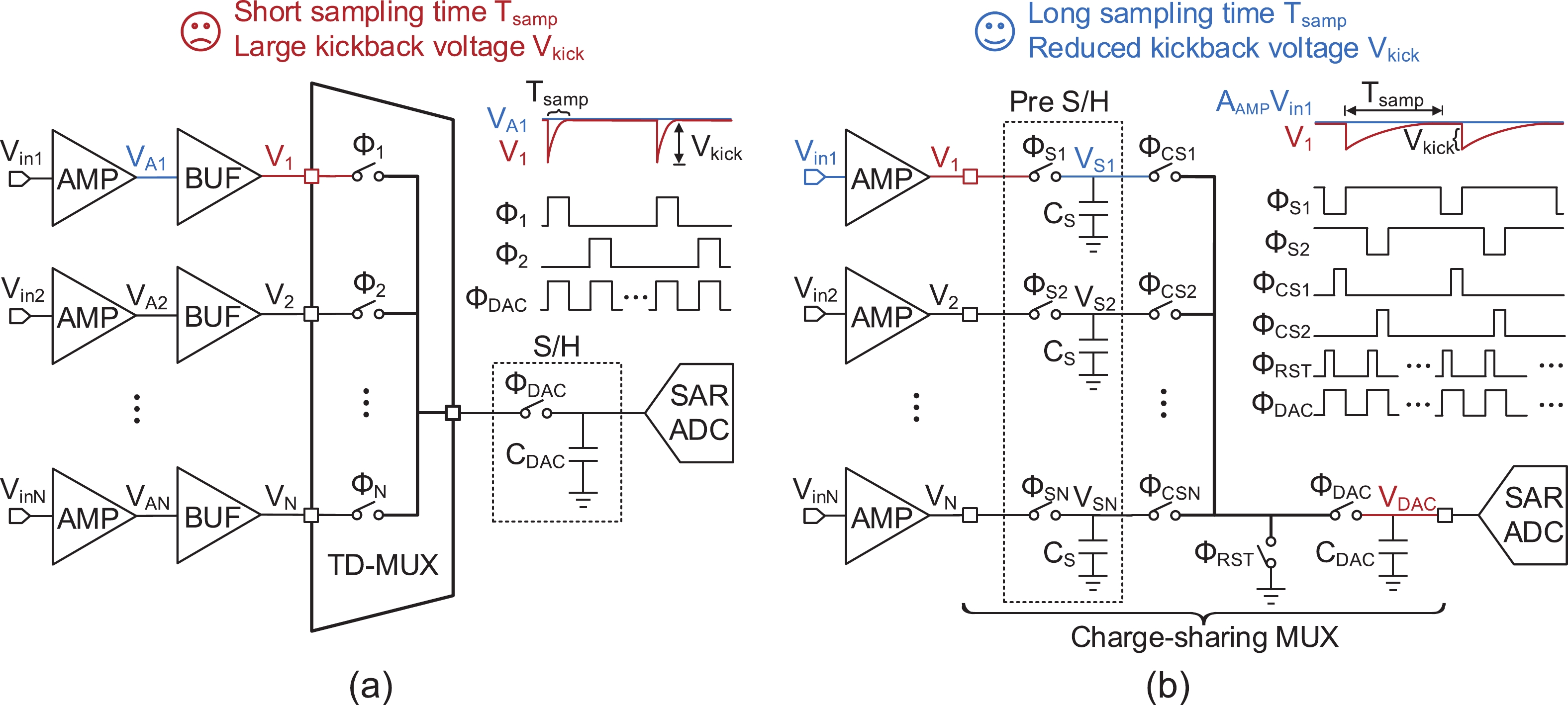
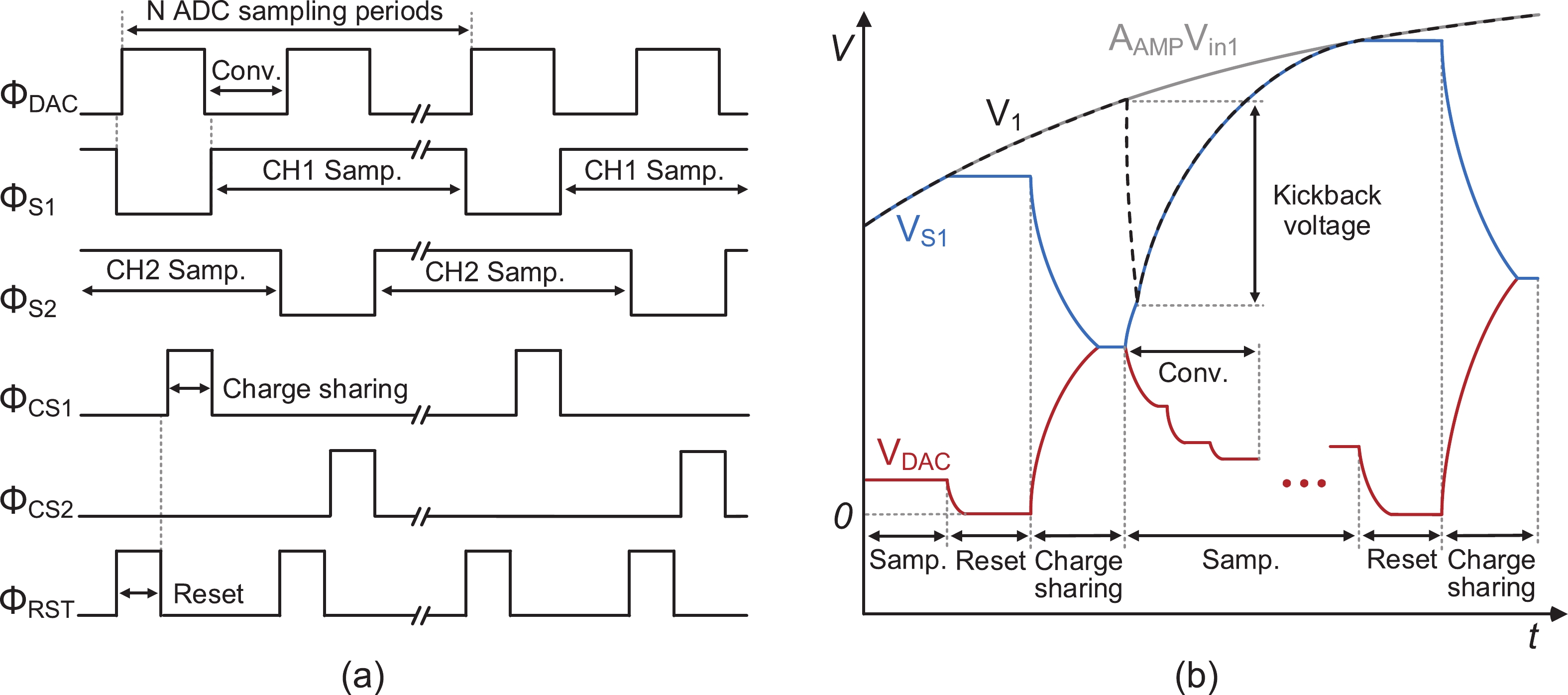
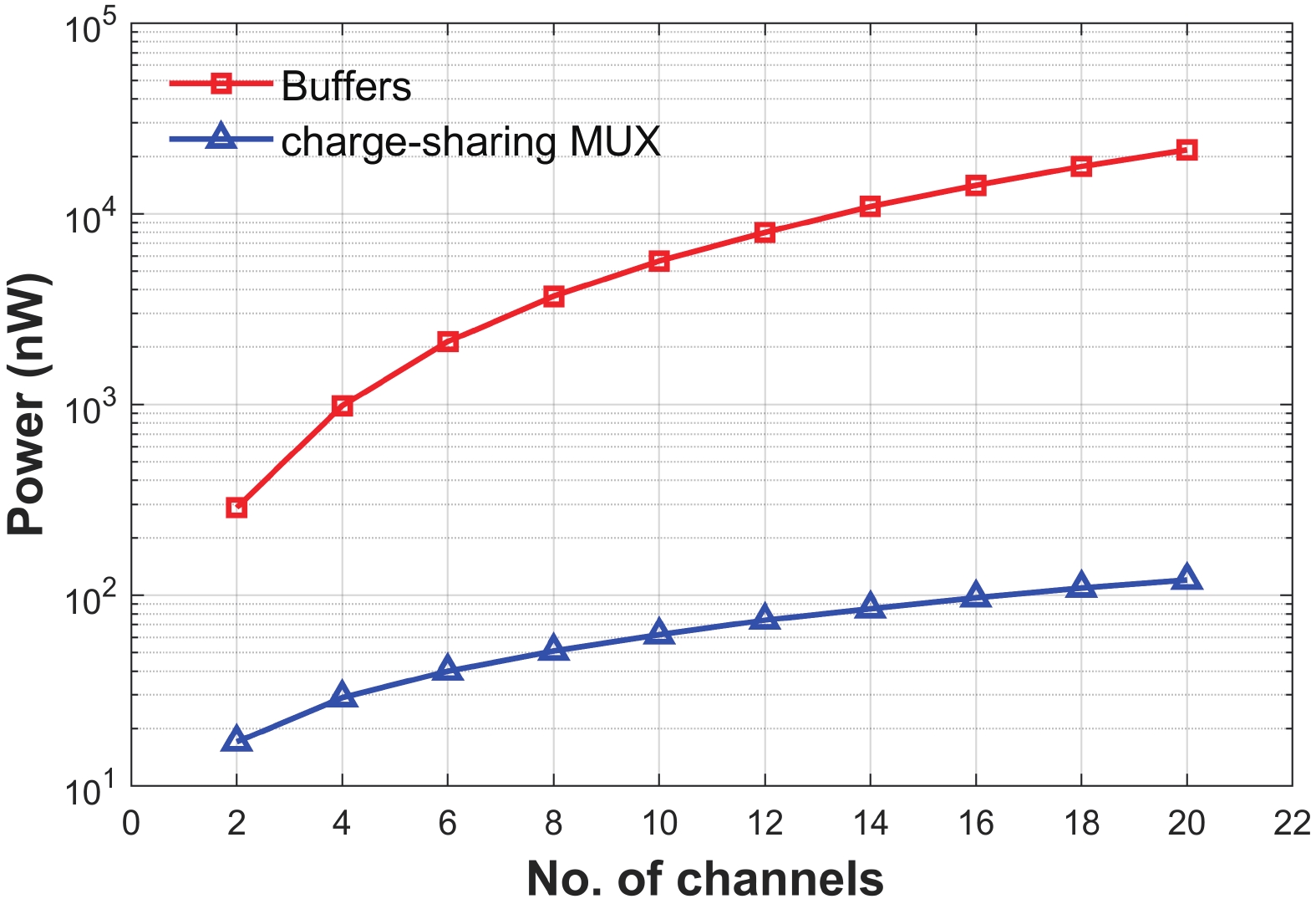
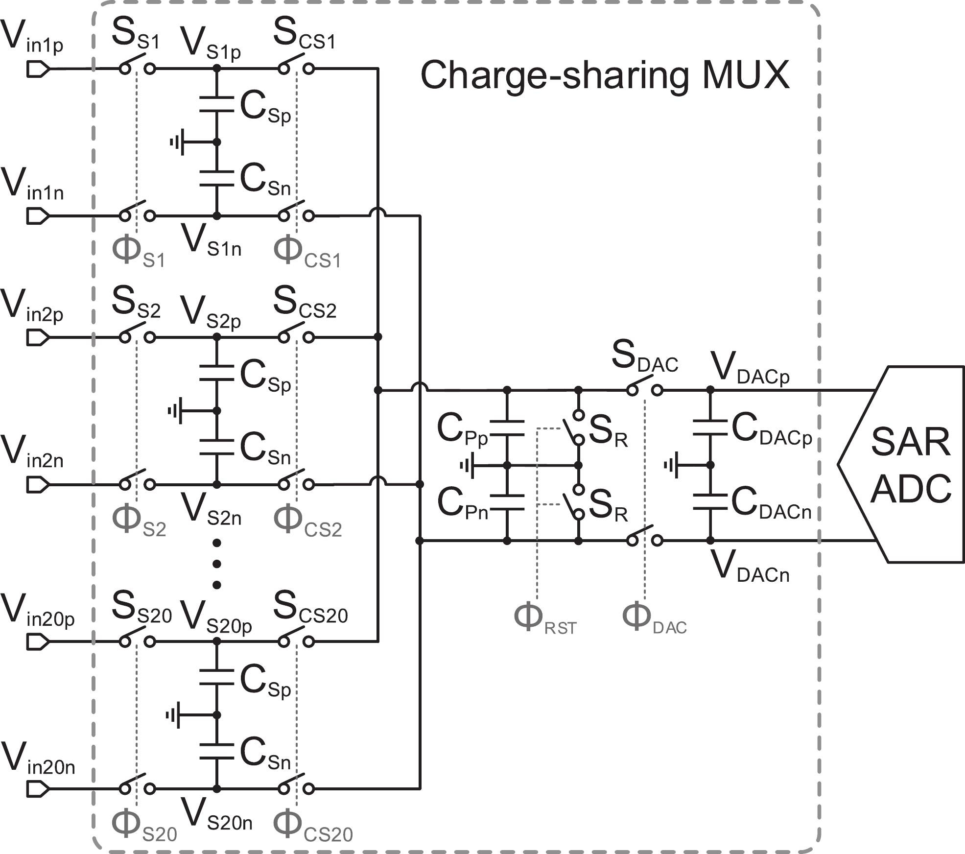
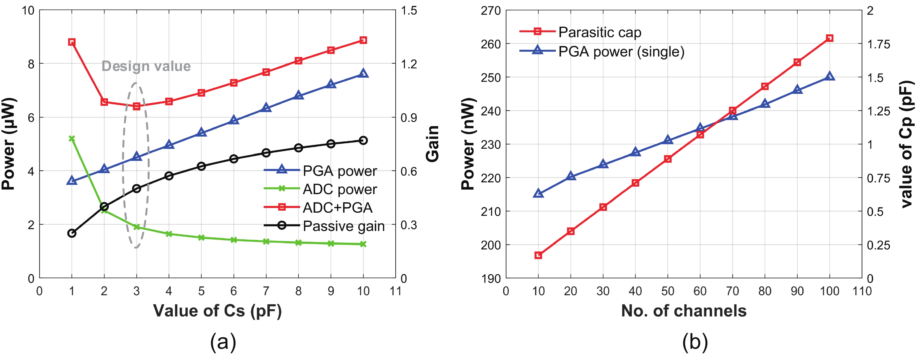
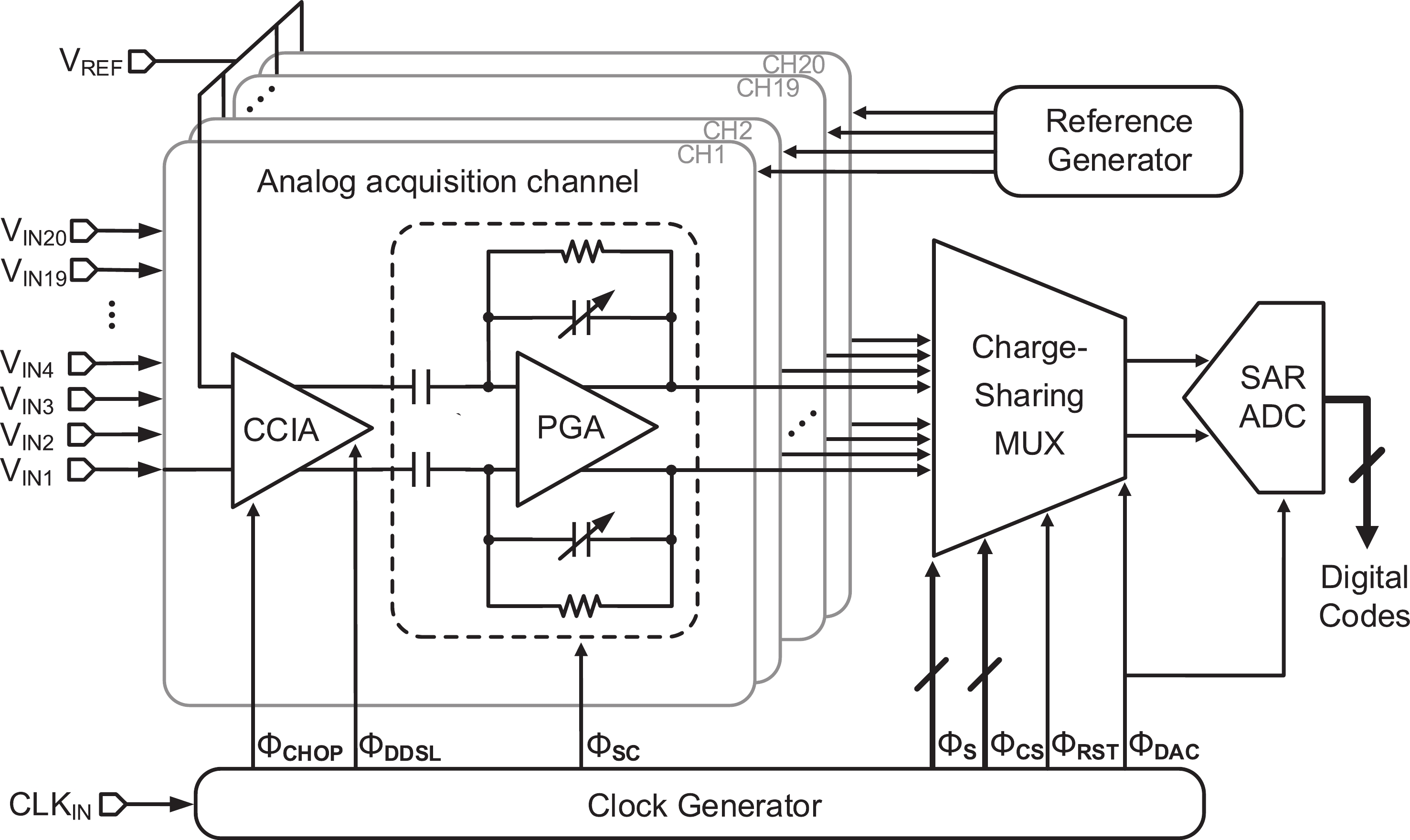
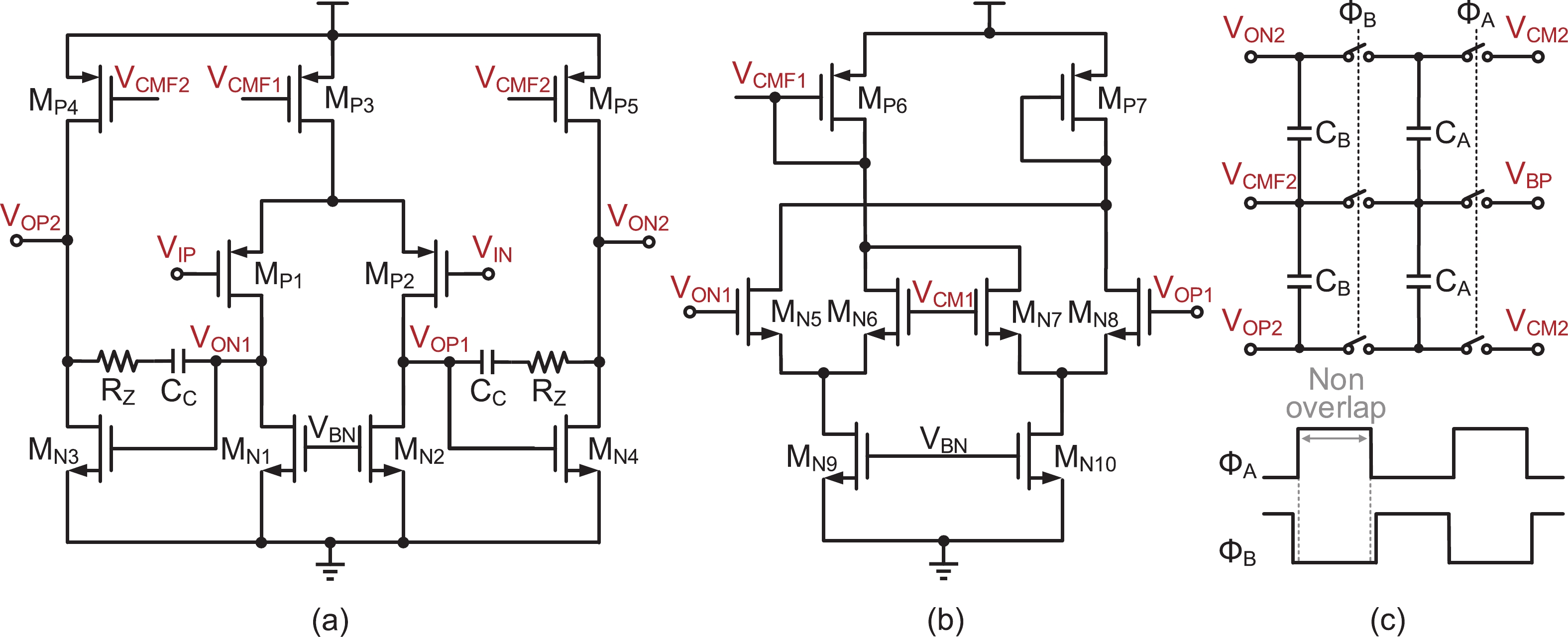

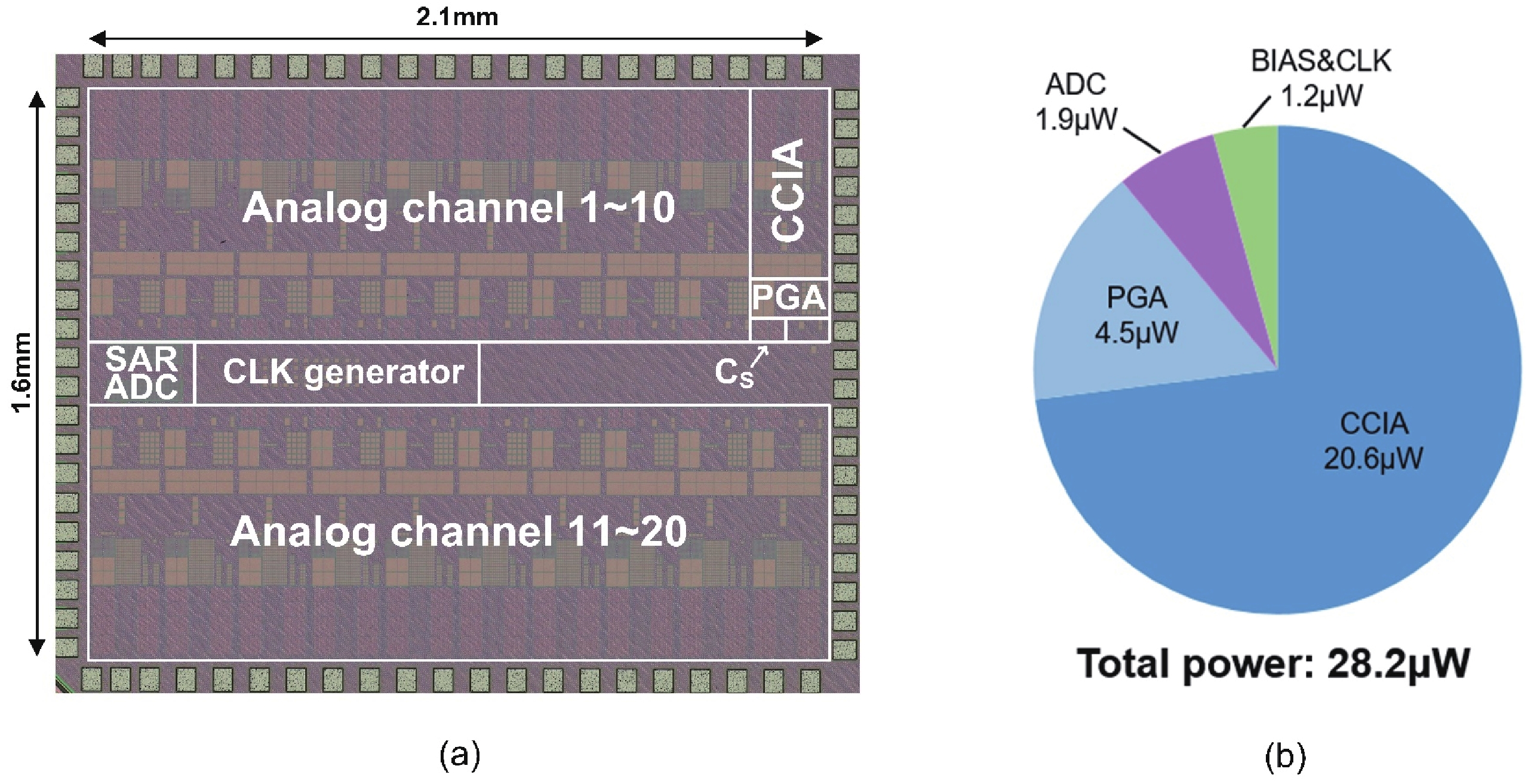
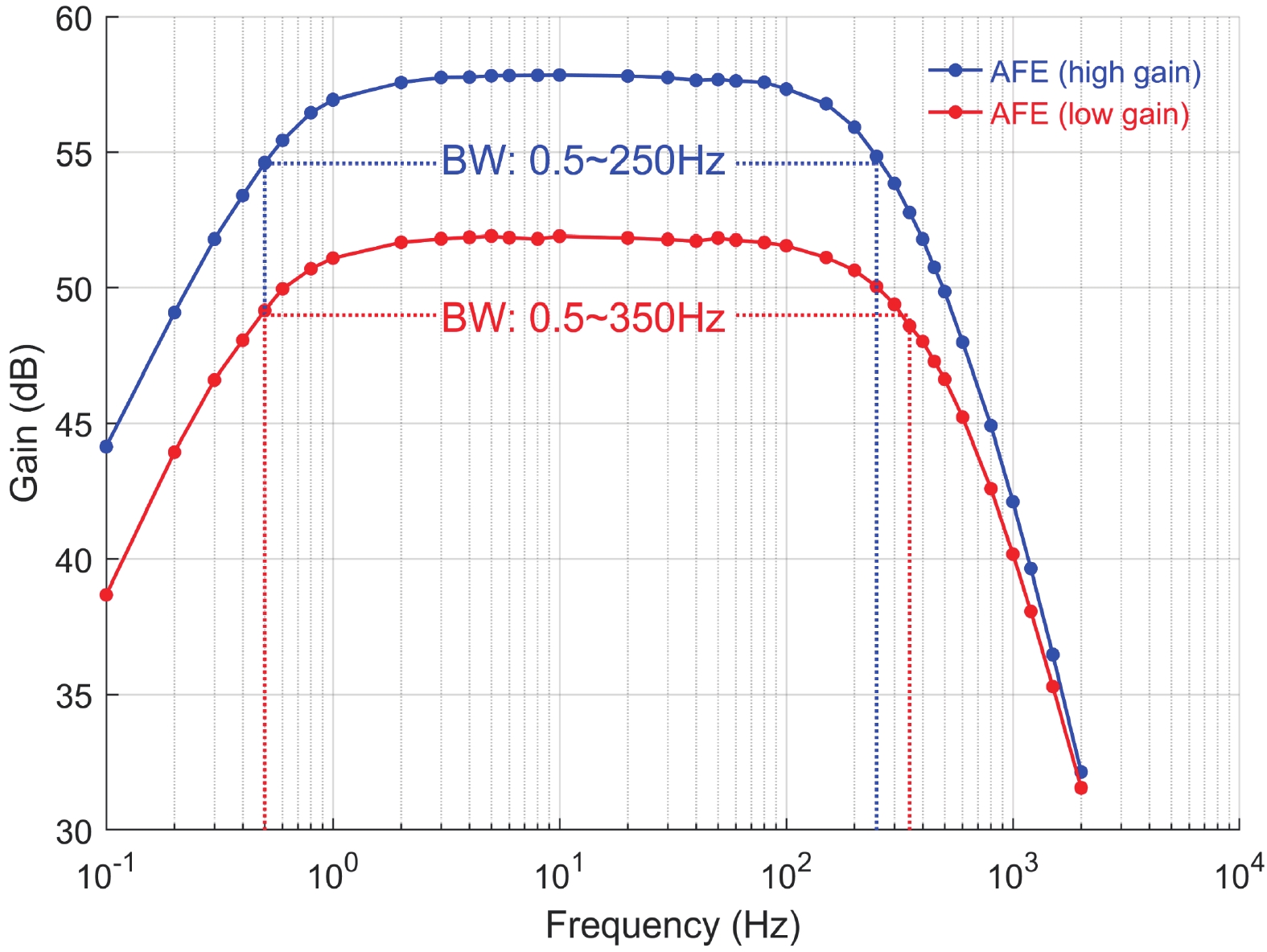
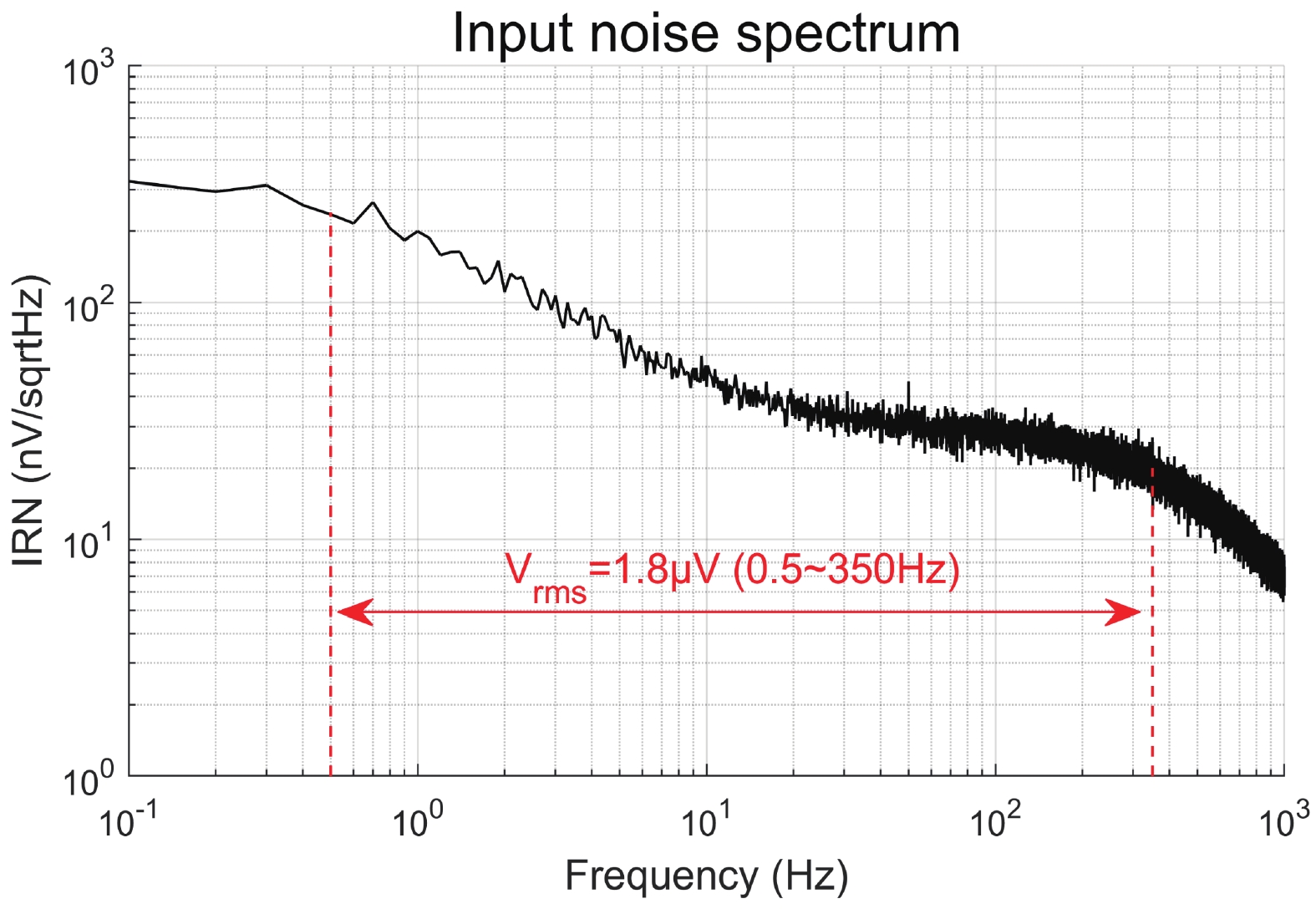
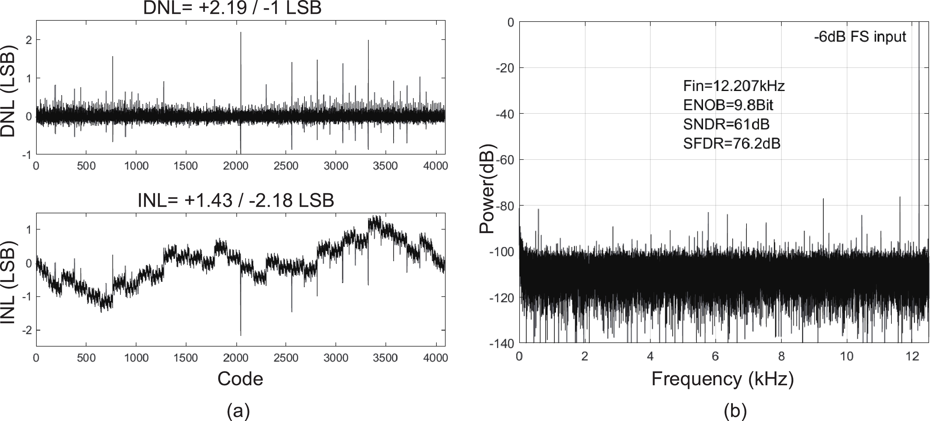
Table 1. Performance summary and comparison.
| Parameter | Ref. [16] | Ref. [17] | Ref. [18] | Ref. [19] | Ref. [20] | This work |
| Technology (nm) | 180 | 180 | 180 | 65 | 65 | 65 |
| Supply voltage (V) | 1.8 | 1.8 | 0.9 | 1.2 | 0.8 | 1 |
| Gain (dB) | 42−50 | 40.5 | 26−44 | 40.5−56 | 43.3 | 52/58 |
| Bandwidth (Hz) | 1k | 750 | 900 | 200/7k(IA) | 7.2k | 350/250 |
| IRN (μVrms) | 1.22 (1−100 Hz) |
0.84 (0.5−150 Hz) |
2.7 (0.15−200 Hz) |
2.68 (1−7 kHz) |
9.68 (0.9−7.2 kHz) |
1.8 (0.5−350 Hz) |
| NEF | 2.3 | 8.5 | 2.9(IA) | 1.81(IA) | 22.7 | 4.1 |
| CMRR (dB) | 100 | 102 | >75 | − | 83 | 84@50 Hz |
| Input impedance (MΩ) | − | 1830@50 Hz | − | >1000 | − | >300@50 Hz |
| Max EDO (mV) | − | ±600 | − | ±150 | Rail-to-rail | ±260 |
| ADC ENOB (bit) | 9.2 | 13.8 | 8.9 | − | 9.7 | 9.8 (0.5 FS) |
| # of channels | 1 | 8 | 3 | 4 | 8 | 20 |
| Power/ch (μW) | 5.3 | 18.6 | 1.5 | 2.6 | 18.4 | 1.25 |
| Area/ch (mm2) | 0.72 | 0.176 | 1.125 | 0.24 | 0.113 | 0.14 |
 DownLoad: CSV
| [1] |
Chae M, Liu W T, Yang Z, et al. A 128-channel 6mW wireless neural recording IC with on-the-fly spike sorting and UWB tansmitter. 2008 IEEE International Solid-State Circuits Conference-Digest of Technical Papers, 2008, 146 doi: 10.1109/ISSCC.2008.4523099
|
| [2] |
Zou X D, Liu L, Cheong J H, et al. A 100-channel 1-mW implantable neural recording IC. IEEE Trans Circuits Syst I Regul Pap, 2013, 60(10), 2584 doi: 10.1109/TCSI.2013.2249175
|
| [3] |
Li H Y, Shen Y T, Cantatore E, et al. A l0-bit 4 MS/s SAR ADC with fully-dynamic duty-cycled input driver. 2022 29th IEEE International Conference on Electronics, Circuits and Systems (ICECS), 2022, 1 doi: 10.1109/ICECS202256217.2022.9971059
|
| [4] |
Huang Y F, Liu J Y, Cheng L. A 1.7μW/channel time-division-multiplexing analog front-end for bio-potential recording. IEEE Trans Circuits Syst II Express Briefs, 2024, 71(8), 3640 doi: 10.1109/TCSII.2024.3367636
|
| [5] |
Craninckx J, van der Plas G. A 65fJ/conversion-step 0-to-50MS/s 0-to-0.7mW 9b charge-sharing SAR ADC in 90nm digital CMOS. 2007 IEEE International Solid-State Circuits Conference. Digest of Technical Papers, 2007, 246 doi: 10.1109/ISSCC.2007.373386
|
| [6] |
Giannini V, Nuzzo P, Chironi V, et al. An 820μW 9b 40MS/s noise-tolerant dynamic-SAR ADC in 90nm digital CMOS. 2008 IEEE International Solid-State Circuits Conference-Digest of Technical Papers, 2008, 238 doi: 10.1109/ISSCC.2008.4523145
|
| [7] |
Maddox M, Chen B Z, Coln M, et al. A 16 bit linear passive-charge-sharing SAR ADC in 55nm CMOS. 2016 IEEE Asian Solid-State Circuits Conference (A-SSCC), 2016, 153 doi: 10.1109/ASSCC.2016.7844158
|
| [8] |
Mondal S, Ghadami O, Hall D A. 10.2 A 139 µW 104.8dB-DR 24kHz-BW CT ΔΣM with chopped AC-coupled OTA-stacking and FIR DACs. 2021 IEEE International Solid- State Circuits Conference (ISSCC), 2021, 166 doi: 10.1109/ISSCC42613.2021.9366002
|
| [9] |
Zheng J W, Ki W H, Hu L Y, et al. Chopper capacitively coupled instrumentation amplifier capable of handling large electrode offset for biopotential recordings. IEEE Trans Circuits Syst II Express Briefs, 2017, 64(12), 1392 doi: 10.1109/TCSII.2017.2741348
|
| [10] |
Lee J, Lee K R, Ha U, et al. A 0.8-V 82.9-μW in-ear BCI controller IC with 8.8 PEF EEG instrumentation amplifier and wireless BAN transceiver. IEEE J Solid State Circuits, 2019, 54(4), 1185 doi: 10.1109/JSSC.2018.2888845
|
| [11] |
Djekic D, Ortmanns M, Fantner G, et al. A tunable, robust pseudo-resistor with enhanced linearity for scanning ion-conductance microscopy. 2016 IEEE International Symposium on Circuits and Systems (ISCAS), 2016, 842 doi: 10.1109/ISCAS.2016.7527372
|
| [12] |
Fan Q W, Sebastiano F, Huijsing J H, et al. A 1.8 μW 60 nV/√Hz capacitively-coupled chopper instrumentation amplifier in 65 nm CMOS for wireless sensor nodes. IEEE J Solid State Circuits, 2011, 46(7), 1534 doi: 10.1109/JSSC.2011.2143610
|
| [13] |
Liu C C, Chang S J, Huang G Y, et al. A 10-bit 50-MS/s SAR ADC with a monotonic capacitor switching procedure. IEEE J Solid State Circuits, 2010, 45(4), 731 doi: 10.1109/JSSC.2010.2042254
|
| [14] |
Harpe P, Cantatore E, van Roermund A. A 10b/12b 40 kS/s SAR ADC with data-driven noise reduction achieving up to 10.1b ENOB at 2.2 fJ/conversion-step. IEEE J Solid State Circuits, 2013, 48(12), 3011 doi: 10.1109/JSSC.2013.2278471
|
| [15] |
Steyaert M S J, Sansen W M C. A micropower low-noise monolithic instrumentation amplifier for medical purposes. IEEE J Solid State Circuits, 1987, 22(6), 1163 doi: 10.1109/JSSC.1987.1052869
|
| [16] |
Hsu Y P, Liu Z M, Hella M M. A 12.3-μW 0.72-mm² fully integrated front-end IC for arterial pulse waveform and ExG recording. IEEE J Solid State Circuits, 2020, 55(10), 2756 doi: 10.1109/JSSC.2020.3007177
|
| [17] |
Choi K J, Sim J Y. An 18.6-μW/Ch TDM-based 8-channel noncontact ECG recording IC with common-mode interference suppression. IEEE Trans Biomed Circuits Syst, 2022, 16(6), 1021 doi: 10.1109/TBCAS.2022.3229673
|
| [18] |
Rezaeiyan Y, Koolivand Y, Zamani M, et al. A 4.5μW miniaturized 3-channel wireless intra-cardiac acquisition system. IEEE Trans Biomed Circuits Syst, 2023, 17(5), 1097 doi: 10.1109/TBCAS.2023.3294560
|
| [19] |
Tian Y Y, Qin Z H, Yu Y, et al. A low-noise and low-power multi-channel ECG AFE based on orthogonal current-reuse amplifier. IEEE Trans Circuits Syst I Regul Pap, 2023, 70(8), 3167 doi: 10.1109/TCSI.2023.3277012
|
| [20] |
Zhang Y S, Yang C G, Sun J H, et al. A wireless headstage system based on neural-recording chip featuring 315 nW kickback-reduction SAR ADC. IEEE Trans Biomed Circuits Syst, 2023, 17(1), 105 doi: 10.1109/TBCAS.2022.3224387
|


Article views: 200 Times PDF downloads: 43 Times Cited by: 0 Times
Received: 05 December 2024 Revised: 08 March 2025 Online: Accepted Manuscript: 30 April 2025Uncorrected proof: 19 May 2025
| Citation: |
Yifan Huang, Jing Wang, Lin Cheng. A 1.25 μW/ch TDM-based analog front-end using a charge-sharing multiplexer for bio-potential recording[J]. Journal of Semiconductors, 2025, In Press. doi: 10.1088/1674-4926/24120034
****
Y F Huang, J Wang, and L Cheng, A 1.25 μW/ch TDM-based analog front-end using a charge-sharing multiplexer for bio-potential recording[J]. J. Semicond., 2025, 46(10), 102203 doi: 10.1088/1674-4926/24120034

|
 Yifan Huang received the B.Eng. degree in Electronic Science and Technology from University of Science and Technology of China, Hefei, China, in 2018. He is currently pursuing the D.Eng. degree with the School of Microelectronics, University of Science and Technology of China, Hefei, China. His research interests include the design of mixed-signal and low-power integrated circuits for biomedical applications
 Jing Wang received the B.Eng. degree from Sichuan University, Chengdu, China, in 2011. Then, she received the M. Sc. degree in 2012 and the Ph.D. degree in 2017 from Waseda University, Fukuoka, Japan, respectively. From 2017 to 2019, she was a post doctor in Waseda University, Japan. She is currently an associate researcher at the University of Science and Technology of China. Her research focuses on the design of high-precision, low-power analog front-end (AFE) circuits
 Lin Cheng received the B.Eng. degree from Hefei University of Technology, Hefei, China, in 2008, the M. Sc. degree from Fudan University, Shanghai, China, in 2011, and the Ph.D. degree from Hong Kong University of Science and Technology (HKUST), Hong Kong, in 2016. In 2018, he joined the School of Microelectronics, University of Science and Technology of China, Hefei, where he is currently a Professor. He was a Post-doctoral Research Associate at the Department of Electronic and Computer Engineering, HKUST, from 2016 to 2018, and was an Intern Analog Design Engineer with Broadcom Limited, San Jose, CA, USA, from 2015 to 2016. His current research interests include power management and mixed-signal integrated circuits and systems, wireless power transfer circuits and systems, switched-inductor power converters, and automotive ICs. Dr. Cheng is serving as a member of the ISSCC Technical Committee and the Chair of the IEEE ICTA 2024 Technical Committee. He was a recipient of the IEEE Solid-State Circuits Society Pre-Doctoral Achievement Award from 2014 to 2015, the Hong Kong Institution of Science 2018 Young Scientist Awards (Honorable Mention), and the Best Design Award from the IEEE ASP-DAC University Design Contest in 2020
| [1] |
Chae M, Liu W T, Yang Z, et al. A 128-channel 6mW wireless neural recording IC with on-the-fly spike sorting and UWB tansmitter. 2008 IEEE International Solid-State Circuits Conference-Digest of Technical Papers, 2008, 146 doi: 10.1109/ISSCC.2008.4523099
|
| [2] |
Zou X D, Liu L, Cheong J H, et al. A 100-channel 1-mW implantable neural recording IC. IEEE Trans Circuits Syst I Regul Pap, 2013, 60(10), 2584 doi: 10.1109/TCSI.2013.2249175
|
| [3] |
Li H Y, Shen Y T, Cantatore E, et al. A l0-bit 4 MS/s SAR ADC with fully-dynamic duty-cycled input driver. 2022 29th IEEE International Conference on Electronics, Circuits and Systems (ICECS), 2022, 1 doi: 10.1109/ICECS202256217.2022.9971059
|
| [4] |
Huang Y F, Liu J Y, Cheng L. A 1.7μW/channel time-division-multiplexing analog front-end for bio-potential recording. IEEE Trans Circuits Syst II Express Briefs, 2024, 71(8), 3640 doi: 10.1109/TCSII.2024.3367636
|
| [5] |
Craninckx J, van der Plas G. A 65fJ/conversion-step 0-to-50MS/s 0-to-0.7mW 9b charge-sharing SAR ADC in 90nm digital CMOS. 2007 IEEE International Solid-State Circuits Conference. Digest of Technical Papers, 2007, 246 doi: 10.1109/ISSCC.2007.373386
|
| [6] |
Giannini V, Nuzzo P, Chironi V, et al. An 820μW 9b 40MS/s noise-tolerant dynamic-SAR ADC in 90nm digital CMOS. 2008 IEEE International Solid-State Circuits Conference-Digest of Technical Papers, 2008, 238 doi: 10.1109/ISSCC.2008.4523145
|
| [7] |
Maddox M, Chen B Z, Coln M, et al. A 16 bit linear passive-charge-sharing SAR ADC in 55nm CMOS. 2016 IEEE Asian Solid-State Circuits Conference (A-SSCC), 2016, 153 doi: 10.1109/ASSCC.2016.7844158
|
| [8] |
Mondal S, Ghadami O, Hall D A. 10.2 A 139 µW 104.8dB-DR 24kHz-BW CT ΔΣM with chopped AC-coupled OTA-stacking and FIR DACs. 2021 IEEE International Solid- State Circuits Conference (ISSCC), 2021, 166 doi: 10.1109/ISSCC42613.2021.9366002
|
| [9] |
Zheng J W, Ki W H, Hu L Y, et al. Chopper capacitively coupled instrumentation amplifier capable of handling large electrode offset for biopotential recordings. IEEE Trans Circuits Syst II Express Briefs, 2017, 64(12), 1392 doi: 10.1109/TCSII.2017.2741348
|
| [10] |
Lee J, Lee K R, Ha U, et al. A 0.8-V 82.9-μW in-ear BCI controller IC with 8.8 PEF EEG instrumentation amplifier and wireless BAN transceiver. IEEE J Solid State Circuits, 2019, 54(4), 1185 doi: 10.1109/JSSC.2018.2888845
|
| [11] |
Djekic D, Ortmanns M, Fantner G, et al. A tunable, robust pseudo-resistor with enhanced linearity for scanning ion-conductance microscopy. 2016 IEEE International Symposium on Circuits and Systems (ISCAS), 2016, 842 doi: 10.1109/ISCAS.2016.7527372
|
| [12] |
Fan Q W, Sebastiano F, Huijsing J H, et al. A 1.8 μW 60 nV/√Hz capacitively-coupled chopper instrumentation amplifier in 65 nm CMOS for wireless sensor nodes. IEEE J Solid State Circuits, 2011, 46(7), 1534 doi: 10.1109/JSSC.2011.2143610
|
| [13] |
Liu C C, Chang S J, Huang G Y, et al. A 10-bit 50-MS/s SAR ADC with a monotonic capacitor switching procedure. IEEE J Solid State Circuits, 2010, 45(4), 731 doi: 10.1109/JSSC.2010.2042254
|
| [14] |
Harpe P, Cantatore E, van Roermund A. A 10b/12b 40 kS/s SAR ADC with data-driven noise reduction achieving up to 10.1b ENOB at 2.2 fJ/conversion-step. IEEE J Solid State Circuits, 2013, 48(12), 3011 doi: 10.1109/JSSC.2013.2278471
|
| [15] |
Steyaert M S J, Sansen W M C. A micropower low-noise monolithic instrumentation amplifier for medical purposes. IEEE J Solid State Circuits, 1987, 22(6), 1163 doi: 10.1109/JSSC.1987.1052869
|
| [16] |
Hsu Y P, Liu Z M, Hella M M. A 12.3-μW 0.72-mm² fully integrated front-end IC for arterial pulse waveform and ExG recording. IEEE J Solid State Circuits, 2020, 55(10), 2756 doi: 10.1109/JSSC.2020.3007177
|
| [17] |
Choi K J, Sim J Y. An 18.6-μW/Ch TDM-based 8-channel noncontact ECG recording IC with common-mode interference suppression. IEEE Trans Biomed Circuits Syst, 2022, 16(6), 1021 doi: 10.1109/TBCAS.2022.3229673
|
| [18] |
Rezaeiyan Y, Koolivand Y, Zamani M, et al. A 4.5μW miniaturized 3-channel wireless intra-cardiac acquisition system. IEEE Trans Biomed Circuits Syst, 2023, 17(5), 1097 doi: 10.1109/TBCAS.2023.3294560
|
| [19] |
Tian Y Y, Qin Z H, Yu Y, et al. A low-noise and low-power multi-channel ECG AFE based on orthogonal current-reuse amplifier. IEEE Trans Circuits Syst I Regul Pap, 2023, 70(8), 3167 doi: 10.1109/TCSI.2023.3277012
|
| [20] |
Zhang Y S, Yang C G, Sun J H, et al. A wireless headstage system based on neural-recording chip featuring 315 nW kickback-reduction SAR ADC. IEEE Trans Biomed Circuits Syst, 2023, 17(1), 105 doi: 10.1109/TBCAS.2022.3224387
|

 WeChat ID
Journal of Semiconductors © 2017 All Rights Reserved 京ICP备05085259号-2