


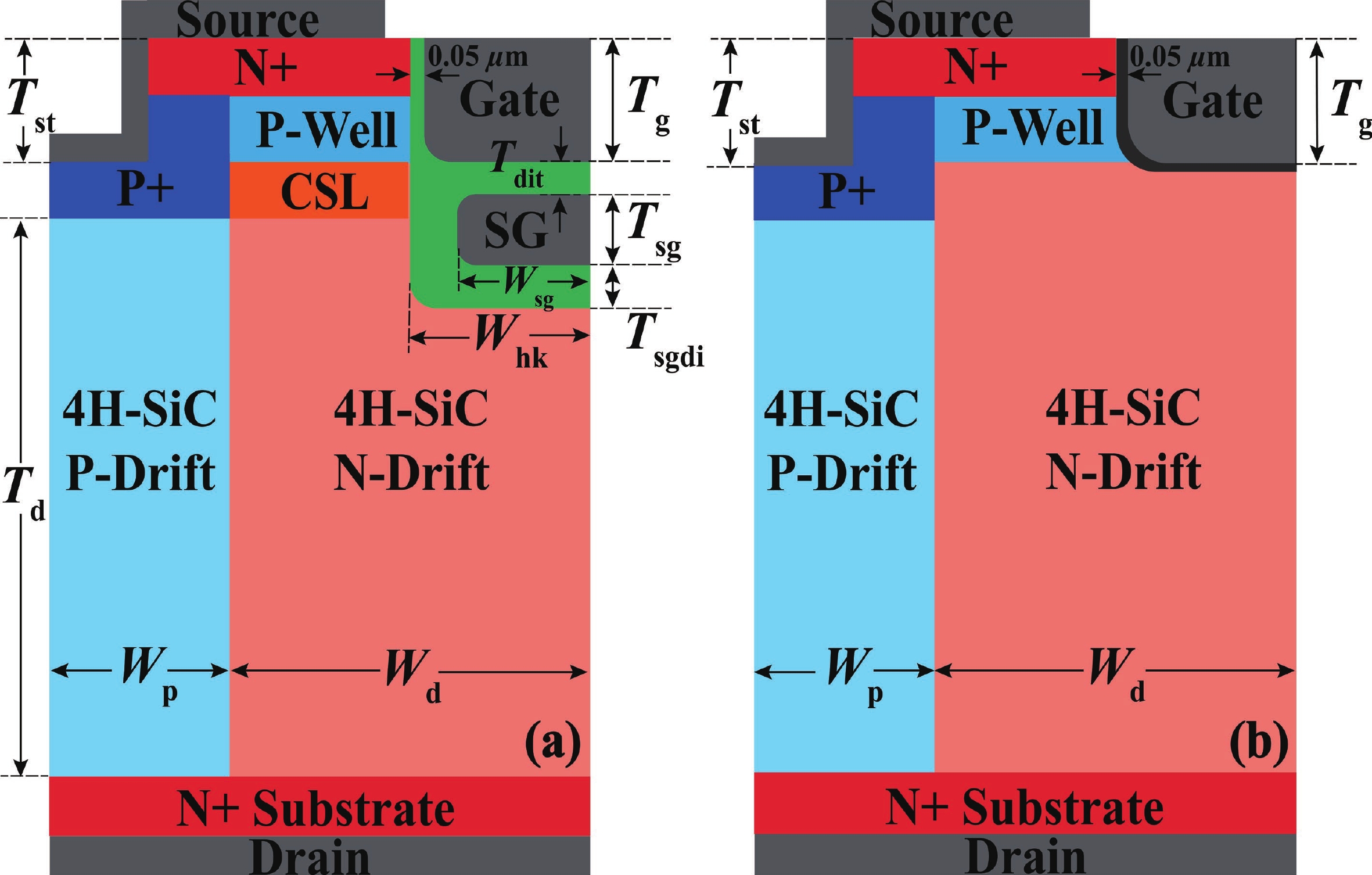
Fig. 1.
(Color online) Schematic of the proposed (a) HKSG-SJMOS and (b) CONV-SJMOS.
ARTICLES
Jiafei Yao1, 2, 3, Zhengfei Yang1, 2, 3, Yuxuan Dai1, 2, 3, Ziwei Hu1, 2, 3, Man Li1, 2, Kemeng Yang1, 2, Jing Chen1, 2, Maolin Zhang1, 2, Jun Zhang1, 2 and Yufeng Guo1, 2,
Corresponding author: Yufeng Guo, yfguo@njupt.edu.cn
Abstract: A 4H-SiC superjunction (SJ) MOSFET (SJMOS) with integrated high-K gate dielectric and split gate (HKSG-SJMOS) is proposed in this paper. The key features of HKSG-SJMOS involve the utilization of high-K (HK) dielectric as the gate dielectric, which surrounds the source-connected split gate (SG) and metal gate. The high-K gate dielectric optimizes the electric field distribution within the drift region, creating a low-resistance conductive channel. This enhancement leads to an increase in the breakdown voltage (BV) and a reduction in the specific on resistance (Ron,sp). The introduction of split gate surrounded by high-K dielectric reduces the gate−drain capacitance (Cgd) and gate−drain charge (Qgd), which improves the switching characteristics. The simulation results indicate that compared to conventional 4H-SiC SJMOS, the HKSG-SJMOS exhibits a 110.5% enhancement in figure of merit (FOM, FOM = BV2/Ron,sp), a 93.6% reduction in the high frequency figure of merit (HFFOM) of Ron,sp·Cgd, and reductions in turn-on loss (Eon) and turn-off loss (Eoff) by 38.3% and 31.6%, respectively. Furthermore, the reverse recovery characteristics of HKSG-SJMOS has also discussed, revealing superior performance compared to conventional 4H-SiC SJMOS.
Key words: split gate, superjunction, high-K dielectric, 4H-SiC, MOSFET
| [1] |
Nan Y G, Han G Q. 4H–SiC floating junction Schottky barrier diode with compensation layer of engineered cathode structure: Cone–shaped electric field, current density waveform, and applications. Microelectron J, 2022, 125, 105472 doi: 10.1016/j.mejo.2022.105472
|
| [2] |
Luo M J, Zhang Y R, Wang Y C, et al. Design and modelling of SiC MPS diodes with superior surge current robustness. Microelectron J, 2024, 151, 106298 doi: 10.1016/j.mejo.2024.106298
|
| [3] |
Luo M J, Chen H, Zhang Y R, et al. Novel design and modelling of SiC junction barrier Schottky diode with improved Baliga FOM under high–temperature applications. Microelectron J, 2024, 151, 106343 doi: 10.1016/j.mejo.2024.106343
|
| [4] |
Wu L J, Yang G L, Yang D Q, et al. Self–clamped P–shield 4H–SiC trench MOSFET for low turn–off loss and suppress switching oscillation. Microelectron J, 2024, 151, 106307 doi: 10.1016/j.mejo.2024.106307
|
| [5] |
Harada S, Kobayashi Y, Kyogoku S, et al. First demonstration of dynamic characteristics for SiC superjunction MOSFET realized using multi–epitaxial growth method. 2018 IEEE International Electron Devices Meeting (IEDM), 2018, 8.2.1 doi: 10.1109/IEDM.2018.8614670
|
| [6] |
Kosugi R, Ji S Y, Mochizuki K, et al. Breaking the theoretical limit of 6.5 kV–class 4H–SiC super–junction (SJ) MOSFETs by trench–filling epitaxial growth. 2019 31st International Symposium on Power Semiconductor Devices and ICs (ISPSD), 2019, 39 doi: 10.1109/ISPSD.2019.8757632
|
| [7] |
Okada M, Kyogoku S, Kumazawa T, et al. Superior short–circuit performance of SiC superjunction MOSFET. 2020 32nd International Symposium on Power Semiconductor Devices and ICs (ISPSD), 2020, 70 doi: 10.1109/ISPSD46842.2020.9170126
|
| [8] |
Wang X J, Shen Z W, Zhang G L, et al. A 4H–SiC semi–super–junction shielded trench MOSFET: P–pillar is grounded to optimize the electric field characteristics. J Semicond, 2022, 43(12), 85 doi: 10.1088/1674-4926/43/12/122802
|
| [9] |
Ding J Y, Wei W S. An UMOSFET integrated with graded semi–super–junction and 3C/4H–SiC hetero–crystalline freewheeling junction. Microelectron J, 2023, 142, 105992 doi: 10.1016/j.mejo.2023.105992
|
| [10] |
Kim J, Kim K. A novel 4H–SiC super junction UMOSFET with heterojunction diode for enhanced reverse recovery characteristics. 2020 International Conference on Electronics, Information, and Communication (ICEIC) , 2020, 1 doi: 10.1109/ICEIC49074.2020.9051221
|
| [11] |
Yao J F, Yang Z F, Zhu Y Q, et al. Performance enhancement of 4H–SiC superjunction trench MOSFET with extended high–K dielectric. Microelectron J, 2024, 151, 106359 doi: 10.1016/j.mejo.2024.106359
|
| [12] |
Yao J F, Liu Y A, Li A, et al. Investigations of 4H–SiC trench MOSFET with integrated high–K deep trench and gate dielectric. IET Power Electron, 2024, 17(7), 869 doi: 10.1049/pel2.12700
|
| [13] |
Zheng Y L, Tang W M, Chau T, et al. Simulation study of 4H–SiC high–k pillar MOSFET with integrated Schottky barrier diode. IEEE J Electron Devices Soc, 2021, 9, 951 doi: 10.1109/JEDS.2021.3116715
|
| [14] |
Yao J F, Zhang Z Y, Guo Y F, et al. Novel LDMOS with integrated triple direction high–k gate and field dielectrics. IEEE Trans Electron Devices, 2021, 68(8), 3997 doi: 10.1109/TED.2021.3090352
|
| [15] |
Du L, Guo Y F, Zhang J, et al. The new structure and analytical model of a high–voltage interconnection shielding structure with high–k dielectric pillar. IEEE Trans Electron Devices, 2020, 67(4), 1745 doi: 10.1109/TED.2020.2975886
|
| [16] |
Wang Y, Lan H, Dou Z, et al. Method to improve trade–off performance for split–gate power U–shape metal–oxide semiconductor field–effect transistor with compound trench dielectrics. IET Power Electron, 2014, 7(8), 2030 doi: 10.1049/iet-pel.2013.0786
|
| [17] |
Huang L, Li X J, Sun Y B, et al. A novel split–gate trench MOSFET embedded with a high–k pillar for higher breakdown voltage. Semicond Sci Technol, 2024, 39(3), 035006 doi: 10.1088/1361-6641/ad1c62
|
| [18] |
Fang D, Yang G, Qiao M, et al. Split–gate trench metal–oxide–semiconductor field effect transistor with an inverted L–shaped source region. Microelectron J, 2022, 130, 105616 doi: 10.1016/j.mejo.2022.105616
|
| [19] |
Wang Z K, Qiao M, Li Z J, et al. Mechanisms and characteristics of a low–loss split gate trench MOSFET with shield layer. Microelectron J, 2021, 118, 105310 doi: 10.1016/j.mejo.2021.105310
|
| [20] |
Qiao M, Ma T, Dong S D, et al. A low gate charge field–plate trench MOSFET with hollow split gate structure. Microelectron J, 2022, 130, 105627 doi: 10.1016/j.mejo.2022.105627
|
| [21] |
Peng D S, Feng Q Y. A 4H–SiC double trench MOSFET with split gate and integrated MPS diode. Microelectron J, 2022, 128, 105553 doi: 10.1016/j.mejo.2022.105553
|
| [22] |
Zhang J P, Wu Q L, Chen Z X, et al. SiC double trench MOSFET with split gate and integrated Schottky barrier diode for ultra–low power loss and improved short–circuit capability. Chin J Electron, 2024, 33(5), 1127 doi: 10.23919/cje.2022.00.394
|
| [23] |
Zhang J P, Chen Z X, Tu Y Y, et al. A novel SiC asymmetric cell trench MOSFET with split gate and integrated JBS diode. IEEE J Electron Devices Soc, 2021, 9, 713 doi: 10.1109/JEDS.2021.3097390
|
| [24] |
Wu Z, Xia C, Yi B, et al. A split–gate SiC trench MOSFET with embedded unipolar diode for improved performances. 2021 IEEE 14th International Conference on ASIC (ASICON), 2021, 1 doi: 10.1109/ASICON52560.2021.9620233
|
| [25] |
Mahapatra S, De S, Joshi K, et al. Understanding process impact of hole traps and NBTI in HKMG p–MOSFETs using measurements and atomistic simulations. IEEE Electron Device Lett, 2013, 34(8), 963 doi: 10.1109/LED.2013.2270003
|
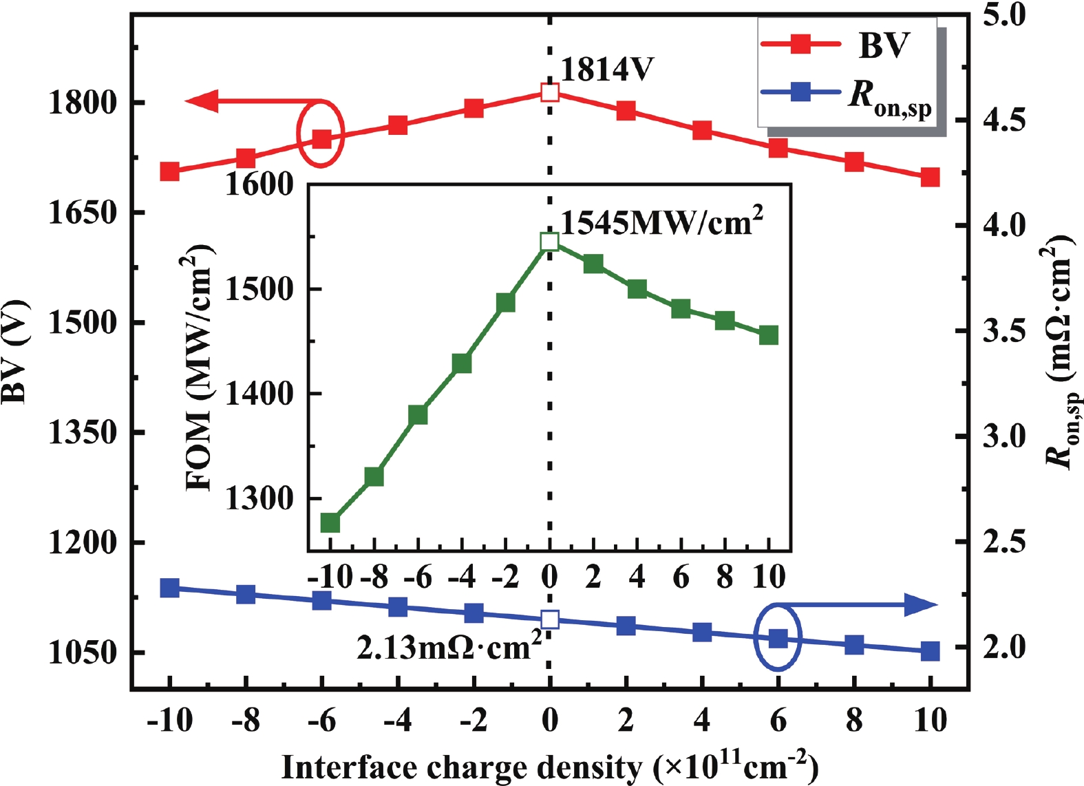
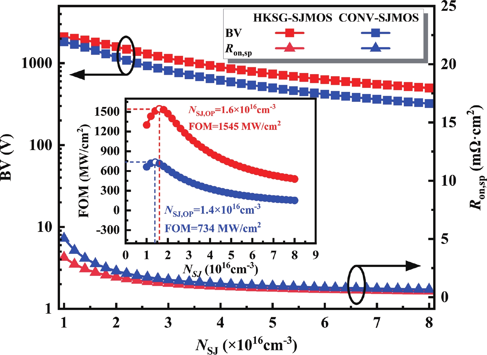
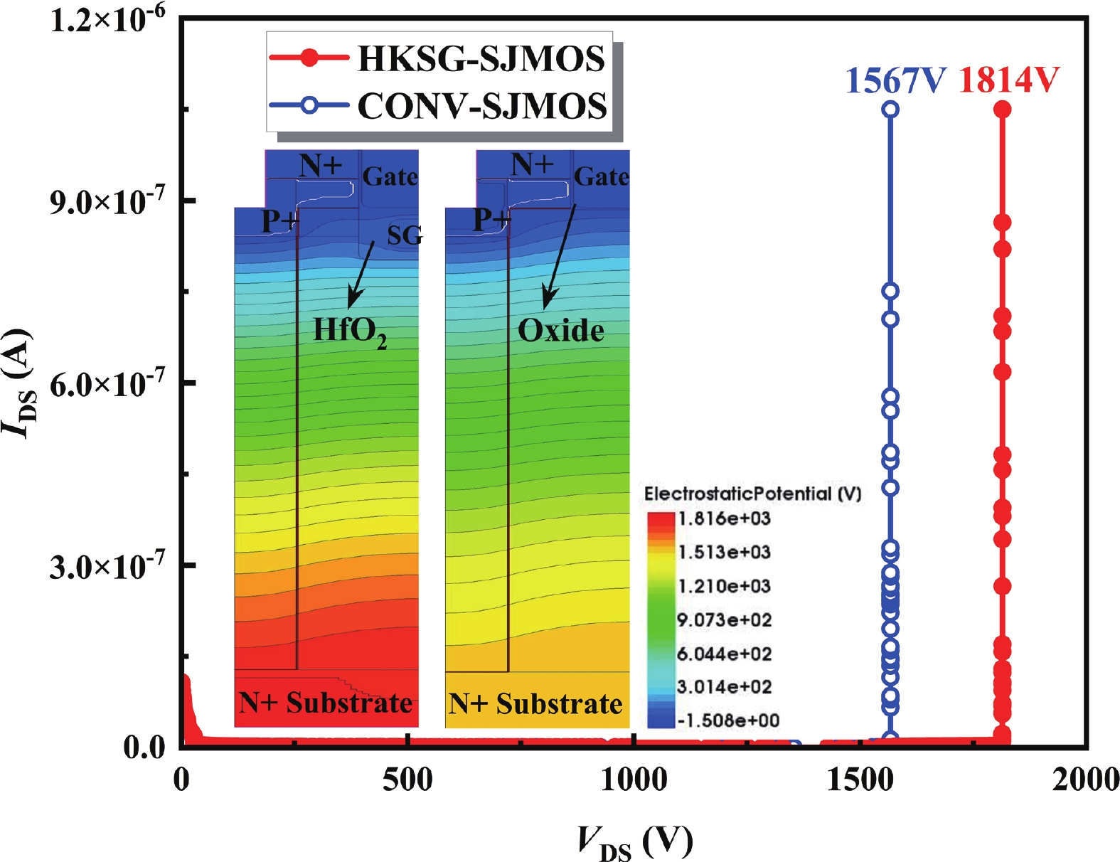
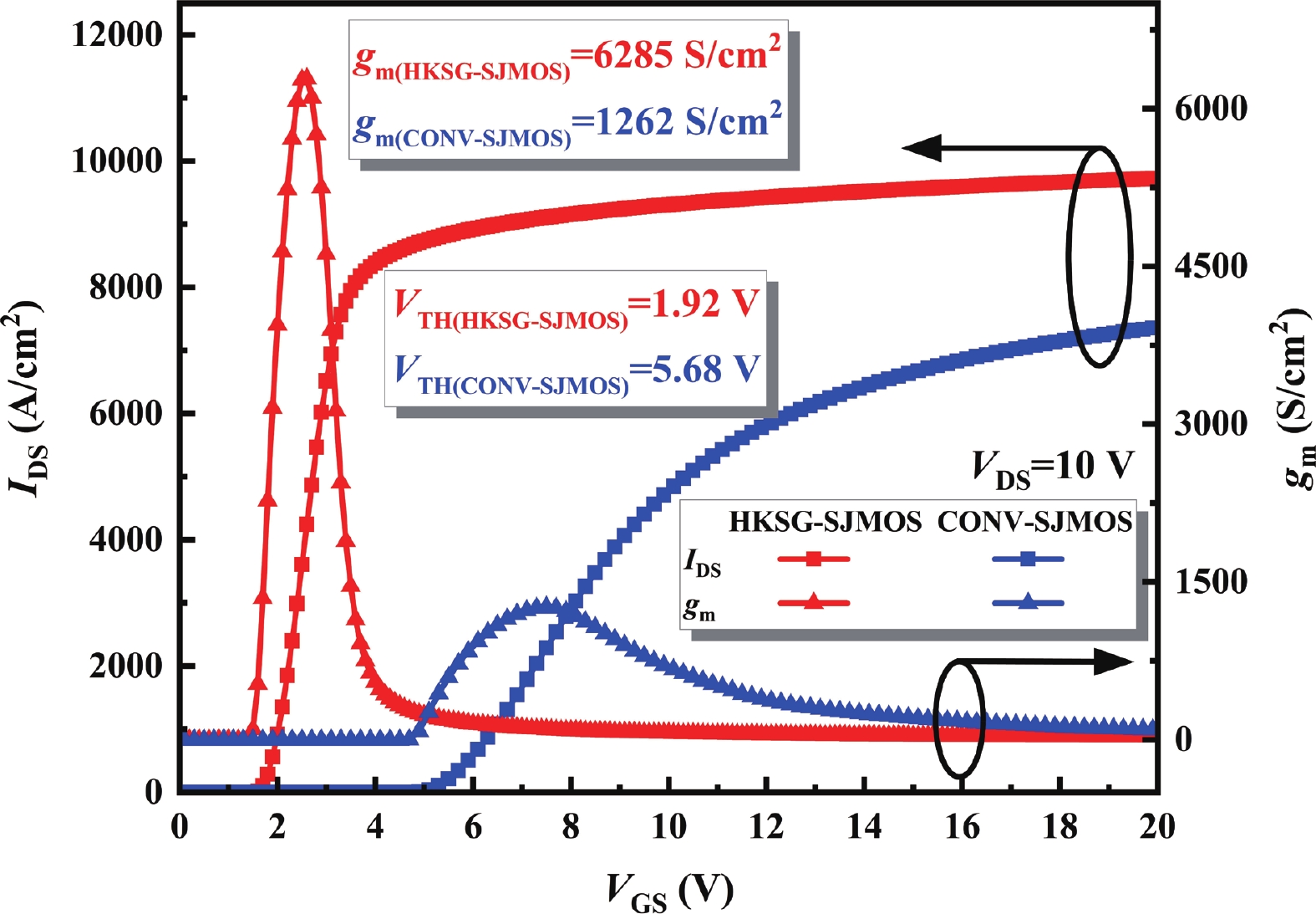
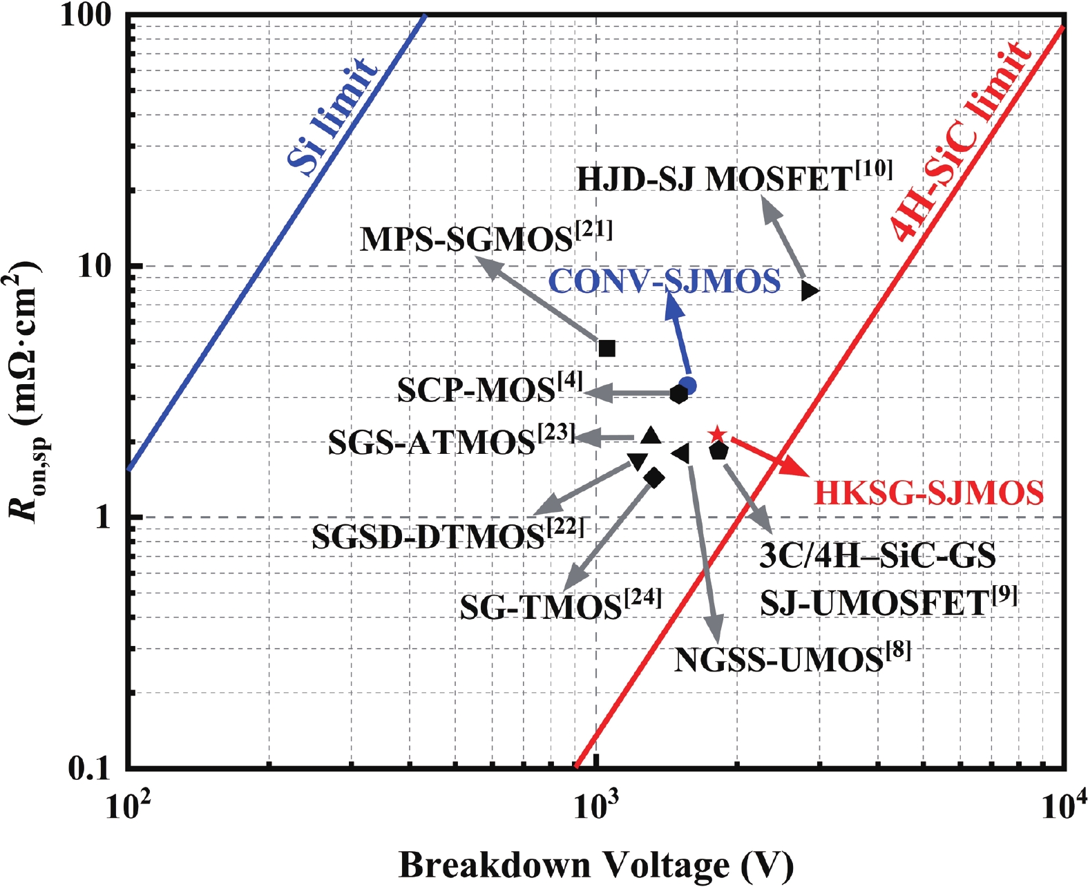
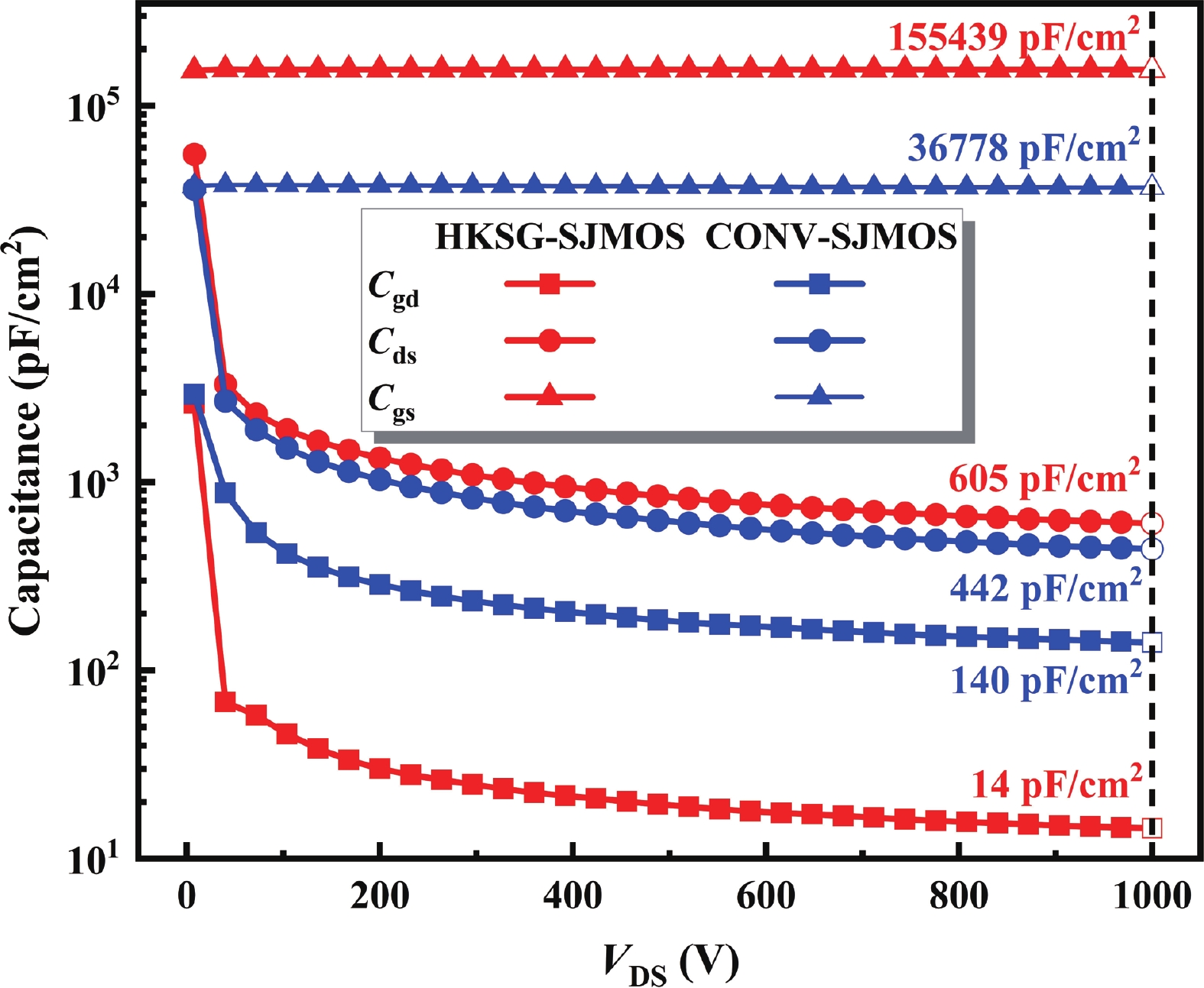
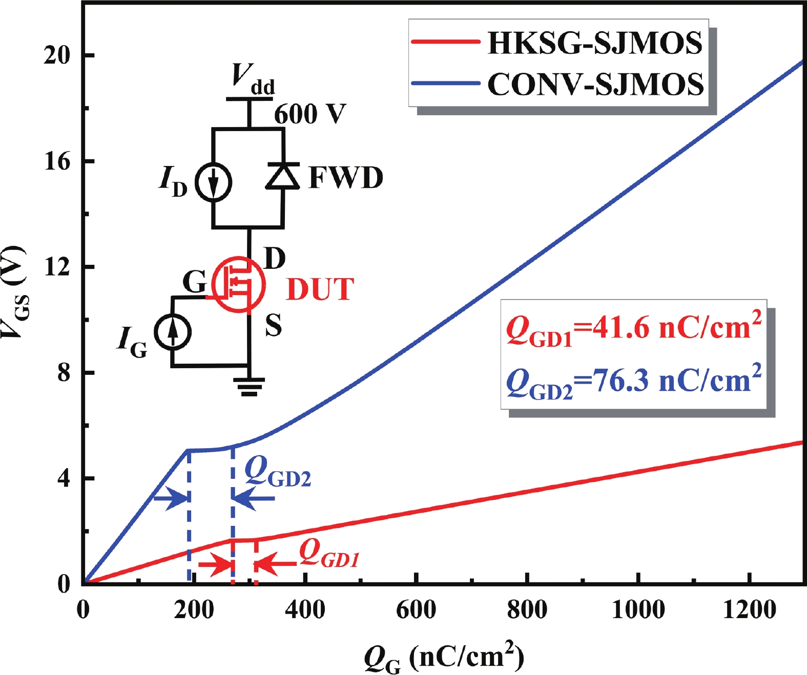
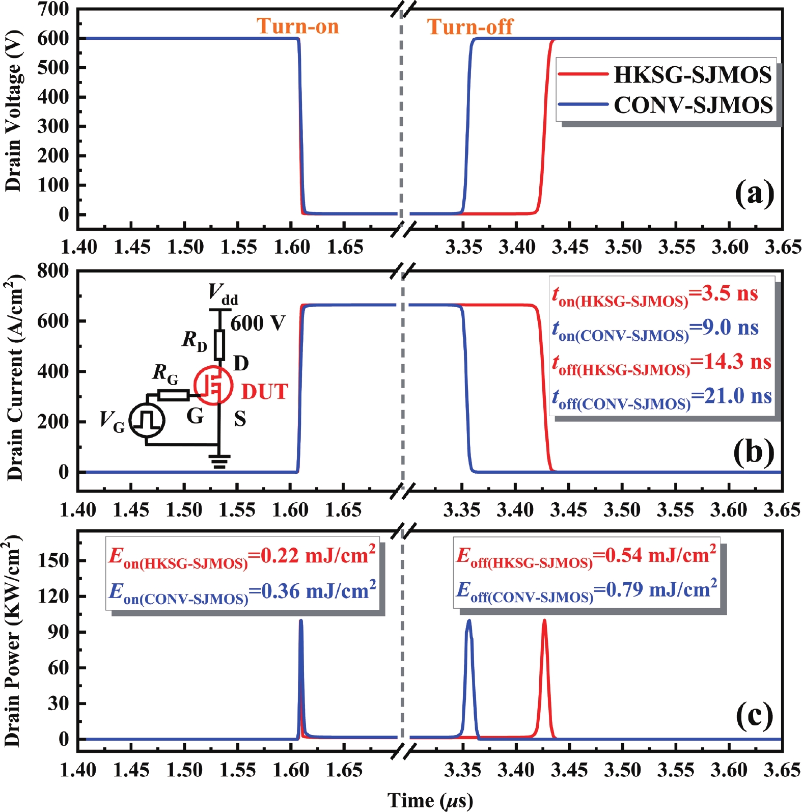
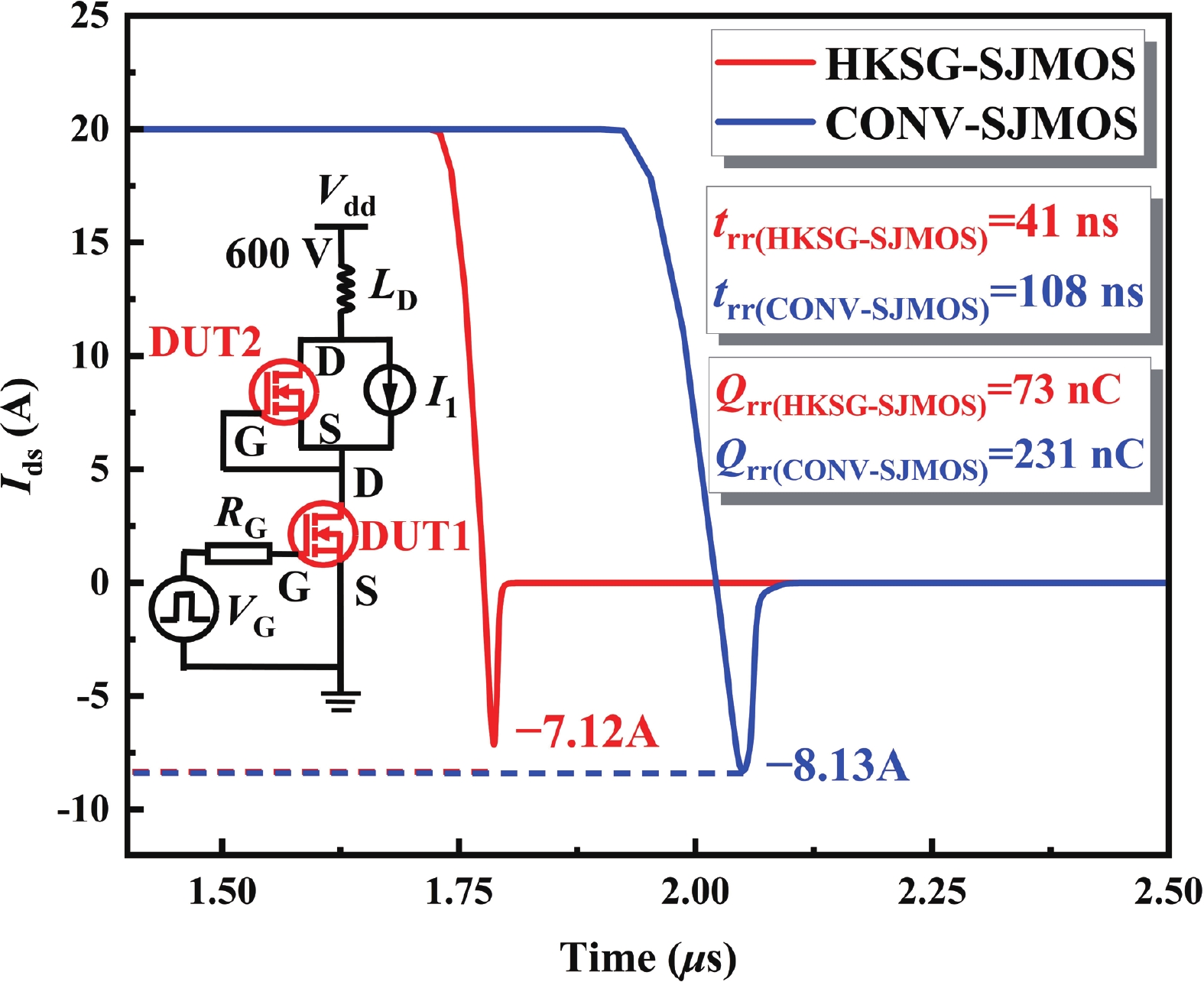
Table 1. Used parameters in the simulation.
| Parameters | HKSG- SJMOS |
CONV- SJMOS |
| P-drift width, Wp (µm) | 1 | 1 |
| N-drift width, Wd (µm) | 2 | 2 |
| High-K dielectric width, Whk (µm) | 1 | − |
| Split gate width, Wsg (µm) | 0.5 | − |
| Drift thickness, Td (µm) | 15 | 15 |
| Source trench thickness, Tst (µm) | 2 | 2 |
| Gate thickness, Tg (µm) | 2 | 2 |
| Split gate thickness, Tsg (µm) | 1 | − |
| Split gate dielectric thickness, Tsgdi (µm) | 0.4 | − |
| Gate dielectric thickness, Tdit (µm) | 0.4 | − |
| Relative permittivity, K | 25 | 3.9 |
| Superjunction region concentration, NSJ,OP (×1016 cm−3) |
1.6 | 1.4 |
| CSL concentration, NCSL (×1017 cm−3) | 1 | − |
| P-well concentration, NPW (×1017 cm−3) | 1 | 1 |
| Substrate concentration, NSUB (×1019 cm−3) | 1 | 1 |
 DownLoad: CSV
Table 2. Comparison of performance for the two devices and other reported devices.
| Parameters | HKSG-SJMOS | CONV-SJMOS | MPS-SGMOS[21] | SG-TMOS[24] |
| BV (V) | 1814 | 1567 | 1054 | 1322 |
| Ron,sp (mΩ·cm2) | 2.13 | 3.34 | 4.7 | 1.54 |
| FOM = BV2/Ron,sp (MW/cm2) | 1545 | 734 | 236 | 1134 |
| Eox,max (MV/cm) | 3.028 | 3.543 | 2.35 | 3.6 |
| VTH (V) | 1.92 | 5.68 | − | 1.87 |
| gm (S/cm2) | 6285 | 1262 | − | − |
| Cgd (pF/cm2) | 14 | 140 | 60 | 15 |
| HFFOM = Cgd · Ron,sp (mΩ·pF) | 29.82 | 467.6 | 282 | 23.1 |
| Qgd (nC/cm2) | 41.6 | 76.3 | 51 | 86 |
| HFFOM = Qgd · Ron,sp (mΩ·nC) | 88.608 | 254.842 | 239.7 | 132.44 |
DownLoad: CSV
Table 3. Comparison of performance for the two devices.
| Parameters | HKSG- SJMOS | CONV- SJMOS |
| Turn-on time, ton (ns) | 3.5 | 9.0 |
| Turn-off time, toff (ns) | 14.3 | 21.0 |
| Turn-on loss, Eon (mJ/cm2) | 0.22 | 0.36 |
| Turn-off loss, Eoff (mJ/cm2) | 0.54 | 0.79 |
| Peak reverse recovery current, Irrm (A) | −7.12 | −8.13 |
| Reverse recovery time, trr (ns) | 41 | 108 |
| Reverse recovery charge, Qrr (nC) | 73 | 231 |
DownLoad: CSV
| [1] |
Nan Y G, Han G Q. 4H–SiC floating junction Schottky barrier diode with compensation layer of engineered cathode structure: Cone–shaped electric field, current density waveform, and applications. Microelectron J, 2022, 125, 105472 doi: 10.1016/j.mejo.2022.105472
|
| [2] |
Luo M J, Zhang Y R, Wang Y C, et al. Design and modelling of SiC MPS diodes with superior surge current robustness. Microelectron J, 2024, 151, 106298 doi: 10.1016/j.mejo.2024.106298
|
| [3] |
Luo M J, Chen H, Zhang Y R, et al. Novel design and modelling of SiC junction barrier Schottky diode with improved Baliga FOM under high–temperature applications. Microelectron J, 2024, 151, 106343 doi: 10.1016/j.mejo.2024.106343
|
| [4] |
Wu L J, Yang G L, Yang D Q, et al. Self–clamped P–shield 4H–SiC trench MOSFET for low turn–off loss and suppress switching oscillation. Microelectron J, 2024, 151, 106307 doi: 10.1016/j.mejo.2024.106307
|
| [5] |
Harada S, Kobayashi Y, Kyogoku S, et al. First demonstration of dynamic characteristics for SiC superjunction MOSFET realized using multi–epitaxial growth method. 2018 IEEE International Electron Devices Meeting (IEDM), 2018, 8.2.1 doi: 10.1109/IEDM.2018.8614670
|
| [6] |
Kosugi R, Ji S Y, Mochizuki K, et al. Breaking the theoretical limit of 6.5 kV–class 4H–SiC super–junction (SJ) MOSFETs by trench–filling epitaxial growth. 2019 31st International Symposium on Power Semiconductor Devices and ICs (ISPSD), 2019, 39 doi: 10.1109/ISPSD.2019.8757632
|
| [7] |
Okada M, Kyogoku S, Kumazawa T, et al. Superior short–circuit performance of SiC superjunction MOSFET. 2020 32nd International Symposium on Power Semiconductor Devices and ICs (ISPSD), 2020, 70 doi: 10.1109/ISPSD46842.2020.9170126
|
| [8] |
Wang X J, Shen Z W, Zhang G L, et al. A 4H–SiC semi–super–junction shielded trench MOSFET: P–pillar is grounded to optimize the electric field characteristics. J Semicond, 2022, 43(12), 85 doi: 10.1088/1674-4926/43/12/122802
|
| [9] |
Ding J Y, Wei W S. An UMOSFET integrated with graded semi–super–junction and 3C/4H–SiC hetero–crystalline freewheeling junction. Microelectron J, 2023, 142, 105992 doi: 10.1016/j.mejo.2023.105992
|
| [10] |
Kim J, Kim K. A novel 4H–SiC super junction UMOSFET with heterojunction diode for enhanced reverse recovery characteristics. 2020 International Conference on Electronics, Information, and Communication (ICEIC) , 2020, 1 doi: 10.1109/ICEIC49074.2020.9051221
|
| [11] |
Yao J F, Yang Z F, Zhu Y Q, et al. Performance enhancement of 4H–SiC superjunction trench MOSFET with extended high–K dielectric. Microelectron J, 2024, 151, 106359 doi: 10.1016/j.mejo.2024.106359
|
| [12] |
Yao J F, Liu Y A, Li A, et al. Investigations of 4H–SiC trench MOSFET with integrated high–K deep trench and gate dielectric. IET Power Electron, 2024, 17(7), 869 doi: 10.1049/pel2.12700
|
| [13] |
Zheng Y L, Tang W M, Chau T, et al. Simulation study of 4H–SiC high–k pillar MOSFET with integrated Schottky barrier diode. IEEE J Electron Devices Soc, 2021, 9, 951 doi: 10.1109/JEDS.2021.3116715
|
| [14] |
Yao J F, Zhang Z Y, Guo Y F, et al. Novel LDMOS with integrated triple direction high–k gate and field dielectrics. IEEE Trans Electron Devices, 2021, 68(8), 3997 doi: 10.1109/TED.2021.3090352
|
| [15] |
Du L, Guo Y F, Zhang J, et al. The new structure and analytical model of a high–voltage interconnection shielding structure with high–k dielectric pillar. IEEE Trans Electron Devices, 2020, 67(4), 1745 doi: 10.1109/TED.2020.2975886
|
| [16] |
Wang Y, Lan H, Dou Z, et al. Method to improve trade–off performance for split–gate power U–shape metal–oxide semiconductor field–effect transistor with compound trench dielectrics. IET Power Electron, 2014, 7(8), 2030 doi: 10.1049/iet-pel.2013.0786
|
| [17] |
Huang L, Li X J, Sun Y B, et al. A novel split–gate trench MOSFET embedded with a high–k pillar for higher breakdown voltage. Semicond Sci Technol, 2024, 39(3), 035006 doi: 10.1088/1361-6641/ad1c62
|
| [18] |
Fang D, Yang G, Qiao M, et al. Split–gate trench metal–oxide–semiconductor field effect transistor with an inverted L–shaped source region. Microelectron J, 2022, 130, 105616 doi: 10.1016/j.mejo.2022.105616
|
| [19] |
Wang Z K, Qiao M, Li Z J, et al. Mechanisms and characteristics of a low–loss split gate trench MOSFET with shield layer. Microelectron J, 2021, 118, 105310 doi: 10.1016/j.mejo.2021.105310
|
| [20] |
Qiao M, Ma T, Dong S D, et al. A low gate charge field–plate trench MOSFET with hollow split gate structure. Microelectron J, 2022, 130, 105627 doi: 10.1016/j.mejo.2022.105627
|
| [21] |
Peng D S, Feng Q Y. A 4H–SiC double trench MOSFET with split gate and integrated MPS diode. Microelectron J, 2022, 128, 105553 doi: 10.1016/j.mejo.2022.105553
|
| [22] |
Zhang J P, Wu Q L, Chen Z X, et al. SiC double trench MOSFET with split gate and integrated Schottky barrier diode for ultra–low power loss and improved short–circuit capability. Chin J Electron, 2024, 33(5), 1127 doi: 10.23919/cje.2022.00.394
|
| [23] |
Zhang J P, Chen Z X, Tu Y Y, et al. A novel SiC asymmetric cell trench MOSFET with split gate and integrated JBS diode. IEEE J Electron Devices Soc, 2021, 9, 713 doi: 10.1109/JEDS.2021.3097390
|
| [24] |
Wu Z, Xia C, Yi B, et al. A split–gate SiC trench MOSFET with embedded unipolar diode for improved performances. 2021 IEEE 14th International Conference on ASIC (ASICON), 2021, 1 doi: 10.1109/ASICON52560.2021.9620233
|
| [25] |
Mahapatra S, De S, Joshi K, et al. Understanding process impact of hole traps and NBTI in HKMG p–MOSFETs using measurements and atomistic simulations. IEEE Electron Device Lett, 2013, 34(8), 963 doi: 10.1109/LED.2013.2270003
|


Article views: 1762 Times PDF downloads: 270 Times Cited by: 0 Times
Received: 08 January 2025 Revised: 20 February 2025 Online: Accepted Manuscript: 13 March 2025Uncorrected proof: 11 April 2025Published: 01 August 2025
| Citation: |
Jiafei Yao, Zhengfei Yang, Yuxuan Dai, Ziwei Hu, Man Li, Kemeng Yang, Jing Chen, Maolin Zhang, Jun Zhang, Yufeng Guo. 4H-SiC superjunction MOSFET with integrated high-K gate dielectric and split gate[J]. Journal of Semiconductors, 2025, 46(8): 082501. doi: 10.1088/1674-4926/25010005
****
J F Yao, Z F Yang, Y X Dai, Z W Hu, M Li, K M Yang, J Chen, M L Zhang, J Zhang, and Y F Guo, 4H-SiC superjunction MOSFET with integrated high-K gate dielectric and split gate[J]. J. Semicond., 2025, 46(8), 082501 doi: 10.1088/1674-4926/25010005

|
 Jiafei Yao received his Ph.D. degree in microelectronics and solid-state electronics from Nanjing University of Posts and Telecommunications. Currently, he is an associate professor in the Nanjing University of Posts and Telecommunications, Nanjing, China. His research focuses on the silicon power devices, silicon carbide power devices and power integrated circuits
 Zhengfei Yang received his bachelor's degree from Changzhou University in 2022. Now he is a graduate student at Nanjing University of Posts and Telecommunications under the supervision of Prof. Yufeng Guo and Prof. Jiafei Yao. He focuses on the research of silicon carbide power devices
 Yufeng Guo received his Ph.D. degree in microelectronics and solid-state electronics from the University of Electronic Science and Technology of China, Chengdu, China, in 2005. He is currently a professor in the Nanjing University of Posts and Telecommunications, Nanjing, China. He has authored over 150 SCI indexed papers, published 6 textbooks, and holds 73 granted patents. His current research interests include power devices, integration technology, RF-integrated circuit designs, and intelligent EDA/TCAD tools
| [1] |
Nan Y G, Han G Q. 4H–SiC floating junction Schottky barrier diode with compensation layer of engineered cathode structure: Cone–shaped electric field, current density waveform, and applications. Microelectron J, 2022, 125, 105472 doi: 10.1016/j.mejo.2022.105472
|
| [2] |
Luo M J, Zhang Y R, Wang Y C, et al. Design and modelling of SiC MPS diodes with superior surge current robustness. Microelectron J, 2024, 151, 106298 doi: 10.1016/j.mejo.2024.106298
|
| [3] |
Luo M J, Chen H, Zhang Y R, et al. Novel design and modelling of SiC junction barrier Schottky diode with improved Baliga FOM under high–temperature applications. Microelectron J, 2024, 151, 106343 doi: 10.1016/j.mejo.2024.106343
|
| [4] |
Wu L J, Yang G L, Yang D Q, et al. Self–clamped P–shield 4H–SiC trench MOSFET for low turn–off loss and suppress switching oscillation. Microelectron J, 2024, 151, 106307 doi: 10.1016/j.mejo.2024.106307
|
| [5] |
Harada S, Kobayashi Y, Kyogoku S, et al. First demonstration of dynamic characteristics for SiC superjunction MOSFET realized using multi–epitaxial growth method. 2018 IEEE International Electron Devices Meeting (IEDM), 2018, 8.2.1 doi: 10.1109/IEDM.2018.8614670
|
| [6] |
Kosugi R, Ji S Y, Mochizuki K, et al. Breaking the theoretical limit of 6.5 kV–class 4H–SiC super–junction (SJ) MOSFETs by trench–filling epitaxial growth. 2019 31st International Symposium on Power Semiconductor Devices and ICs (ISPSD), 2019, 39 doi: 10.1109/ISPSD.2019.8757632
|
| [7] |
Okada M, Kyogoku S, Kumazawa T, et al. Superior short–circuit performance of SiC superjunction MOSFET. 2020 32nd International Symposium on Power Semiconductor Devices and ICs (ISPSD), 2020, 70 doi: 10.1109/ISPSD46842.2020.9170126
|
| [8] |
Wang X J, Shen Z W, Zhang G L, et al. A 4H–SiC semi–super–junction shielded trench MOSFET: P–pillar is grounded to optimize the electric field characteristics. J Semicond, 2022, 43(12), 85 doi: 10.1088/1674-4926/43/12/122802
|
| [9] |
Ding J Y, Wei W S. An UMOSFET integrated with graded semi–super–junction and 3C/4H–SiC hetero–crystalline freewheeling junction. Microelectron J, 2023, 142, 105992 doi: 10.1016/j.mejo.2023.105992
|
| [10] |
Kim J, Kim K. A novel 4H–SiC super junction UMOSFET with heterojunction diode for enhanced reverse recovery characteristics. 2020 International Conference on Electronics, Information, and Communication (ICEIC) , 2020, 1 doi: 10.1109/ICEIC49074.2020.9051221
|
| [11] |
Yao J F, Yang Z F, Zhu Y Q, et al. Performance enhancement of 4H–SiC superjunction trench MOSFET with extended high–K dielectric. Microelectron J, 2024, 151, 106359 doi: 10.1016/j.mejo.2024.106359
|
| [12] |
Yao J F, Liu Y A, Li A, et al. Investigations of 4H–SiC trench MOSFET with integrated high–K deep trench and gate dielectric. IET Power Electron, 2024, 17(7), 869 doi: 10.1049/pel2.12700
|
| [13] |
Zheng Y L, Tang W M, Chau T, et al. Simulation study of 4H–SiC high–k pillar MOSFET with integrated Schottky barrier diode. IEEE J Electron Devices Soc, 2021, 9, 951 doi: 10.1109/JEDS.2021.3116715
|
| [14] |
Yao J F, Zhang Z Y, Guo Y F, et al. Novel LDMOS with integrated triple direction high–k gate and field dielectrics. IEEE Trans Electron Devices, 2021, 68(8), 3997 doi: 10.1109/TED.2021.3090352
|
| [15] |
Du L, Guo Y F, Zhang J, et al. The new structure and analytical model of a high–voltage interconnection shielding structure with high–k dielectric pillar. IEEE Trans Electron Devices, 2020, 67(4), 1745 doi: 10.1109/TED.2020.2975886
|
| [16] |
Wang Y, Lan H, Dou Z, et al. Method to improve trade–off performance for split–gate power U–shape metal–oxide semiconductor field–effect transistor with compound trench dielectrics. IET Power Electron, 2014, 7(8), 2030 doi: 10.1049/iet-pel.2013.0786
|
| [17] |
Huang L, Li X J, Sun Y B, et al. A novel split–gate trench MOSFET embedded with a high–k pillar for higher breakdown voltage. Semicond Sci Technol, 2024, 39(3), 035006 doi: 10.1088/1361-6641/ad1c62
|
| [18] |
Fang D, Yang G, Qiao M, et al. Split–gate trench metal–oxide–semiconductor field effect transistor with an inverted L–shaped source region. Microelectron J, 2022, 130, 105616 doi: 10.1016/j.mejo.2022.105616
|
| [19] |
Wang Z K, Qiao M, Li Z J, et al. Mechanisms and characteristics of a low–loss split gate trench MOSFET with shield layer. Microelectron J, 2021, 118, 105310 doi: 10.1016/j.mejo.2021.105310
|
| [20] |
Qiao M, Ma T, Dong S D, et al. A low gate charge field–plate trench MOSFET with hollow split gate structure. Microelectron J, 2022, 130, 105627 doi: 10.1016/j.mejo.2022.105627
|
| [21] |
Peng D S, Feng Q Y. A 4H–SiC double trench MOSFET with split gate and integrated MPS diode. Microelectron J, 2022, 128, 105553 doi: 10.1016/j.mejo.2022.105553
|
| [22] |
Zhang J P, Wu Q L, Chen Z X, et al. SiC double trench MOSFET with split gate and integrated Schottky barrier diode for ultra–low power loss and improved short–circuit capability. Chin J Electron, 2024, 33(5), 1127 doi: 10.23919/cje.2022.00.394
|
| [23] |
Zhang J P, Chen Z X, Tu Y Y, et al. A novel SiC asymmetric cell trench MOSFET with split gate and integrated JBS diode. IEEE J Electron Devices Soc, 2021, 9, 713 doi: 10.1109/JEDS.2021.3097390
|
| [24] |
Wu Z, Xia C, Yi B, et al. A split–gate SiC trench MOSFET with embedded unipolar diode for improved performances. 2021 IEEE 14th International Conference on ASIC (ASICON), 2021, 1 doi: 10.1109/ASICON52560.2021.9620233
|
| [25] |
Mahapatra S, De S, Joshi K, et al. Understanding process impact of hole traps and NBTI in HKMG p–MOSFETs using measurements and atomistic simulations. IEEE Electron Device Lett, 2013, 34(8), 963 doi: 10.1109/LED.2013.2270003
|

 WeChat ID
Journal of Semiconductors © 2017 All Rights Reserved 京ICP备05085259号-2


