


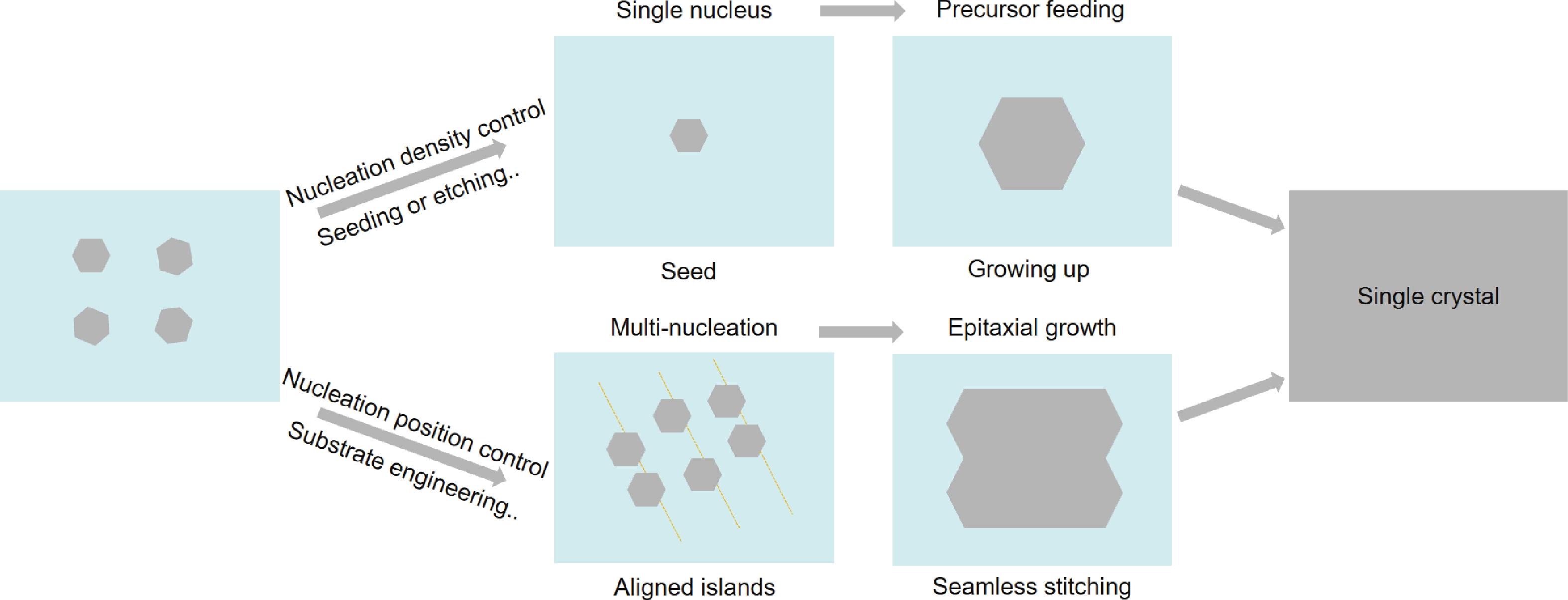
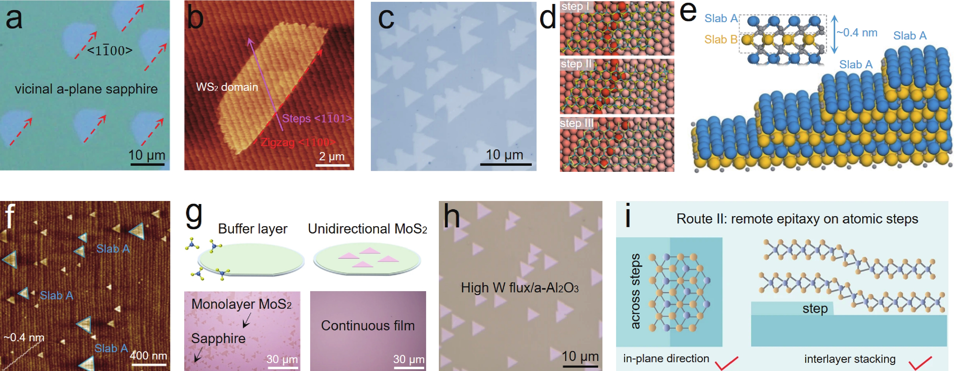
Fig. 1.
(Color online) Schematic diagram of two strategies for the epitaxial growth of single-crystal 2D materials.
REVIEWS
Jinxia Bai1, 2, §, Chi Zhang1, 2, §, Fankai Zeng1, 2, Jinzong Kou1, 2, Jinhuan Wang1, 2, and Xiaozhi Xu1, 2,
Corresponding author: Jinhuan Wang, jinhuanwang@scnu.edu.cn; Xiaozhi Xu, xiaozhixu@scnu.edu.cn
Abstract: The unique structure and exceptional properties of two-dimensional (2D) materials offer significant potential for transformative advancements in semiconductor industry. Similar to the reliance on wafer-scale single-crystal ingots for silicon-based chips, practical applications of 2D materials at the chip level need large-scale, high-quality production of 2D single crystals. Over the past two decades, the size of 2D single-crystals has been improved to wafer or meter scale, where the nucleation control during the growth process is particularly important. Therefore, it is essential to conduct a comprehensive review of nucleation control to gain fundamental insights into the growth of 2D single-crystal materials. This review mainly focuses on two aspects: controlling nucleation density to enable the growth from a single nucleus, and controlling nucleation position to achieve the unidirectionally aligned islands and subsequent seamless stitching. Finally, we provide an overview and forecast of the strategic pathways for emerging 2D materials.
Key words: 2D materials, single crystals, nucleation density, nucleation position
| [1] |
Morton J J L, McCamey D R, Eriksson M A, et al. Embracing the quantum limit in silicon computing. Nature, 2011, 479(7373), 345 doi: 10.1038/nature10681
|
| [2] |
Ferain I, Colinge C A, Colinge J P. Multigate transistors as the future of classical metal-oxide-semiconductor field-effect transistors. Nature, 2011, 479(7373), 310 doi: 10.1038/nature10676
|
| [3] |
Ionescu A M, Riel H. Tunnel field-effect transistors as energy-efficient electronic switches. Nature, 2011, 479(7373), 329 doi: 10.1038/nature10679
|
| [4] |
Theis T N, Solomon P M. It's time to reinvent the transistor! Science, 2010, 327(5973), 1600
|
| [5] |
Lundstrom M. Moore's law forever? Science, 2003, 299(5604), 210 doi: 10.1126/science.1079567
|
| [6] |
Castellanos-Gomez A. Why all the fuss about 2D semiconductors? Nat Photonics, 2016, 10(4), 202 doi: 10.1038/nphoton.2016.53
|
| [7] |
Mounet N, Gibertini M, Schwaller P, et al. Two-dimensional materials from high-throughput computational exfoliation of experimentally known compounds. Nat Nanotechnol, 2018, 13(3), 246 doi: 10.1038/s41565-017-0035-5
|
| [8] |
Novoselov K S, Geim A K, Morozov S V, et al. Electric field effect in atomically thin carbon films. Science, 2004, 306(5696), 666 doi: 10.1126/science.1102896
|
| [9] |
Li X, Cai W, An J, et al. Large-area synthesis of high-quality and uniform graphene films on copper foils. Science, 2009, 324(5932), 1312 doi: 10.1126/science.1171245
|
| [10] |
Desai S B, Madhvapathy S R, Sachid A B, et al. MoS2 transistors with 1-nanometer gate lengths. Science, 2016, 354(6308), 99 doi: 10.1126/science.aah4698
|
| [11] |
Chhowalla M, Shin H S, Eda G, et al. The chemistry of two-dimensional layered transition metal dichalcogenide nanosheets. Nat Chem, 2013, 5(4), 263 doi: 10.1038/nchem.1589
|
| [12] |
Song L, Ci L J, Lu H, et al. Large scale growth and characterization of atomic hexagonal boron nitride layers. Nano Lett, 2010, 10(8), 3209 doi: 10.1021/nl1022139
|
| [13] |
Shi Y, Hamsen C, Jia X, et al. Synthesis of few-layer hexagonal boron nitride thin film by chemical vapor deposition. Nano Lett, 2010, 10(10), 4134 doi: 10.1021/nl1023707
|
| [14] |
Wu R T, Drozdov I K, Eltinge S, et al. Large-area single-crystal sheets of borophene on Cu(111) surfaces. Nat Nanotechnol, 2019, 14(1), 44 doi: 10.1038/s41565-018-0317-6
|
| [15] |
Chen C, Yin Y L, Zhang R C, et al. Growth of single-crystal black phosphorus and its alloy films through sustained feedstock release. Nat Mater, 2023, 22(6), 717 doi: 10.1038/s41563-023-01516-1
|
| [16] |
Zhou Z Q, Shen T, Wang P, et al. Low symmetric sub-wavelength array enhanced lensless polarization- sensitivity photodetector of germanium selenium. Sci Bull, 2023, 68(2), 173 doi: 10.1016/j.scib.2023.01.013
|
| [17] |
Weber B, Fuhrer M S, Sheng X L, et al. 2024 roadmap on 2D topological insulators. J Phys Mater, 2024, 7(2), 022501 doi: 10.1088/2515-7639/ad2083
|
| [18] |
Lin Y C, Torsi R, Younas R, et al. Recent advances in 2D material theory, synthesis, properties, and applications. ACS Nano, 2023, 17(11), 9694 doi: 10.1021/acsnano.2c12759
|
| [19] |
Barja S, Refaely-Abramson S, Schuler B, et al. Identifying substitutional oxygen as a prolific point defect in monolayer transition metal dichalcogenides. Nat Commun, 2019, 10(1), 3382 doi: 10.1038/s41467-019-11342-2
|
| [20] |
Rhodes D, Chae S H, Ribeiro-Palau R, et al. Disorder in van der Waals heterostructures of 2D materials. Nat Mater, 2019, 18(6), 541 doi: 10.1038/s41563-019-0366-8
|
| [21] |
Yao W, Wu B, Liu Y. Growth and grain boundaries in 2D materials. ACS Nano, 2020, 14(8), 9320 doi: 10.1021/acsnano.0c03558
|
| [22] |
Hämäläinen J, Mattinen M, Mizohata K, et al. Atomic layer deposition of rhenium disulfide. Adv Mater, 2018, 30(24), 1703622 doi: 10.1002/adma.201703622
|
| [23] |
Parker M. Oxide dielectrics that grow on 2D materials. Nat Electron, 2024, 7(7), 513 doi: 10.1038/s41928-024-01221-0
|
| [24] |
Cai J Y, Han X X, Wang X, et al. Atomic layer deposition of two-dimensional layered materials: processes, growth mechanisms, and characteristics. Matter, 2020, 2(3), 587 doi: 10.1016/j.matt.2019.12.026
|
| [25] |
Liu Z L, Wu X, Shao Y, et al. Epitaxially grown monolayer VSe2: an air-stable magnetic two-dimensional material with low work function at edges. Sci Bull, 2018, 63(7), 419 doi: 10.1016/j.scib.2018.03.008
|
| [26] |
Poh S M, Zhao X X, Tan S J R, et al. Molecular beam epitaxy of highly crystalline MoSe2 on hexagonal boron nitride. ACS Nano, 2018, 12(8), 7562 doi: 10.1021/acsnano.8b04037
|
| [27] |
Chen M W, Ovchinnikov D, Lazar S, et al. Highly oriented atomically thin ambipolar MoSe2 grown by molecular beam epitaxy. ACS Nano, 2017, 11(6), 6355 doi: 10.1021/acsnano.7b02726
|
| [28] |
Ma K Y, Zhang L, Jin S, et al. Epitaxial single-crystal hexagonal boron nitride multilayers on Ni (111). Nature, 2022, 606(7912), 88 doi: 10.1038/s41586-022-04745-7
|
| [29] |
Dai Z H, Liu L Q, Zhang Z. Strain engineering of 2D materials: Issues and opportunities at the interface. Adv Mater, 2019, 31(45), 1805417 doi: 10.1002/adma.201805417
|
| [30] |
Aljarb A, Cao Z, Tang H L, et al. Substrate lattice-guided seed formation controls the orientation of 2D transition-metal dichalcogenides. ACS Nano, 2017, 11(9), 9215 doi: 10.1021/acsnano.7b04323
|
| [31] |
Li P F, Kang Z, Zhang Z, et al. In situ microscopy techniques for characterizing the mechanical properties and deformation behavior of two-dimensional (2D) materials. Mater Today, 2021, 51, 247 doi: 10.1016/j.mattod.2021.10.009
|
| [32] |
Ismach A, Druzgalski C, Penwell S, et al. Direct chemical vapor deposition of graphene on dielectric surfaces. Nano Lett, 2010, 10(5), 1542 doi: 10.1021/nl9037714
|
| [33] |
Pang J B, Mendes R G, Wrobel P S, et al. Self-terminating confinement approach for large-area uniform monolayer graphene directly over Si/SiOX by chemical vapor deposition. ACS Nano, 2017, 11(2), 1946 doi: 10.1021/acsnano.6b08069
|
| [34] |
Tang S J, Wang H M, Wang H S, et al. Silane-catalysed fast growth of large single-crystalline graphene on hexagonal boron nitride. Nat Commun, 2015, 6(1), 6499 doi: 10.1038/ncomms7499
|
| [35] |
Kato T, Hatakeyama R. Direct growth of doping-density-controlled hexagonal graphene on SiO2 substrate by rapid-heating plasma CVD. ACS Nano, 2012, 6(10), 8508 doi: 10.1021/nn302290z
|
| [36] |
Jang A R, Hong S, Hyun C, et al. Wafer-scale and wrinkle-free epitaxial growth of single-orientated multilayer hexagonal boron nitride on sapphire. Nano Lett, 2016, 16(5), 3360 doi: 10.1021/acs.nanolett.6b01051
|
| [37] |
Shi Z Y, Wang X J, Li Q T, et al. Vapor-liquid-solid growth of large-area multilayer hexagonal boron nitride on dielectric substrates. Nat Commun, 2020, 11(849), 90 doi: 10.1038/s41467-019-13858-z
|
| [38] |
Zhou J D, Lin J H, Huang X W, et al. A library of atomically thin metal chalcogenides. Nature, 2018, 556(7701), 355 doi: 10.1038/s41586-018-0008-3
|
| [39] |
Wu T R, Zhang X F, Yuan Q H, et al. Fast growth of inch-sized single-crystalline graphene from a controlled single nucleus on Cu-Ni alloys. Nat Mater, 2016, 15(1), 43 doi: 10.1038/nmat4477
|
| [40] |
Xu X Z, Zhang Z H, Dong J C, et al. Ultrafast epitaxial growth of metre-sized single-crystal graphene on industrial Cu foil. Sci Bull, 2017, 62(15), 1074 doi: 10.1016/j.scib.2017.07.005
|
| [41] |
Deng B, Xin Z W, Xue R W, et al. Scalable and ultrafast epitaxial growth of single-crystal graphene wafers for electrically tunable liquid-crystal microlens arrays. Sci Bull, 2019, 64(10), 659 doi: 10.1016/j.scib.2019.04.030
|
| [42] |
Wang L, Xu X Z, Zhang L N, et al. Epitaxial growth of a 100-square-centimetre single-crystal hexagonal boron nitride monolayer on copper. Nature, 2019, 570(7759), 91 doi: 10.1038/s41586-019-1226-z
|
| [43] |
Yang P F, Zhang S Q, Pan S Y, et al. Epitaxial growth of centimeter-scale single-crystal MoS2 monolayer on Au(111). ACS Nano, 2020, 14(4), 5036 doi: 10.1021/acsnano.0c01478
|
| [44] |
Wang J H, Xu X Z, Cheng T, et al. Dual-coupling-guided epitaxial growth of wafer-scale single-crystal WS2 monolayer on vicinal a-plane sapphire. Nat Nanotechnol, 2022, 17(1), 33 doi: 10.1038/s41565-021-01004-0
|
| [45] |
Chen T A, Chuu C P, Tseng C C, et al. Wafer-scale single-crystal hexagonal boron nitride monolayers on Cu (111). Nature, 2020, 579(7798), 219 doi: 10.1038/s41586-020-2009-2
|
| [46] |
Lin L, Li J Y, Ren H Y, et al. Surface engineering of copper foils for growing centimeter-sized single-crystalline graphene. ACS Nano, 2016, 10(2), 2922 doi: 10.1021/acsnano.6b00041
|
| [47] |
Yan Z, Lin J, Peng Z W, et al. Toward the synthesis of wafer-scale single-crystal graphene on copper foils. ACS Nano, 2012, 6(10), 9110 doi: 10.1021/nn303352k
|
| [48] |
Ding D, Solís-Fernández P, Hibino H, et al. Spatially controlled nucleation of single crystal graphene on Cu assisted by stacked Ni. ACS Nano, 2016, 10(12), 11196 doi: 10.1021/acsnano.6b06265
|
| [49] |
Zhou H L, Yu W J, Liu L X, et al. Chemical vapour deposition growth of large single crystals of monolayer and bilayer graphene. Nat Commun, 2013, 4(1), 2096 doi: 10.1038/ncomms3096
|
| [50] |
Li J, Wang X Y, Liu X R, et al. Facile growth of centimeter-sized single-crystal graphene on copper foil at atmospheric pressure. J Mater Chem C, 2015, 3(15), 3530 doi: 10.1039/C5TC00235D
|
| [51] |
Mohsin A, Liu L, Liu P Z, et al. Synthesis of millimeter-size hexagon-shaped graphene single crystals on resolidified copper. ACS Nano, 2013, 7(10), 8924 doi: 10.1021/nn4034019
|
| [52] |
Hao Y F, Bharathi M S, Wang L, et al. The role of surface oxygen in the growth of large single-crystal graphene on copper. Science, 2013, 342(6159), 720 doi: 10.1126/science.1243879
|
| [53] |
Vlassiouk I V, Stehle Y, Pudasaini P R, et al. Evolutionary selection growth of two-dimensional materials on polycrystalline substrates. Nat Mater, 2018, 17(4), 318 doi: 10.1038/s41563-018-0019-3
|
| [54] |
Xu X Z, Zhang Z H, Qiu L, et al. Ultrafast growth of single-crystal graphene assisted by a continuous oxygen supply. Nat Nanotechnol, 2016, 11(11), 930 doi: 10.1038/nnano.2016.132
|
| [55] |
Chia X Y, Pumera M. Characteristics and performance of two-dimensional materials for electrocatalysis. Nat Catal, 2018, 1(12), 909 doi: 10.1038/s41929-018-0181-7
|
| [56] |
Daus A, Vaziri S, Chen V, et al. High-performance flexible nanoscale transistors based on transition metal dichalcogenides. Nat Electron, 2021, 4(7), 495 doi: 10.1038/s41928-021-00598-6
|
| [57] |
Xing Z, Xiaozong H, Jing Y, et al. 2D layered material-based van der Waals heterostructures for optoelectronics. Adv Funct Materials, 2023, 33(18), 1 doi: 10.1002/adfm.201706587
|
| [58] |
An J R, Zhao X Y, Zhang Y N, et al. Perspectives of 2D materials for optoelectronic integration. Adv Funct Materials, 2022, 32(14), 24 doi: 10.1002/adfm.202110119
|
| [59] |
Liang G Z, Yu X C, Hu X N, et al. Mid-infrared photonics and optoelectronics in 2D materials. Mater Today, 2021, 51, 294 doi: 10.1016/j.mattod.2021.09.021
|
| [60] |
Zhou G, Ji J, Chen Z, et al. Scalable electronic and optoelectronic devices based on 2D TMDs. Materials Futures, 2024, 3(4), 042701 doi: 10.1088/2752-5724/ad7c6c
|
| [61] |
Qiu H, Yu Z, Zhao T, et al. Two-dimensional materials for future information technology: status and prospects. Sci China Inf Sci, 2024, 67(6), 160400 doi: 10.1007/s11432-024-4033-8
|
| [62] |
Xu X L, Pan Y, Liu S, et al. Seeded 2D epitaxy of large-area single-crystal films of the van der Waals semiconductor 2H MoTe2. Science, 2021, 372(6538), 195 doi: 10.1126/science.abf5825
|
| [63] |
Suzuki H, Hashimoto R, Misawa M, et al. Surface diffusion-limited growth of large and high-quality monolayer transition metal dichalcogenides in confined space of microreactor. ACS Nano, 2022, 16(7), 11360 doi: 10.1021/acsnano.2c05076
|
| [64] |
Zhang Z W, Chen P, Yang X D, et al. Ultrafast growth of large single crystals of monolayer WS2 and WSe2. Natl Sci Rev, 2020, 7(4), 737 doi: 10.1093/nsr/nwz223
|
| [65] |
Jiang H, Zhang X, Chen K, et al. Two-dimensional Czochralski growth of single-crystal MoS2. Nat Mater, 2025, 24(2), 188 doi: 10.1038/s41563-024-02069-7
|
| [66] |
Abbas A, Luo Y J, Ahmad W, et al. Recent progress, challenges, and opportunities in 2D materials for flexible displays. Nano Today, 2024, 56, 102256 doi: 10.1016/j.nantod.2024.102256
|
| [67] |
Yang L S, Chen W J, Yu Q M, et al. Mass production of two-dimensional materials beyond graphene and their applications. Nano Res, 2021, 14(6), 1583 doi: 10.1007/s12274-020-2897-3
|
| [68] |
Song X J, Gao J F, Nie Y F, et al. Chemical vapor deposition growth of large-scale hexagonal boron nitride with controllable orientation. Nano Res, 2015, 8(10), 3164 doi: 10.1007/s12274-015-0816-9
|
| [69] |
Liu L N, Wu J X, Wu L Y, et al. Phase-selective synthesis of 1T′ MoS2 monolayers and heterophase bilayers. Nat Mater, 2018, 17(12), 1108 doi: 10.1038/s41563-018-0187-1
|
| [70] |
Ruzmetov D, Zhang K, Stan G, et al. Vertical 2D/3D semiconductor heterostructures based on epitaxial molybdenum disulfide and gallium nitride. ACS Nano, 2016, 10(3), 3580 doi: 10.1021/acsnano.5b08008
|
| [71] |
Zhu H, Nayir N, Choudhury T H, et al. Step engineering for nucleation and domain orientation control in WSe2 epitaxy on c-plane sapphire. Nat Nanotechnol, 2023, 18(11), 1295 doi: 10.1038/s41565-023-01456-6
|
| [72] |
Yang P, Wang D, Zhao X, et al. Epitaxial growth of inch-scale single-crystal transition metal dichalcogenides through the patching of unidirectionally orientated ribbons. Nat Commun, 2022, 13(1), 3238 doi: 10.1038/s41467-022-30900-9
|
| [73] |
Wu M, Zhang Z, Xu X, et al. Seeded growth of large single-crystal copper foils with high-index facets. Nature, 2020, 581(7809), 406 doi: 10.1038/s41586-020-2298-5
|
| [74] |
Li Y L Z, Sun L Z, Chang Z H, et al. Large single-crystal cu foils with high-index facets by strain-engineered anomalous grain growth. Adv Mater, 2020, 32(29), 7 doi: 10.1002/adma.202002034
|
| [75] |
Hou Y T, Wang B J, Zhan L L, et al. Surface crystallographic structure insensitive growth of oriented graphene domains on Cu substrates. Mater Today, 2020, 36, 10 doi: 10.1016/j.mattod.2019.12.001
|
| [76] |
Lee J H, Lee E K, Joo W J, et al. Wafer-scale growth of single-crystal monolayer graphene on reusable hydrogen-terminated germanium. Science, 2014, 344(6181), 286 doi: 10.1126/science.1252268
|
| [77] |
Li P L, Wei W Y, Zhang M, et al. Wafer-scale growth of single-crystal graphene on vicinal Ge(001) substrate. Nano Today, 2020, 34, 100908 doi: 10.1016/j.nantod.2020.100908
|
| [78] |
Kang H, Tang P T, Shu H B, et al. Epitaxial growth of wafer scale antioxidant single-crystal graphene on twinned Pt(111). Carbon, 2021, 181, 225 doi: 10.1016/j.carbon.2021.05.027
|
| [79] |
Zhao T E, Guo J X, Li T T, et al. Substrate engineering for wafer-scale two-dimensional material growth: strategies, mechanisms, and perspectives. Chem Soc Rev, 2023, 52(5), 1650 doi: 10.1039/D2CS00657J
|
| [80] |
Nguyen V L, Shin B G, Duong D L, et al. Seamless stitching of graphene domains on polished copper (111) foil. Adv Mater, 2015, 27(8), 1376 doi: 10.1002/adma.201404541
|
| [81] |
Hu B S, Ago H, Ito Y, et al. Epitaxial growth of large-area single-layer graphene over Cu(111)/sapphire by atmospheric pressure CVD. Carbon, 2012, 50(1), 57 doi: 10.1016/j.carbon.2011.08.002
|
| [82] |
Nai C T, Xu H, Tan S J R, et al. Analyzing dirac cone and phonon dispersion in highly oriented nanocrystalline graphene. ACS Nano, 2016, 10(1), 1681 doi: 10.1021/acsnano.5b07662
|
| [83] |
Gao L B, Xu H, Li L J, et al. Heteroepitaxial growth of wafer scale highly oriented graphene using inductively coupled plasma chemical vapor deposition. 2D Mater, 2016, 3(2), 021001 doi: 10.1088/2053-1583/3/2/021001
|
| [84] |
Wang X L, Yuan Q H, Li J, et al. The transition metal surface dependent methane decomposition in graphene chemical vapor deposition growth. Nanoscale, 2017, 9(32), 11584 doi: 10.1039/C7NR02743E
|
| [85] |
Liu Y F, Wu T R, Yin Y L, et al. How low nucleation density of graphene on CuNi alloy is achieved. Adv Sci, 2018, 5(6), 8 doi: 10.1002/advs.201700961
|
| [86] |
Walsh L A, Hinkle C L. van der Waals epitaxy: 2D materials and topological insulators. Appl Mater Today, 2017, 9, 504 doi: 10.1016/j.apmt.2017.09.010
|
| [87] |
Liu C, Liu T Y, Zhang Z B, et al. Understanding epitaxial growth of two-dimensional materials and their homostructures. Nat Nanotechnol, 2024, 19(7), 907 doi: 10.1038/s41565-024-01704-3
|
| [88] |
Tay R Y, Griep M H, Mallick G, et al. Growth of large single-crystalline two-dimensional boron nitride hexagons on electropolished copper. Nano Lett, 2014, 14(2), 839 doi: 10.1021/nl404207f
|
| [89] |
Liu L X, Gong P L, Liu K L, et al. Van der Waals epitaxial growth of single-crystal molecular film. Natl Sci Rev, 2024, 11(11), 9
|
| [90] |
Dong J C, Zhang L N, Dai X Y, et al. The epitaxy of 2D materials growth. Nat Commun, 2020, 11, 5862 doi: 10.1038/s41467-020-19752-3
|
| [91] |
Zheng P M, Wei W Y, Liang Z H, et al. Universal epitaxy of non-centrosymmetric two-dimensional single-crystal metal dichalcogenides. Nat Commun, 2023, 14(1), 7 doi: 10.1038/s41467-022-35617-3
|
| [92] |
Fu J H, Min J C, Chang C K, et al. Oriented lateral growth of two-dimensional materials on c-plane sapphire. Nat Nanotechnol, 2023, 18(11), 1289 doi: 10.1038/s41565-023-01445-9
|
| [93] |
Liu L, Li T T, Ma L, et al. Uniform nucleation and epitaxy of bilayer molybdenum disulfide on sapphire. Nature, 2022, 605(7908), 69 doi: 10.1038/s41586-022-04523-5
|
| [94] |
Wang L, Qi J J, Wei W Y, et al. Bevel-edge epitaxy of ferroelectric rhombohedral boron nitride single crystal. Nature, 2024, 629(8010), 18 doi: 10.1038/d41586-024-01052-1
|
| [95] |
Manzeli S, Ovchinnikov D, Pasquier D, et al. 2D transition metal dichalcogenides. Nat Rev Mater, 2017, 2, 17033 doi: 10.1038/natrevmats.2017.33
|
| [96] |
Li T, Guo W, Ma L, et al. Epitaxial growth of wafer-scale molybdenum disulfide semiconductor single crystals on sapphire. Nat Nanotechnol, 2021, 16(11), 1201 doi: 10.1038/s41565-021-00963-8
|
| [97] |
Qin B, Ma C J, Guo Q L, et al. Interfacial epitaxy of multilayer rhombohedral transition-metal dichalcogenide single crystals. Science, 2024, 385(6704), 99 doi: 10.1126/science.ado6038
|
| [98] |
Nirmal K A, Kumbhar D D, Kesavan A V, et al. Advancements in 2D layered material memristors: unleashing their potential beyond memory. NPJ 2D Mater Appl, 2024, 8(1), 27 doi: 10.1038/s41699-024-00462-z
|
| [99] |
Li L, Wang Q Q, Wu F F, et al. Epitaxy of wafer-scale single-crystal MoS2 monolayer via buffer layer control. Nat Commun, 2024, 15(1), 9 doi: 10.1038/s41467-023-44466-7
|
| [100] |
Chang C, Zhang X W, Li W X, et al. Remote epitaxy of single-crystal rhombohedral WS2 bilayers. Nat Commun, 2024, 15(1), 7 doi: 10.1038/s41467-023-43978-6
|


Article views: 2266 Times PDF downloads: 558 Times Cited by: 0 Times
Received: 13 March 2025 Revised: 07 April 2025 Online: Accepted Manuscript: 14 May 2025Uncorrected proof: 19 May 2025Published: 15 September 2025
| Citation: |
Jinxia Bai, Chi Zhang, Fankai Zeng, Jinzong Kou, Jinhuan Wang, Xiaozhi Xu. Nucleation control for the growth of two-dimensional single crystals[J]. Journal of Semiconductors, 2025, 46(9): 091701. doi: 10.1088/1674-4926/25030023
****
J X Bai, C Zhang, F K Zeng, J Z Kou, J H Wang, and X Z Xu, Nucleation control for the growth of two-dimensional single crystals[J]. J. Semicond., 2025, 46(9), 091701 doi: 10.1088/1674-4926/25030023

|
 Jinxia Bai is currently a Ph.D. student at School of Physics, South China Normal University, Guangzhou, China. Her research focuses on the preparation and characterization of 2D materials
 Chi Zhang is currently a Ph.D. student at School of Physics, South China Normal University, Guangzhou, China. His research focuses on the preparation and characterization of 2D materials
 Jinhuan Wang received her doctoral degree from Beijing Institute of Technology, Beijing, China, in 2022. She is currently an associate research fellow in South China Normal University, Guangzhou, China. Her research interests are focused on study of 2D materials preparation and characterization
 Xiaozhi Xu received his doctoral degree from Peking University, Beijing, China, in 2017. He is currently a professor in South China Normal University, Guangzhou, China. His research interests are focused on low-dimensional materials and surface physics
| [1] |
Morton J J L, McCamey D R, Eriksson M A, et al. Embracing the quantum limit in silicon computing. Nature, 2011, 479(7373), 345 doi: 10.1038/nature10681
|
| [2] |
Ferain I, Colinge C A, Colinge J P. Multigate transistors as the future of classical metal-oxide-semiconductor field-effect transistors. Nature, 2011, 479(7373), 310 doi: 10.1038/nature10676
|
| [3] |
Ionescu A M, Riel H. Tunnel field-effect transistors as energy-efficient electronic switches. Nature, 2011, 479(7373), 329 doi: 10.1038/nature10679
|
| [4] |
Theis T N, Solomon P M. It's time to reinvent the transistor! Science, 2010, 327(5973), 1600
|
| [5] |
Lundstrom M. Moore's law forever? Science, 2003, 299(5604), 210 doi: 10.1126/science.1079567
|
| [6] |
Castellanos-Gomez A. Why all the fuss about 2D semiconductors? Nat Photonics, 2016, 10(4), 202 doi: 10.1038/nphoton.2016.53
|
| [7] |
Mounet N, Gibertini M, Schwaller P, et al. Two-dimensional materials from high-throughput computational exfoliation of experimentally known compounds. Nat Nanotechnol, 2018, 13(3), 246 doi: 10.1038/s41565-017-0035-5
|
| [8] |
Novoselov K S, Geim A K, Morozov S V, et al. Electric field effect in atomically thin carbon films. Science, 2004, 306(5696), 666 doi: 10.1126/science.1102896
|
| [9] |
Li X, Cai W, An J, et al. Large-area synthesis of high-quality and uniform graphene films on copper foils. Science, 2009, 324(5932), 1312 doi: 10.1126/science.1171245
|
| [10] |
Desai S B, Madhvapathy S R, Sachid A B, et al. MoS2 transistors with 1-nanometer gate lengths. Science, 2016, 354(6308), 99 doi: 10.1126/science.aah4698
|
| [11] |
Chhowalla M, Shin H S, Eda G, et al. The chemistry of two-dimensional layered transition metal dichalcogenide nanosheets. Nat Chem, 2013, 5(4), 263 doi: 10.1038/nchem.1589
|
| [12] |
Song L, Ci L J, Lu H, et al. Large scale growth and characterization of atomic hexagonal boron nitride layers. Nano Lett, 2010, 10(8), 3209 doi: 10.1021/nl1022139
|
| [13] |
Shi Y, Hamsen C, Jia X, et al. Synthesis of few-layer hexagonal boron nitride thin film by chemical vapor deposition. Nano Lett, 2010, 10(10), 4134 doi: 10.1021/nl1023707
|
| [14] |
Wu R T, Drozdov I K, Eltinge S, et al. Large-area single-crystal sheets of borophene on Cu(111) surfaces. Nat Nanotechnol, 2019, 14(1), 44 doi: 10.1038/s41565-018-0317-6
|
| [15] |
Chen C, Yin Y L, Zhang R C, et al. Growth of single-crystal black phosphorus and its alloy films through sustained feedstock release. Nat Mater, 2023, 22(6), 717 doi: 10.1038/s41563-023-01516-1
|
| [16] |
Zhou Z Q, Shen T, Wang P, et al. Low symmetric sub-wavelength array enhanced lensless polarization- sensitivity photodetector of germanium selenium. Sci Bull, 2023, 68(2), 173 doi: 10.1016/j.scib.2023.01.013
|
| [17] |
Weber B, Fuhrer M S, Sheng X L, et al. 2024 roadmap on 2D topological insulators. J Phys Mater, 2024, 7(2), 022501 doi: 10.1088/2515-7639/ad2083
|
| [18] |
Lin Y C, Torsi R, Younas R, et al. Recent advances in 2D material theory, synthesis, properties, and applications. ACS Nano, 2023, 17(11), 9694 doi: 10.1021/acsnano.2c12759
|
| [19] |
Barja S, Refaely-Abramson S, Schuler B, et al. Identifying substitutional oxygen as a prolific point defect in monolayer transition metal dichalcogenides. Nat Commun, 2019, 10(1), 3382 doi: 10.1038/s41467-019-11342-2
|
| [20] |
Rhodes D, Chae S H, Ribeiro-Palau R, et al. Disorder in van der Waals heterostructures of 2D materials. Nat Mater, 2019, 18(6), 541 doi: 10.1038/s41563-019-0366-8
|
| [21] |
Yao W, Wu B, Liu Y. Growth and grain boundaries in 2D materials. ACS Nano, 2020, 14(8), 9320 doi: 10.1021/acsnano.0c03558
|
| [22] |
Hämäläinen J, Mattinen M, Mizohata K, et al. Atomic layer deposition of rhenium disulfide. Adv Mater, 2018, 30(24), 1703622 doi: 10.1002/adma.201703622
|
| [23] |
Parker M. Oxide dielectrics that grow on 2D materials. Nat Electron, 2024, 7(7), 513 doi: 10.1038/s41928-024-01221-0
|
| [24] |
Cai J Y, Han X X, Wang X, et al. Atomic layer deposition of two-dimensional layered materials: processes, growth mechanisms, and characteristics. Matter, 2020, 2(3), 587 doi: 10.1016/j.matt.2019.12.026
|
| [25] |
Liu Z L, Wu X, Shao Y, et al. Epitaxially grown monolayer VSe2: an air-stable magnetic two-dimensional material with low work function at edges. Sci Bull, 2018, 63(7), 419 doi: 10.1016/j.scib.2018.03.008
|
| [26] |
Poh S M, Zhao X X, Tan S J R, et al. Molecular beam epitaxy of highly crystalline MoSe2 on hexagonal boron nitride. ACS Nano, 2018, 12(8), 7562 doi: 10.1021/acsnano.8b04037
|
| [27] |
Chen M W, Ovchinnikov D, Lazar S, et al. Highly oriented atomically thin ambipolar MoSe2 grown by molecular beam epitaxy. ACS Nano, 2017, 11(6), 6355 doi: 10.1021/acsnano.7b02726
|
| [28] |
Ma K Y, Zhang L, Jin S, et al. Epitaxial single-crystal hexagonal boron nitride multilayers on Ni (111). Nature, 2022, 606(7912), 88 doi: 10.1038/s41586-022-04745-7
|
| [29] |
Dai Z H, Liu L Q, Zhang Z. Strain engineering of 2D materials: Issues and opportunities at the interface. Adv Mater, 2019, 31(45), 1805417 doi: 10.1002/adma.201805417
|
| [30] |
Aljarb A, Cao Z, Tang H L, et al. Substrate lattice-guided seed formation controls the orientation of 2D transition-metal dichalcogenides. ACS Nano, 2017, 11(9), 9215 doi: 10.1021/acsnano.7b04323
|
| [31] |
Li P F, Kang Z, Zhang Z, et al. In situ microscopy techniques for characterizing the mechanical properties and deformation behavior of two-dimensional (2D) materials. Mater Today, 2021, 51, 247 doi: 10.1016/j.mattod.2021.10.009
|
| [32] |
Ismach A, Druzgalski C, Penwell S, et al. Direct chemical vapor deposition of graphene on dielectric surfaces. Nano Lett, 2010, 10(5), 1542 doi: 10.1021/nl9037714
|
| [33] |
Pang J B, Mendes R G, Wrobel P S, et al. Self-terminating confinement approach for large-area uniform monolayer graphene directly over Si/SiOX by chemical vapor deposition. ACS Nano, 2017, 11(2), 1946 doi: 10.1021/acsnano.6b08069
|
| [34] |
Tang S J, Wang H M, Wang H S, et al. Silane-catalysed fast growth of large single-crystalline graphene on hexagonal boron nitride. Nat Commun, 2015, 6(1), 6499 doi: 10.1038/ncomms7499
|
| [35] |
Kato T, Hatakeyama R. Direct growth of doping-density-controlled hexagonal graphene on SiO2 substrate by rapid-heating plasma CVD. ACS Nano, 2012, 6(10), 8508 doi: 10.1021/nn302290z
|
| [36] |
Jang A R, Hong S, Hyun C, et al. Wafer-scale and wrinkle-free epitaxial growth of single-orientated multilayer hexagonal boron nitride on sapphire. Nano Lett, 2016, 16(5), 3360 doi: 10.1021/acs.nanolett.6b01051
|
| [37] |
Shi Z Y, Wang X J, Li Q T, et al. Vapor-liquid-solid growth of large-area multilayer hexagonal boron nitride on dielectric substrates. Nat Commun, 2020, 11(849), 90 doi: 10.1038/s41467-019-13858-z
|
| [38] |
Zhou J D, Lin J H, Huang X W, et al. A library of atomically thin metal chalcogenides. Nature, 2018, 556(7701), 355 doi: 10.1038/s41586-018-0008-3
|
| [39] |
Wu T R, Zhang X F, Yuan Q H, et al. Fast growth of inch-sized single-crystalline graphene from a controlled single nucleus on Cu-Ni alloys. Nat Mater, 2016, 15(1), 43 doi: 10.1038/nmat4477
|
| [40] |
Xu X Z, Zhang Z H, Dong J C, et al. Ultrafast epitaxial growth of metre-sized single-crystal graphene on industrial Cu foil. Sci Bull, 2017, 62(15), 1074 doi: 10.1016/j.scib.2017.07.005
|
| [41] |
Deng B, Xin Z W, Xue R W, et al. Scalable and ultrafast epitaxial growth of single-crystal graphene wafers for electrically tunable liquid-crystal microlens arrays. Sci Bull, 2019, 64(10), 659 doi: 10.1016/j.scib.2019.04.030
|
| [42] |
Wang L, Xu X Z, Zhang L N, et al. Epitaxial growth of a 100-square-centimetre single-crystal hexagonal boron nitride monolayer on copper. Nature, 2019, 570(7759), 91 doi: 10.1038/s41586-019-1226-z
|
| [43] |
Yang P F, Zhang S Q, Pan S Y, et al. Epitaxial growth of centimeter-scale single-crystal MoS2 monolayer on Au(111). ACS Nano, 2020, 14(4), 5036 doi: 10.1021/acsnano.0c01478
|
| [44] |
Wang J H, Xu X Z, Cheng T, et al. Dual-coupling-guided epitaxial growth of wafer-scale single-crystal WS2 monolayer on vicinal a-plane sapphire. Nat Nanotechnol, 2022, 17(1), 33 doi: 10.1038/s41565-021-01004-0
|
| [45] |
Chen T A, Chuu C P, Tseng C C, et al. Wafer-scale single-crystal hexagonal boron nitride monolayers on Cu (111). Nature, 2020, 579(7798), 219 doi: 10.1038/s41586-020-2009-2
|
| [46] |
Lin L, Li J Y, Ren H Y, et al. Surface engineering of copper foils for growing centimeter-sized single-crystalline graphene. ACS Nano, 2016, 10(2), 2922 doi: 10.1021/acsnano.6b00041
|
| [47] |
Yan Z, Lin J, Peng Z W, et al. Toward the synthesis of wafer-scale single-crystal graphene on copper foils. ACS Nano, 2012, 6(10), 9110 doi: 10.1021/nn303352k
|
| [48] |
Ding D, Solís-Fernández P, Hibino H, et al. Spatially controlled nucleation of single crystal graphene on Cu assisted by stacked Ni. ACS Nano, 2016, 10(12), 11196 doi: 10.1021/acsnano.6b06265
|
| [49] |
Zhou H L, Yu W J, Liu L X, et al. Chemical vapour deposition growth of large single crystals of monolayer and bilayer graphene. Nat Commun, 2013, 4(1), 2096 doi: 10.1038/ncomms3096
|
| [50] |
Li J, Wang X Y, Liu X R, et al. Facile growth of centimeter-sized single-crystal graphene on copper foil at atmospheric pressure. J Mater Chem C, 2015, 3(15), 3530 doi: 10.1039/C5TC00235D
|
| [51] |
Mohsin A, Liu L, Liu P Z, et al. Synthesis of millimeter-size hexagon-shaped graphene single crystals on resolidified copper. ACS Nano, 2013, 7(10), 8924 doi: 10.1021/nn4034019
|
| [52] |
Hao Y F, Bharathi M S, Wang L, et al. The role of surface oxygen in the growth of large single-crystal graphene on copper. Science, 2013, 342(6159), 720 doi: 10.1126/science.1243879
|
| [53] |
Vlassiouk I V, Stehle Y, Pudasaini P R, et al. Evolutionary selection growth of two-dimensional materials on polycrystalline substrates. Nat Mater, 2018, 17(4), 318 doi: 10.1038/s41563-018-0019-3
|
| [54] |
Xu X Z, Zhang Z H, Qiu L, et al. Ultrafast growth of single-crystal graphene assisted by a continuous oxygen supply. Nat Nanotechnol, 2016, 11(11), 930 doi: 10.1038/nnano.2016.132
|
| [55] |
Chia X Y, Pumera M. Characteristics and performance of two-dimensional materials for electrocatalysis. Nat Catal, 2018, 1(12), 909 doi: 10.1038/s41929-018-0181-7
|
| [56] |
Daus A, Vaziri S, Chen V, et al. High-performance flexible nanoscale transistors based on transition metal dichalcogenides. Nat Electron, 2021, 4(7), 495 doi: 10.1038/s41928-021-00598-6
|
| [57] |
Xing Z, Xiaozong H, Jing Y, et al. 2D layered material-based van der Waals heterostructures for optoelectronics. Adv Funct Materials, 2023, 33(18), 1 doi: 10.1002/adfm.201706587
|
| [58] |
An J R, Zhao X Y, Zhang Y N, et al. Perspectives of 2D materials for optoelectronic integration. Adv Funct Materials, 2022, 32(14), 24 doi: 10.1002/adfm.202110119
|
| [59] |
Liang G Z, Yu X C, Hu X N, et al. Mid-infrared photonics and optoelectronics in 2D materials. Mater Today, 2021, 51, 294 doi: 10.1016/j.mattod.2021.09.021
|
| [60] |
Zhou G, Ji J, Chen Z, et al. Scalable electronic and optoelectronic devices based on 2D TMDs. Materials Futures, 2024, 3(4), 042701 doi: 10.1088/2752-5724/ad7c6c
|
| [61] |
Qiu H, Yu Z, Zhao T, et al. Two-dimensional materials for future information technology: status and prospects. Sci China Inf Sci, 2024, 67(6), 160400 doi: 10.1007/s11432-024-4033-8
|
| [62] |
Xu X L, Pan Y, Liu S, et al. Seeded 2D epitaxy of large-area single-crystal films of the van der Waals semiconductor 2H MoTe2. Science, 2021, 372(6538), 195 doi: 10.1126/science.abf5825
|
| [63] |
Suzuki H, Hashimoto R, Misawa M, et al. Surface diffusion-limited growth of large and high-quality monolayer transition metal dichalcogenides in confined space of microreactor. ACS Nano, 2022, 16(7), 11360 doi: 10.1021/acsnano.2c05076
|
| [64] |
Zhang Z W, Chen P, Yang X D, et al. Ultrafast growth of large single crystals of monolayer WS2 and WSe2. Natl Sci Rev, 2020, 7(4), 737 doi: 10.1093/nsr/nwz223
|
| [65] |
Jiang H, Zhang X, Chen K, et al. Two-dimensional Czochralski growth of single-crystal MoS2. Nat Mater, 2025, 24(2), 188 doi: 10.1038/s41563-024-02069-7
|
| [66] |
Abbas A, Luo Y J, Ahmad W, et al. Recent progress, challenges, and opportunities in 2D materials for flexible displays. Nano Today, 2024, 56, 102256 doi: 10.1016/j.nantod.2024.102256
|
| [67] |
Yang L S, Chen W J, Yu Q M, et al. Mass production of two-dimensional materials beyond graphene and their applications. Nano Res, 2021, 14(6), 1583 doi: 10.1007/s12274-020-2897-3
|
| [68] |
Song X J, Gao J F, Nie Y F, et al. Chemical vapor deposition growth of large-scale hexagonal boron nitride with controllable orientation. Nano Res, 2015, 8(10), 3164 doi: 10.1007/s12274-015-0816-9
|
| [69] |
Liu L N, Wu J X, Wu L Y, et al. Phase-selective synthesis of 1T′ MoS2 monolayers and heterophase bilayers. Nat Mater, 2018, 17(12), 1108 doi: 10.1038/s41563-018-0187-1
|
| [70] |
Ruzmetov D, Zhang K, Stan G, et al. Vertical 2D/3D semiconductor heterostructures based on epitaxial molybdenum disulfide and gallium nitride. ACS Nano, 2016, 10(3), 3580 doi: 10.1021/acsnano.5b08008
|
| [71] |
Zhu H, Nayir N, Choudhury T H, et al. Step engineering for nucleation and domain orientation control in WSe2 epitaxy on c-plane sapphire. Nat Nanotechnol, 2023, 18(11), 1295 doi: 10.1038/s41565-023-01456-6
|
| [72] |
Yang P, Wang D, Zhao X, et al. Epitaxial growth of inch-scale single-crystal transition metal dichalcogenides through the patching of unidirectionally orientated ribbons. Nat Commun, 2022, 13(1), 3238 doi: 10.1038/s41467-022-30900-9
|
| [73] |
Wu M, Zhang Z, Xu X, et al. Seeded growth of large single-crystal copper foils with high-index facets. Nature, 2020, 581(7809), 406 doi: 10.1038/s41586-020-2298-5
|
| [74] |
Li Y L Z, Sun L Z, Chang Z H, et al. Large single-crystal cu foils with high-index facets by strain-engineered anomalous grain growth. Adv Mater, 2020, 32(29), 7 doi: 10.1002/adma.202002034
|
| [75] |
Hou Y T, Wang B J, Zhan L L, et al. Surface crystallographic structure insensitive growth of oriented graphene domains on Cu substrates. Mater Today, 2020, 36, 10 doi: 10.1016/j.mattod.2019.12.001
|
| [76] |
Lee J H, Lee E K, Joo W J, et al. Wafer-scale growth of single-crystal monolayer graphene on reusable hydrogen-terminated germanium. Science, 2014, 344(6181), 286 doi: 10.1126/science.1252268
|
| [77] |
Li P L, Wei W Y, Zhang M, et al. Wafer-scale growth of single-crystal graphene on vicinal Ge(001) substrate. Nano Today, 2020, 34, 100908 doi: 10.1016/j.nantod.2020.100908
|
| [78] |
Kang H, Tang P T, Shu H B, et al. Epitaxial growth of wafer scale antioxidant single-crystal graphene on twinned Pt(111). Carbon, 2021, 181, 225 doi: 10.1016/j.carbon.2021.05.027
|
| [79] |
Zhao T E, Guo J X, Li T T, et al. Substrate engineering for wafer-scale two-dimensional material growth: strategies, mechanisms, and perspectives. Chem Soc Rev, 2023, 52(5), 1650 doi: 10.1039/D2CS00657J
|
| [80] |
Nguyen V L, Shin B G, Duong D L, et al. Seamless stitching of graphene domains on polished copper (111) foil. Adv Mater, 2015, 27(8), 1376 doi: 10.1002/adma.201404541
|
| [81] |
Hu B S, Ago H, Ito Y, et al. Epitaxial growth of large-area single-layer graphene over Cu(111)/sapphire by atmospheric pressure CVD. Carbon, 2012, 50(1), 57 doi: 10.1016/j.carbon.2011.08.002
|
| [82] |
Nai C T, Xu H, Tan S J R, et al. Analyzing dirac cone and phonon dispersion in highly oriented nanocrystalline graphene. ACS Nano, 2016, 10(1), 1681 doi: 10.1021/acsnano.5b07662
|
| [83] |
Gao L B, Xu H, Li L J, et al. Heteroepitaxial growth of wafer scale highly oriented graphene using inductively coupled plasma chemical vapor deposition. 2D Mater, 2016, 3(2), 021001 doi: 10.1088/2053-1583/3/2/021001
|
| [84] |
Wang X L, Yuan Q H, Li J, et al. The transition metal surface dependent methane decomposition in graphene chemical vapor deposition growth. Nanoscale, 2017, 9(32), 11584 doi: 10.1039/C7NR02743E
|
| [85] |
Liu Y F, Wu T R, Yin Y L, et al. How low nucleation density of graphene on CuNi alloy is achieved. Adv Sci, 2018, 5(6), 8 doi: 10.1002/advs.201700961
|
| [86] |
Walsh L A, Hinkle C L. van der Waals epitaxy: 2D materials and topological insulators. Appl Mater Today, 2017, 9, 504 doi: 10.1016/j.apmt.2017.09.010
|
| [87] |
Liu C, Liu T Y, Zhang Z B, et al. Understanding epitaxial growth of two-dimensional materials and their homostructures. Nat Nanotechnol, 2024, 19(7), 907 doi: 10.1038/s41565-024-01704-3
|
| [88] |
Tay R Y, Griep M H, Mallick G, et al. Growth of large single-crystalline two-dimensional boron nitride hexagons on electropolished copper. Nano Lett, 2014, 14(2), 839 doi: 10.1021/nl404207f
|
| [89] |
Liu L X, Gong P L, Liu K L, et al. Van der Waals epitaxial growth of single-crystal molecular film. Natl Sci Rev, 2024, 11(11), 9
|
| [90] |
Dong J C, Zhang L N, Dai X Y, et al. The epitaxy of 2D materials growth. Nat Commun, 2020, 11, 5862 doi: 10.1038/s41467-020-19752-3
|
| [91] |
Zheng P M, Wei W Y, Liang Z H, et al. Universal epitaxy of non-centrosymmetric two-dimensional single-crystal metal dichalcogenides. Nat Commun, 2023, 14(1), 7 doi: 10.1038/s41467-022-35617-3
|
| [92] |
Fu J H, Min J C, Chang C K, et al. Oriented lateral growth of two-dimensional materials on c-plane sapphire. Nat Nanotechnol, 2023, 18(11), 1289 doi: 10.1038/s41565-023-01445-9
|
| [93] |
Liu L, Li T T, Ma L, et al. Uniform nucleation and epitaxy of bilayer molybdenum disulfide on sapphire. Nature, 2022, 605(7908), 69 doi: 10.1038/s41586-022-04523-5
|
| [94] |
Wang L, Qi J J, Wei W Y, et al. Bevel-edge epitaxy of ferroelectric rhombohedral boron nitride single crystal. Nature, 2024, 629(8010), 18 doi: 10.1038/d41586-024-01052-1
|
| [95] |
Manzeli S, Ovchinnikov D, Pasquier D, et al. 2D transition metal dichalcogenides. Nat Rev Mater, 2017, 2, 17033 doi: 10.1038/natrevmats.2017.33
|
| [96] |
Li T, Guo W, Ma L, et al. Epitaxial growth of wafer-scale molybdenum disulfide semiconductor single crystals on sapphire. Nat Nanotechnol, 2021, 16(11), 1201 doi: 10.1038/s41565-021-00963-8
|
| [97] |
Qin B, Ma C J, Guo Q L, et al. Interfacial epitaxy of multilayer rhombohedral transition-metal dichalcogenide single crystals. Science, 2024, 385(6704), 99 doi: 10.1126/science.ado6038
|
| [98] |
Nirmal K A, Kumbhar D D, Kesavan A V, et al. Advancements in 2D layered material memristors: unleashing their potential beyond memory. NPJ 2D Mater Appl, 2024, 8(1), 27 doi: 10.1038/s41699-024-00462-z
|
| [99] |
Li L, Wang Q Q, Wu F F, et al. Epitaxy of wafer-scale single-crystal MoS2 monolayer via buffer layer control. Nat Commun, 2024, 15(1), 9 doi: 10.1038/s41467-023-44466-7
|
| [100] |
Chang C, Zhang X W, Li W X, et al. Remote epitaxy of single-crystal rhombohedral WS2 bilayers. Nat Commun, 2024, 15(1), 7 doi: 10.1038/s41467-023-43978-6
|

 WeChat ID
Journal of Semiconductors © 2017 All Rights Reserved 京ICP备05085259号-2

 DownLoad:

