


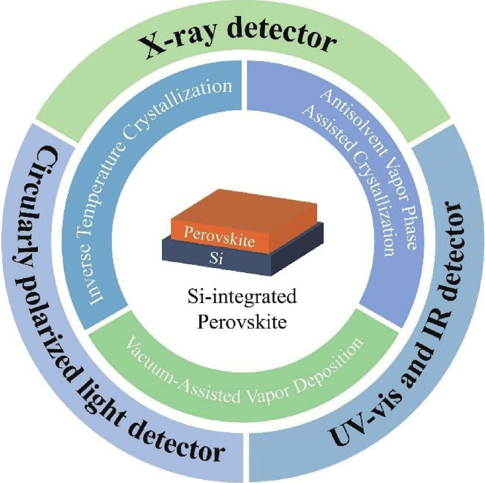
Fig. 1.
(Color online) Applications and integrated schemes of Si-integrated single crystal perovskite.
REVIEWS
Jing Weng1, 2, Molang Cai2, Xu Pan3 and Xing Li1,
Corresponding author: Xing Li, lixing2021@ime.ac.cn
Abstract: Metal halide perovskites (MHPs) have become promising optoelectronic materials due to their long carrier lifetimes and high mobility. However, the presence of defects and ion migration in MHPs results in high and unstable dark currents, which compromise the stability and detection performance of MHP-based optoelectronic devices. Interfacial engineering has proven to be an effective strategy to reduce defect density in MHPs and suppress ion migration. Given the compatibility of silicon (Si) and MHP processing technologies, coupled with the simplicity and cost-effectiveness of the approach, the integration of MHPs onto Si surfaces has become a prominent area of research. This integration not only enhances device performance but also expands their practical applications. This review provides an overview of the integration technologies for Si and single crystal MHPs, evaluates the advantages and limitations of various integration schemes (including inverse temperature crystallization, vacuum-assisted vapor deposition, and anti-solvent vapor-assisted crystallization), and explores the practical applications of Si/MHP-integrated optoelectronic devices with different structures. These optimized devices exhibit outstanding performance in X-ray detection, multi-wavelength photodetection, and circularly polarized light detection. This review provides a systematic reference for technological innovation and application expansion of Si/MHP-integrated devices.
Keywords: silicon, single crystal perovskite, heterogeneous integration, technology, application
| [1] |
Dou L T, Yang Y M, You J B, et al. Solution-processed hybrid perovskite photodetectors with high detectivity. Nat Commun, 2014, 5, 5404 doi: 10.1038/ncomms6404
|
| [2] |
Kim C O, Kim S, Shin D H, et al. High photoresponsivity in an all-graphene p-n vertical junction photodetector. Nat Commun, 2014, 5, 3249 doi: 10.1038/ncomms4249
|
| [3] |
Guan Y S, Qiao J, Liang Y Y, et al. A high mobility air-stable n-type organic small molecule semiconductor with high UV-visible-to-NIR photoresponse. Light Sci Appl, 2022, 11(1), 236 doi: 10.1038/s41377-022-00936-z
|
| [4] |
Tsarev S, Proniakova D, Liu X Q, et al. Vertically stacked monolithic perovskite colour photodetectors. Nature, 2025, 642(8068), 592 doi: 10.1038/s41586-025-09062-3
|
| [5] |
Wang K, Yang D, Wu C C, et al. Recent progress in fundamental understanding of halide perovskite semiconductors. Prog Mater Sci, 2019, 106, 100580 doi: 10.1016/j.pmatsci.2019.100580
|
| [6] |
Ebrahimkhani L, Nematollahi J, Mirkhani V, et al. Investigation of structural, electronic, and optical properties of halide perovskites with different amide cations: A first-principles approach. Mater Today Commun, 2024, 40, 110008 doi: 10.1016/j.mtcomm.2024.110008
|
| [7] |
Nketia-Yawson V, Nketia-Yawson B, Jo J W. Functional impact of gate dielectrics in emerging metal halide perovskite field-effect transistors. Mater Today Phys, 2024, 45, 101475 doi: 10.1016/j.mtphys.2024.101475
|
| [8] |
Zhang H C, Fu X, Tang Y, et al. Phase segregation due to ion migration in all-inorganic mixed-halide perovskite nanocrystals. Nat Commun, 2019, 10(1), 1088 doi: 10.1038/s41467-019-09047-7
|
| [9] |
Li Y H, Xie H B, Lim E L, et al. Recent progress of critical interface engineering for highly efficient and stable perovskite solar cells. Adv Energy Mater, 2022, 12, 2102730 doi: 10.1002/aenm.202102730
|
| [10] |
Jang C W, Shin D H, Choi S H. Performance enhancement of perovskite/porous-Si photodetectors by reducing the dark current with concomitant use of graphene quantum dots in the active layer and bathocuproine on the back surface. J Alloys Compd, 2023, 948, 169716 doi: 10.1016/j.jallcom.2023.169716
|
| [11] |
Zhao Y P, Yavuz I, Wang M H, et al. Suppressing ion migration in metal halide perovskite via interstitial doping with a trace amount of multivalent cations. Nat Mater, 2022, 21(12), 1396 doi: 10.1038/s41563-022-01390-3
|
| [12] |
Li R M, Peng J L, Xu Y L, et al. Pseudohalide additives enhanced perovskite photodetectors. Adv Opt Mater, 2021, 9(2), 2001587 doi: 10.1002/adom.202001587
|
| [13] |
Fang Y J, Dong Q F, Shao Y C, et al. Highly narrowband perovskite single-crystal photodetectors enabled by surface-charge recombination. Nat Photonics, 2015, 9, 679 doi: 10.1038/nphoton.2015.156
|
| [14] |
Liu X, Ren J, Chen Y A, et al. Recent progress in single crystal perovskite X-ray detectors. Sci China Inf Sci, 2024, 67(3), 131401 doi: 10.1007/s11432-023-3856-4
|
| [15] |
Mauthe S, Baumgartner Y, Sousa M, et al. High-speed III-V nanowire photodetector monolithically integrated on Si. Nat Commun, 2020, 11(1), 4565 doi: 10.1038/s41467-020-18374-z
|
| [16] |
Wei W, Zhang Y, Xu Q, et al. Monolithic integration of hybrid perovskite single crystals with heterogenous substrate for highly sensitive X-ray imaging. Nat Photonics, 2017, 11, 315 doi: 10.1038/nphoton.2017.43
|
| [17] |
Geng X S, Wang F W, Tian H, et al. Ultrafast photodetector by integrating perovskite directly on silicon wafer. ACS Nano, 2020, 14(3), 2860 doi: 10.1021/acsnano.9b06345
|
| [18] |
Zhang X Y, Weng W, Li L N, et al. Heterogeneous integration of chiral lead-chloride perovskite crystals with Si wafer for boosted circularly polarized light detection in solar-blind ultraviolet region. Small, 2021, 17(40), e2102884 doi: 10.1002/smll.202102884
|
| [19] |
Yang Z, Wang H, Guo L J, et al. A self-powered photodetector based on MAPbI3 single-crystal film/n-Si heterojunction with broadband response enhanced by pyro-phototronic and piezo-phototronic effects. Small, 2021, 17(32), e2101572 doi: 10.1002/smll.202101572
|
| [20] |
Zeng L H, Lin S H, Lou Z H, et al. Ultrafast and sensitive photodetector based on a PtSe2/silicon nanowire array heterojunction with a multiband spectral response from 200 to 1550 nm. NPG Asia Mater, 2018, 10, 352 doi: 10.1038/s41427-018-0035-4
|
| [21] |
Liu Z L, Xiong Z J, Yang S F, et al. Strained heterojunction enables high-performance, fully textured perovskite/silicon tandem solar cells. Joule, 2024, 8(10), 2834 doi: 10.1016/j.joule.2024.06.015
|
| [22] |
Zhou Y, Zhao L, Ni Z Y, et al. Heterojunction structures for reduced noise in large-area and sensitive perovskite X-ray detectors. Sci Adv, 2021, 7(36), eabg6716 doi: 10.1126/sciadv.abg6716
|
| [23] |
Qu W, Weng S K, Zhang L P, et al. Self-powered ultraviolet-visible-near infrared perovskite/silicon hybrid photodetectors based on a novel Si/SnO2/MAPbI3/MoO3 heterostructure. Appl Phys Express, 2020, 13(12), 121001 doi: 10.35848/1882-0786/abc5fa
|
| [24] |
Tian S K, Sui F, He K, et al. Co-axial silicon/perovskite heterojunction arrays for high-performance direct-conversion pixelated X-ray detectors. Nano Energy, 2020, 78, 105335 doi: 10.1016/j.nanoen.2020.105335
|
| [25] |
Li Z N, Huang S, Chen Y, et al. Vapor-deposited amino coupling of hybrid perovskite single crystals and silicon wafers toward highly efficient multiwavelength photodetection. ACS Appl Mater Interfaces, 2022, 14(46), 52476 doi: 10.1021/acsami.2c14466
|
| [26] |
Li Z N, Chen Y, Zhang C, et al. Phenyl-terminated coupling interface enabled highly efficient and stable multiwavelength perovskite single crystal/silicon integrated photodetector. ACS Appl Mater Interfaces, 2023, 15(13), 17377 doi: 10.1021/acsami.3c01008
|
| [27] |
Li J Y, Yang Y Z, Ye Z L, et al. Controlled high-quality perovskite single crystals growth for radiation detection: Nucleation and growth kinetics of antisolvent vapor-assisted crystallization. J Mater Sci Technol, 2025, 232, 276 doi: 10.1016/j.jmst.2025.02.019
|
| [28] |
Liu Y C, Zhang Y X, Yang Z, et al. Thinness- and shape-controlled growth for ultrathin single-crystalline perovskite wafers for mass production of superior photoelectronic devices. Adv Mater, 2016, 28(41), 9204 doi: 10.1002/adma.201601995
|
| [29] |
Liu D, Zheng Y C, Sui X Y, et al. Universal growth of perovskite thin monocrystals from high solute flux for sensitive self-driven X-ray detection. Nat Commun, 2024, 15(1), 2390 doi: 10.1038/s41467-024-46712-y
|
| [30] |
Wehrenfennig C, Liu M Z, Snaith H J, et al. Homogeneous emission line broadening in the organo lead halide perovskite CH3NH3PbI3–xClx. J Phys Chem Lett, 2014, 5(8), 1300 doi: 10.1021/jz500434p
|
| [31] |
Jiang J Z, Xiong M, Fan K, et al. Synergistic strain engineering of perovskite single crystals for highly stable and sensitive X-ray detectors with low-bias imaging and monitoring. Nat Photonics, 2022, 16, 575 doi: 10.1038/s41566-022-01024-9
|
| [32] |
Saidaminov M I, Adinolfi V, Comin R, et al. Planar-integrated single-crystalline perovskite photodetectors. Nat Commun, 2015, 6, 8724 doi: 10.1038/ncomms9724
|
| [33] |
Xu Z S, Han X, Wu W Q, et al. Controlled on-chip fabrication of large-scale perovskite single crystal arrays for high-performance laser and photodetector integration. Light Sci Appl, 2023, 12(1), 67 doi: 10.1038/s41377-023-01107-4
|
| [34] |
Yin W J, Shi T T, Yan Y F. Unusual defect physics in CH3NH3PbI3 perovskite solar cell absorber. Appl Phys Lett, 2014, 104(6), 063903 doi: 10.1063/1.4864778
|
| [35] |
Ke S M, Luo S Y, Gong J H, et al. Electric modulation of conduction in MAPbBr3 single crystals. J Adv Ceram, 2021, 10(2), 320 doi: 10.1007/s40145-020-0442-1
|
| [36] |
Chen C, Gao L, Gao W R, et al. Circularly polarized light detection using chiral hybrid perovskite. Nat Commun, 2019, 10(1), 1927 doi: 10.1038/s41467-019-09942-z
|
| [37] |
Kim M K, Choi Y S, Kim D, et al. Integration of large-area halide perovskite single crystals and substrates via chemical welding using an ionic liquid for applications in X-ray detection. ACS Appl Mater Interfaces, 2023, 15(49), 57404 doi: 10.1021/acsami.3c09854
|
| [38] |
Jiang X M, Xie S D, Xiao X, et al. Interface engineering of substrate-integrated single-crystal perovskite wafers for sensitive X-ray detection. Small Methods, 2024, 8(12), e2400099 doi: 10.1002/smtd.202400099
|
| [39] |
Chen J, Morrow D J, Fu Y P, et al. Single-crystal thin films of cesium lead bromide perovskite epitaxially grown on metal oxide perovskite (SrTiO3). J Am Chem Soc, 2017, 139(38), 13525 doi: 10.1021/jacs.7b07506
|
| [40] |
Yuan B L, Wei H M, Li J W, et al. Epitaxial Growth of quasi-intrinsic CsPbBr3 film on a SrTiO3 substrate by pulsed laser deposition. ACS Appl Electron Mater, 2021, 3(12), 5592 doi: 10.1021/acsaelm.1c01033
|
| [41] |
Li L Q, Tao L T, Wang L X, et al. Monolithic integration of perovskite heterojunction on TFT backplanes through vapor deposition for sensitive and stable X-ray imaging. Sci Adv, 2024, 10(17), eadj8659 doi: 10.1126/sciadv.adj8659
|
| [42] |
Liu Z Q, Wu H D, Yang H M, et al. Robust perovskite X-ray flat panel detector by anisotropic conductive adhesive to regulate thermal stress. ACS Energy Lett, 2024, 9(4), 1397 doi: 10.1021/acsenergylett.4c00195
|
| [43] |
Sakhatskyi K, Turedi B, Matt G J, et al. Stable perovskite single-crystal X-ray imaging detectors with single-photon sensitivity. Nat Photonics, 2023, 17, 510 doi: 10.1038/s41566-023-01207-y
|
| [44] |
Leung T L, Ahmad I, Syed A A, et al. Stability of 2D and quasi-2D perovskite materials and devices. Commun Mater, 2022, 3, 63 doi: 10.1038/s43246-022-00285-9
|
| [45] |
Zeng S H, Sui X Y, Liu D, et al. Molecular ordering in low-dimensional hybrid perovskites for improved X-ray detection. Angew Chem Int Ed, 2025, e202506973 doi: 10.1002/anie.202506973
|
| [46] |
Zheng X J, Zhao W, Wang P, et al. Ultrasensitive and stable X-ray detection using zero-dimensional lead-free perovskites. J Energy Chem, 2020, 49, 299 doi: 10.1016/j.jechem.2020.02.049
|
| [47] |
Jin P, Tang Y J, Li D W, et al. Realizing nearly-zero dark current and ultrahigh signal-to-noise ratio perovskite X-ray detector and image array by dark-current-shunting strategy. Nat Commun, 2023, 14(1), 626 doi: 10.1038/s41467-023-36313-6
|
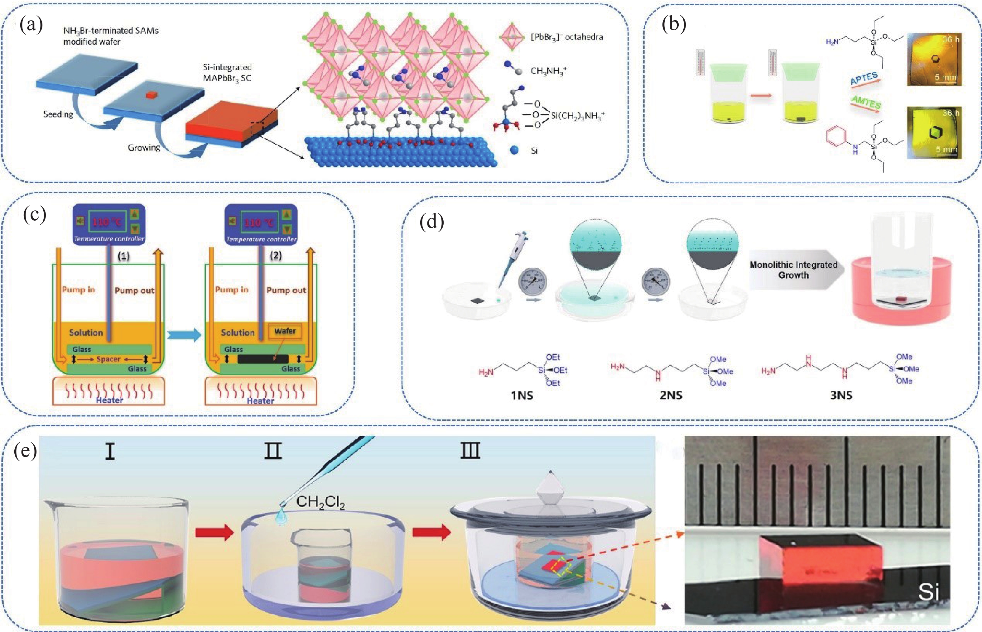
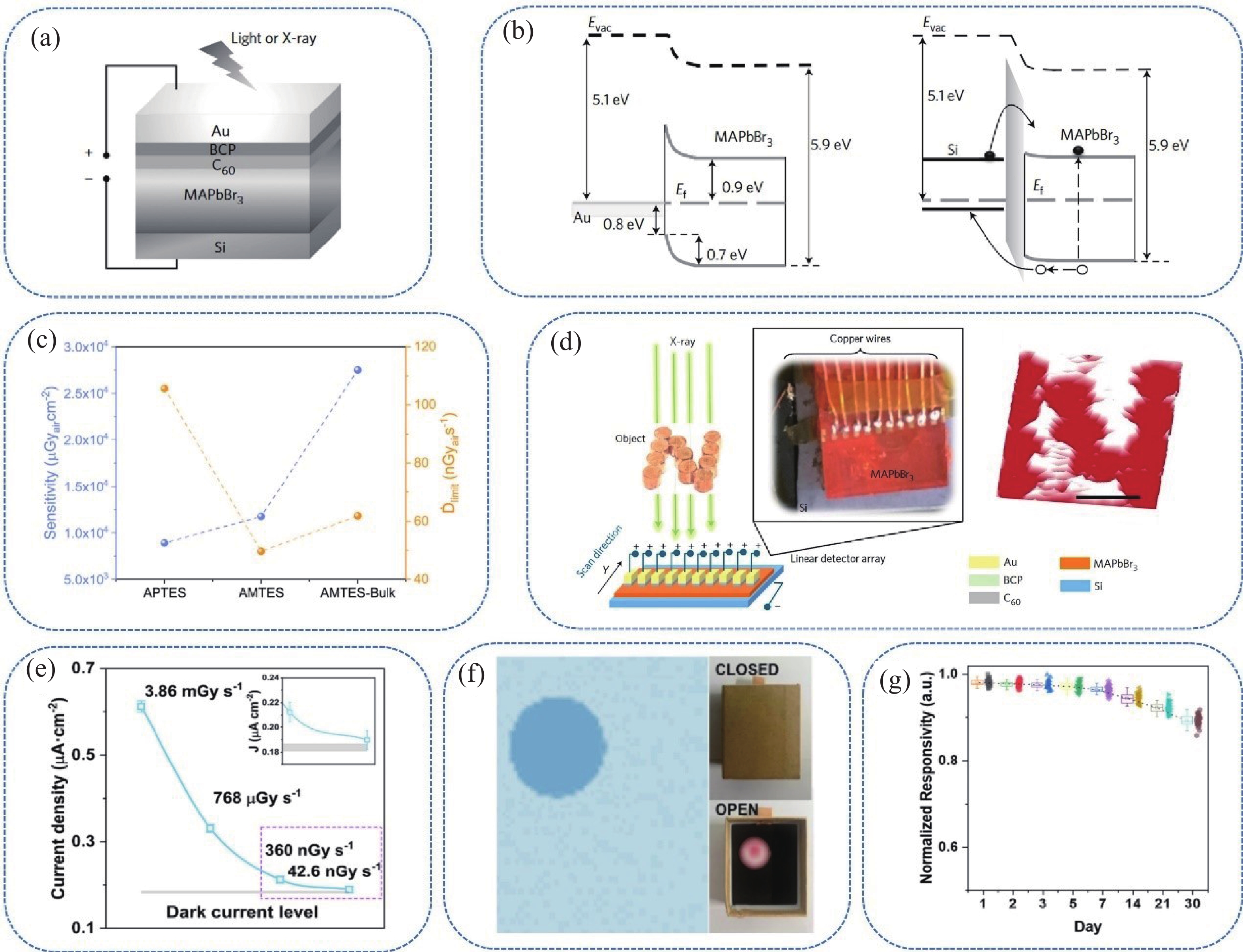
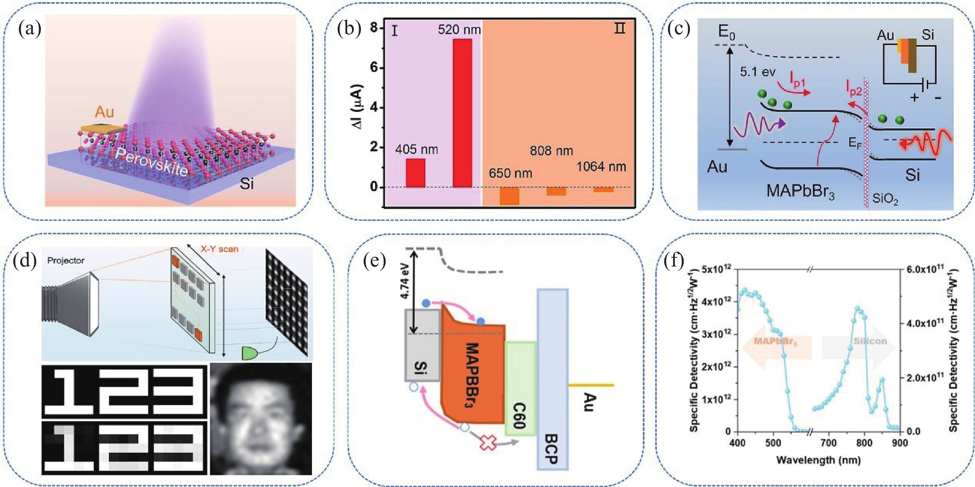
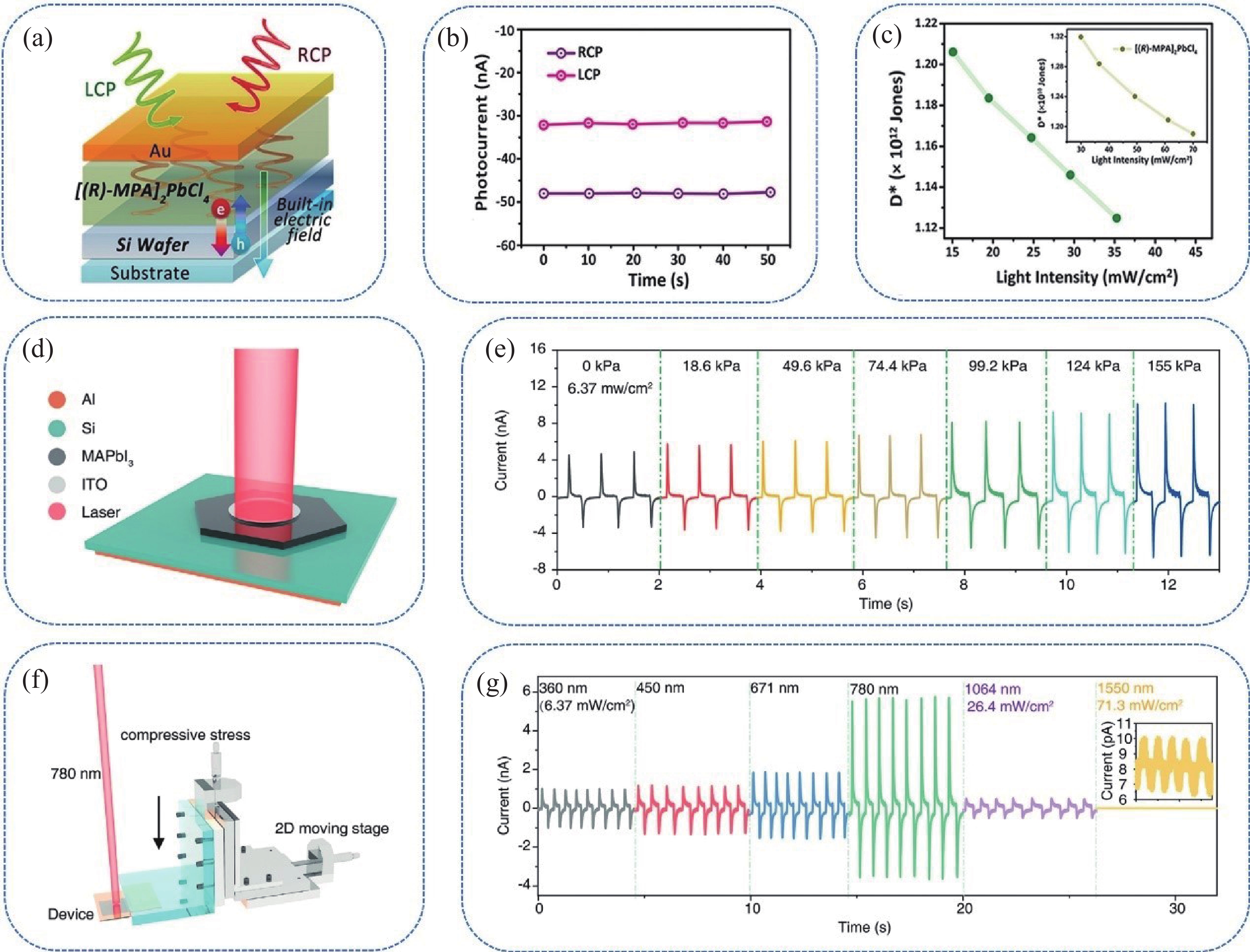
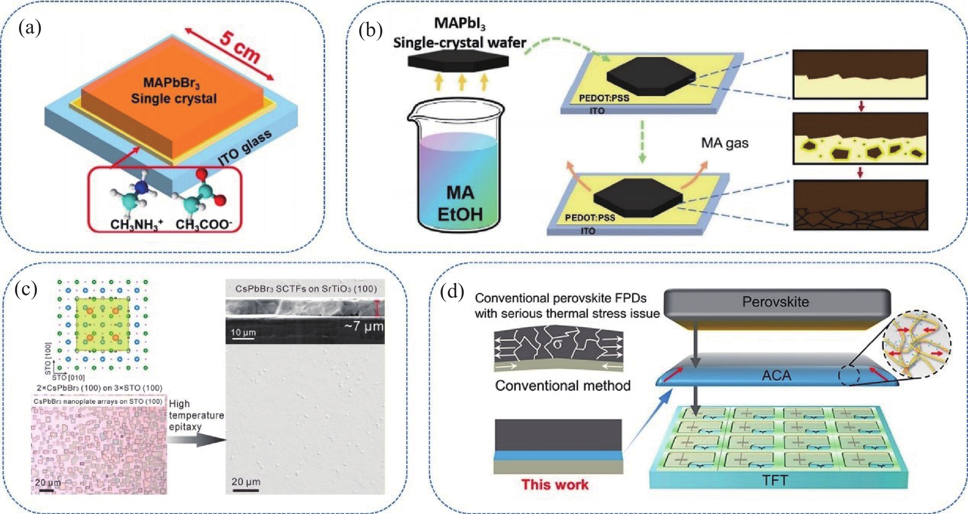
Table 1. Comparison of fabrication methods for MAPbBr3 crystals on silicon substrates.
| Method | Substrate modification | Seed crystal | Conditions of crystal growth | Crystal thickness (mm) | ||
| Solvent | Temperature | Time | ||||
| ITC[16] | Aminosiloxanes | Dimensions of ~300 μm | DMF | 70 °C | 6−8 h | 2−3 |
| VAVD[25, 26] | Aminosiloxanes | Appropriate size | DMF | 60 °C | 6−8 h | ~1.1 |
| AVC[17, 27] | / | / | Solvent: DMF Antisolvent: CH2Cl2 | Room temperature | Several days | 2−3 |
 DownLoad: CSV
| [1] |
Dou L T, Yang Y M, You J B, et al. Solution-processed hybrid perovskite photodetectors with high detectivity. Nat Commun, 2014, 5, 5404 doi: 10.1038/ncomms6404
|
| [2] |
Kim C O, Kim S, Shin D H, et al. High photoresponsivity in an all-graphene p-n vertical junction photodetector. Nat Commun, 2014, 5, 3249 doi: 10.1038/ncomms4249
|
| [3] |
Guan Y S, Qiao J, Liang Y Y, et al. A high mobility air-stable n-type organic small molecule semiconductor with high UV-visible-to-NIR photoresponse. Light Sci Appl, 2022, 11(1), 236 doi: 10.1038/s41377-022-00936-z
|
| [4] |
Tsarev S, Proniakova D, Liu X Q, et al. Vertically stacked monolithic perovskite colour photodetectors. Nature, 2025, 642(8068), 592 doi: 10.1038/s41586-025-09062-3
|
| [5] |
Wang K, Yang D, Wu C C, et al. Recent progress in fundamental understanding of halide perovskite semiconductors. Prog Mater Sci, 2019, 106, 100580 doi: 10.1016/j.pmatsci.2019.100580
|
| [6] |
Ebrahimkhani L, Nematollahi J, Mirkhani V, et al. Investigation of structural, electronic, and optical properties of halide perovskites with different amide cations: A first-principles approach. Mater Today Commun, 2024, 40, 110008 doi: 10.1016/j.mtcomm.2024.110008
|
| [7] |
Nketia-Yawson V, Nketia-Yawson B, Jo J W. Functional impact of gate dielectrics in emerging metal halide perovskite field-effect transistors. Mater Today Phys, 2024, 45, 101475 doi: 10.1016/j.mtphys.2024.101475
|
| [8] |
Zhang H C, Fu X, Tang Y, et al. Phase segregation due to ion migration in all-inorganic mixed-halide perovskite nanocrystals. Nat Commun, 2019, 10(1), 1088 doi: 10.1038/s41467-019-09047-7
|
| [9] |
Li Y H, Xie H B, Lim E L, et al. Recent progress of critical interface engineering for highly efficient and stable perovskite solar cells. Adv Energy Mater, 2022, 12, 2102730 doi: 10.1002/aenm.202102730
|
| [10] |
Jang C W, Shin D H, Choi S H. Performance enhancement of perovskite/porous-Si photodetectors by reducing the dark current with concomitant use of graphene quantum dots in the active layer and bathocuproine on the back surface. J Alloys Compd, 2023, 948, 169716 doi: 10.1016/j.jallcom.2023.169716
|
| [11] |
Zhao Y P, Yavuz I, Wang M H, et al. Suppressing ion migration in metal halide perovskite via interstitial doping with a trace amount of multivalent cations. Nat Mater, 2022, 21(12), 1396 doi: 10.1038/s41563-022-01390-3
|
| [12] |
Li R M, Peng J L, Xu Y L, et al. Pseudohalide additives enhanced perovskite photodetectors. Adv Opt Mater, 2021, 9(2), 2001587 doi: 10.1002/adom.202001587
|
| [13] |
Fang Y J, Dong Q F, Shao Y C, et al. Highly narrowband perovskite single-crystal photodetectors enabled by surface-charge recombination. Nat Photonics, 2015, 9, 679 doi: 10.1038/nphoton.2015.156
|
| [14] |
Liu X, Ren J, Chen Y A, et al. Recent progress in single crystal perovskite X-ray detectors. Sci China Inf Sci, 2024, 67(3), 131401 doi: 10.1007/s11432-023-3856-4
|
| [15] |
Mauthe S, Baumgartner Y, Sousa M, et al. High-speed III-V nanowire photodetector monolithically integrated on Si. Nat Commun, 2020, 11(1), 4565 doi: 10.1038/s41467-020-18374-z
|
| [16] |
Wei W, Zhang Y, Xu Q, et al. Monolithic integration of hybrid perovskite single crystals with heterogenous substrate for highly sensitive X-ray imaging. Nat Photonics, 2017, 11, 315 doi: 10.1038/nphoton.2017.43
|
| [17] |
Geng X S, Wang F W, Tian H, et al. Ultrafast photodetector by integrating perovskite directly on silicon wafer. ACS Nano, 2020, 14(3), 2860 doi: 10.1021/acsnano.9b06345
|
| [18] |
Zhang X Y, Weng W, Li L N, et al. Heterogeneous integration of chiral lead-chloride perovskite crystals with Si wafer for boosted circularly polarized light detection in solar-blind ultraviolet region. Small, 2021, 17(40), e2102884 doi: 10.1002/smll.202102884
|
| [19] |
Yang Z, Wang H, Guo L J, et al. A self-powered photodetector based on MAPbI3 single-crystal film/n-Si heterojunction with broadband response enhanced by pyro-phototronic and piezo-phototronic effects. Small, 2021, 17(32), e2101572 doi: 10.1002/smll.202101572
|
| [20] |
Zeng L H, Lin S H, Lou Z H, et al. Ultrafast and sensitive photodetector based on a PtSe2/silicon nanowire array heterojunction with a multiband spectral response from 200 to 1550 nm. NPG Asia Mater, 2018, 10, 352 doi: 10.1038/s41427-018-0035-4
|
| [21] |
Liu Z L, Xiong Z J, Yang S F, et al. Strained heterojunction enables high-performance, fully textured perovskite/silicon tandem solar cells. Joule, 2024, 8(10), 2834 doi: 10.1016/j.joule.2024.06.015
|
| [22] |
Zhou Y, Zhao L, Ni Z Y, et al. Heterojunction structures for reduced noise in large-area and sensitive perovskite X-ray detectors. Sci Adv, 2021, 7(36), eabg6716 doi: 10.1126/sciadv.abg6716
|
| [23] |
Qu W, Weng S K, Zhang L P, et al. Self-powered ultraviolet-visible-near infrared perovskite/silicon hybrid photodetectors based on a novel Si/SnO2/MAPbI3/MoO3 heterostructure. Appl Phys Express, 2020, 13(12), 121001 doi: 10.35848/1882-0786/abc5fa
|
| [24] |
Tian S K, Sui F, He K, et al. Co-axial silicon/perovskite heterojunction arrays for high-performance direct-conversion pixelated X-ray detectors. Nano Energy, 2020, 78, 105335 doi: 10.1016/j.nanoen.2020.105335
|
| [25] |
Li Z N, Huang S, Chen Y, et al. Vapor-deposited amino coupling of hybrid perovskite single crystals and silicon wafers toward highly efficient multiwavelength photodetection. ACS Appl Mater Interfaces, 2022, 14(46), 52476 doi: 10.1021/acsami.2c14466
|
| [26] |
Li Z N, Chen Y, Zhang C, et al. Phenyl-terminated coupling interface enabled highly efficient and stable multiwavelength perovskite single crystal/silicon integrated photodetector. ACS Appl Mater Interfaces, 2023, 15(13), 17377 doi: 10.1021/acsami.3c01008
|
| [27] |
Li J Y, Yang Y Z, Ye Z L, et al. Controlled high-quality perovskite single crystals growth for radiation detection: Nucleation and growth kinetics of antisolvent vapor-assisted crystallization. J Mater Sci Technol, 2025, 232, 276 doi: 10.1016/j.jmst.2025.02.019
|
| [28] |
Liu Y C, Zhang Y X, Yang Z, et al. Thinness- and shape-controlled growth for ultrathin single-crystalline perovskite wafers for mass production of superior photoelectronic devices. Adv Mater, 2016, 28(41), 9204 doi: 10.1002/adma.201601995
|
| [29] |
Liu D, Zheng Y C, Sui X Y, et al. Universal growth of perovskite thin monocrystals from high solute flux for sensitive self-driven X-ray detection. Nat Commun, 2024, 15(1), 2390 doi: 10.1038/s41467-024-46712-y
|
| [30] |
Wehrenfennig C, Liu M Z, Snaith H J, et al. Homogeneous emission line broadening in the organo lead halide perovskite CH3NH3PbI3–xClx. J Phys Chem Lett, 2014, 5(8), 1300 doi: 10.1021/jz500434p
|
| [31] |
Jiang J Z, Xiong M, Fan K, et al. Synergistic strain engineering of perovskite single crystals for highly stable and sensitive X-ray detectors with low-bias imaging and monitoring. Nat Photonics, 2022, 16, 575 doi: 10.1038/s41566-022-01024-9
|
| [32] |
Saidaminov M I, Adinolfi V, Comin R, et al. Planar-integrated single-crystalline perovskite photodetectors. Nat Commun, 2015, 6, 8724 doi: 10.1038/ncomms9724
|
| [33] |
Xu Z S, Han X, Wu W Q, et al. Controlled on-chip fabrication of large-scale perovskite single crystal arrays for high-performance laser and photodetector integration. Light Sci Appl, 2023, 12(1), 67 doi: 10.1038/s41377-023-01107-4
|
| [34] |
Yin W J, Shi T T, Yan Y F. Unusual defect physics in CH3NH3PbI3 perovskite solar cell absorber. Appl Phys Lett, 2014, 104(6), 063903 doi: 10.1063/1.4864778
|
| [35] |
Ke S M, Luo S Y, Gong J H, et al. Electric modulation of conduction in MAPbBr3 single crystals. J Adv Ceram, 2021, 10(2), 320 doi: 10.1007/s40145-020-0442-1
|
| [36] |
Chen C, Gao L, Gao W R, et al. Circularly polarized light detection using chiral hybrid perovskite. Nat Commun, 2019, 10(1), 1927 doi: 10.1038/s41467-019-09942-z
|
| [37] |
Kim M K, Choi Y S, Kim D, et al. Integration of large-area halide perovskite single crystals and substrates via chemical welding using an ionic liquid for applications in X-ray detection. ACS Appl Mater Interfaces, 2023, 15(49), 57404 doi: 10.1021/acsami.3c09854
|
| [38] |
Jiang X M, Xie S D, Xiao X, et al. Interface engineering of substrate-integrated single-crystal perovskite wafers for sensitive X-ray detection. Small Methods, 2024, 8(12), e2400099 doi: 10.1002/smtd.202400099
|
| [39] |
Chen J, Morrow D J, Fu Y P, et al. Single-crystal thin films of cesium lead bromide perovskite epitaxially grown on metal oxide perovskite (SrTiO3). J Am Chem Soc, 2017, 139(38), 13525 doi: 10.1021/jacs.7b07506
|
| [40] |
Yuan B L, Wei H M, Li J W, et al. Epitaxial Growth of quasi-intrinsic CsPbBr3 film on a SrTiO3 substrate by pulsed laser deposition. ACS Appl Electron Mater, 2021, 3(12), 5592 doi: 10.1021/acsaelm.1c01033
|
| [41] |
Li L Q, Tao L T, Wang L X, et al. Monolithic integration of perovskite heterojunction on TFT backplanes through vapor deposition for sensitive and stable X-ray imaging. Sci Adv, 2024, 10(17), eadj8659 doi: 10.1126/sciadv.adj8659
|
| [42] |
Liu Z Q, Wu H D, Yang H M, et al. Robust perovskite X-ray flat panel detector by anisotropic conductive adhesive to regulate thermal stress. ACS Energy Lett, 2024, 9(4), 1397 doi: 10.1021/acsenergylett.4c00195
|
| [43] |
Sakhatskyi K, Turedi B, Matt G J, et al. Stable perovskite single-crystal X-ray imaging detectors with single-photon sensitivity. Nat Photonics, 2023, 17, 510 doi: 10.1038/s41566-023-01207-y
|
| [44] |
Leung T L, Ahmad I, Syed A A, et al. Stability of 2D and quasi-2D perovskite materials and devices. Commun Mater, 2022, 3, 63 doi: 10.1038/s43246-022-00285-9
|
| [45] |
Zeng S H, Sui X Y, Liu D, et al. Molecular ordering in low-dimensional hybrid perovskites for improved X-ray detection. Angew Chem Int Ed, 2025, e202506973 doi: 10.1002/anie.202506973
|
| [46] |
Zheng X J, Zhao W, Wang P, et al. Ultrasensitive and stable X-ray detection using zero-dimensional lead-free perovskites. J Energy Chem, 2020, 49, 299 doi: 10.1016/j.jechem.2020.02.049
|
| [47] |
Jin P, Tang Y J, Li D W, et al. Realizing nearly-zero dark current and ultrahigh signal-to-noise ratio perovskite X-ray detector and image array by dark-current-shunting strategy. Nat Commun, 2023, 14(1), 626 doi: 10.1038/s41467-023-36313-6
|


Article views: 1912 Times PDF downloads: 463 Times Cited by: 0 Times
Received: 12 April 2025 Revised: 25 June 2025 Online: Accepted Manuscript: 15 July 2025Uncorrected proof: 23 July 2025Published: 15 December 2025
| Citation: |
Jing Weng, Molang Cai, Xu Pan, Xing Li. A minireview on technology and application of silicon integrated single crystal perovskite[J]. Journal of Semiconductors, 2025, 46(12): 121801. doi: 10.1088/1674-4926/25040012
****
J Weng, M L Cai, X Pan, and X Li, A minireview on technology and application of silicon integrated single crystal perovskite[J]. J. Semicond., 2025, 46(12), 121801 doi: 10.1088/1674-4926/25040012

|
 Jing Weng got her bachelor's degree from North China Electric Power University in 2025. Now she is a master student at Institute of Microelectronics of the Chinese Academy of Sciences. Her research focuses on the development of Si-integrated perovskite X-ray detectors
 Xing Li obtained his doctoral degree from East China University of Science and Technology in 2018 and then engaged in postdoctoral research at Beihang University. Since 2021, he has been with the Institute of Microelectronics of the Chinese Academy of Sciences as an associate professor. His current research interests include semiconductor radiation detectors and high-efficiency solar cells
| [1] |
Dou L T, Yang Y M, You J B, et al. Solution-processed hybrid perovskite photodetectors with high detectivity. Nat Commun, 2014, 5, 5404 doi: 10.1038/ncomms6404
|
| [2] |
Kim C O, Kim S, Shin D H, et al. High photoresponsivity in an all-graphene p-n vertical junction photodetector. Nat Commun, 2014, 5, 3249 doi: 10.1038/ncomms4249
|
| [3] |
Guan Y S, Qiao J, Liang Y Y, et al. A high mobility air-stable n-type organic small molecule semiconductor with high UV-visible-to-NIR photoresponse. Light Sci Appl, 2022, 11(1), 236 doi: 10.1038/s41377-022-00936-z
|
| [4] |
Tsarev S, Proniakova D, Liu X Q, et al. Vertically stacked monolithic perovskite colour photodetectors. Nature, 2025, 642(8068), 592 doi: 10.1038/s41586-025-09062-3
|
| [5] |
Wang K, Yang D, Wu C C, et al. Recent progress in fundamental understanding of halide perovskite semiconductors. Prog Mater Sci, 2019, 106, 100580 doi: 10.1016/j.pmatsci.2019.100580
|
| [6] |
Ebrahimkhani L, Nematollahi J, Mirkhani V, et al. Investigation of structural, electronic, and optical properties of halide perovskites with different amide cations: A first-principles approach. Mater Today Commun, 2024, 40, 110008 doi: 10.1016/j.mtcomm.2024.110008
|
| [7] |
Nketia-Yawson V, Nketia-Yawson B, Jo J W. Functional impact of gate dielectrics in emerging metal halide perovskite field-effect transistors. Mater Today Phys, 2024, 45, 101475 doi: 10.1016/j.mtphys.2024.101475
|
| [8] |
Zhang H C, Fu X, Tang Y, et al. Phase segregation due to ion migration in all-inorganic mixed-halide perovskite nanocrystals. Nat Commun, 2019, 10(1), 1088 doi: 10.1038/s41467-019-09047-7
|
| [9] |
Li Y H, Xie H B, Lim E L, et al. Recent progress of critical interface engineering for highly efficient and stable perovskite solar cells. Adv Energy Mater, 2022, 12, 2102730 doi: 10.1002/aenm.202102730
|
| [10] |
Jang C W, Shin D H, Choi S H. Performance enhancement of perovskite/porous-Si photodetectors by reducing the dark current with concomitant use of graphene quantum dots in the active layer and bathocuproine on the back surface. J Alloys Compd, 2023, 948, 169716 doi: 10.1016/j.jallcom.2023.169716
|
| [11] |
Zhao Y P, Yavuz I, Wang M H, et al. Suppressing ion migration in metal halide perovskite via interstitial doping with a trace amount of multivalent cations. Nat Mater, 2022, 21(12), 1396 doi: 10.1038/s41563-022-01390-3
|
| [12] |
Li R M, Peng J L, Xu Y L, et al. Pseudohalide additives enhanced perovskite photodetectors. Adv Opt Mater, 2021, 9(2), 2001587 doi: 10.1002/adom.202001587
|
| [13] |
Fang Y J, Dong Q F, Shao Y C, et al. Highly narrowband perovskite single-crystal photodetectors enabled by surface-charge recombination. Nat Photonics, 2015, 9, 679 doi: 10.1038/nphoton.2015.156
|
| [14] |
Liu X, Ren J, Chen Y A, et al. Recent progress in single crystal perovskite X-ray detectors. Sci China Inf Sci, 2024, 67(3), 131401 doi: 10.1007/s11432-023-3856-4
|
| [15] |
Mauthe S, Baumgartner Y, Sousa M, et al. High-speed III-V nanowire photodetector monolithically integrated on Si. Nat Commun, 2020, 11(1), 4565 doi: 10.1038/s41467-020-18374-z
|
| [16] |
Wei W, Zhang Y, Xu Q, et al. Monolithic integration of hybrid perovskite single crystals with heterogenous substrate for highly sensitive X-ray imaging. Nat Photonics, 2017, 11, 315 doi: 10.1038/nphoton.2017.43
|
| [17] |
Geng X S, Wang F W, Tian H, et al. Ultrafast photodetector by integrating perovskite directly on silicon wafer. ACS Nano, 2020, 14(3), 2860 doi: 10.1021/acsnano.9b06345
|
| [18] |
Zhang X Y, Weng W, Li L N, et al. Heterogeneous integration of chiral lead-chloride perovskite crystals with Si wafer for boosted circularly polarized light detection in solar-blind ultraviolet region. Small, 2021, 17(40), e2102884 doi: 10.1002/smll.202102884
|
| [19] |
Yang Z, Wang H, Guo L J, et al. A self-powered photodetector based on MAPbI3 single-crystal film/n-Si heterojunction with broadband response enhanced by pyro-phototronic and piezo-phototronic effects. Small, 2021, 17(32), e2101572 doi: 10.1002/smll.202101572
|
| [20] |
Zeng L H, Lin S H, Lou Z H, et al. Ultrafast and sensitive photodetector based on a PtSe2/silicon nanowire array heterojunction with a multiband spectral response from 200 to 1550 nm. NPG Asia Mater, 2018, 10, 352 doi: 10.1038/s41427-018-0035-4
|
| [21] |
Liu Z L, Xiong Z J, Yang S F, et al. Strained heterojunction enables high-performance, fully textured perovskite/silicon tandem solar cells. Joule, 2024, 8(10), 2834 doi: 10.1016/j.joule.2024.06.015
|
| [22] |
Zhou Y, Zhao L, Ni Z Y, et al. Heterojunction structures for reduced noise in large-area and sensitive perovskite X-ray detectors. Sci Adv, 2021, 7(36), eabg6716 doi: 10.1126/sciadv.abg6716
|
| [23] |
Qu W, Weng S K, Zhang L P, et al. Self-powered ultraviolet-visible-near infrared perovskite/silicon hybrid photodetectors based on a novel Si/SnO2/MAPbI3/MoO3 heterostructure. Appl Phys Express, 2020, 13(12), 121001 doi: 10.35848/1882-0786/abc5fa
|
| [24] |
Tian S K, Sui F, He K, et al. Co-axial silicon/perovskite heterojunction arrays for high-performance direct-conversion pixelated X-ray detectors. Nano Energy, 2020, 78, 105335 doi: 10.1016/j.nanoen.2020.105335
|
| [25] |
Li Z N, Huang S, Chen Y, et al. Vapor-deposited amino coupling of hybrid perovskite single crystals and silicon wafers toward highly efficient multiwavelength photodetection. ACS Appl Mater Interfaces, 2022, 14(46), 52476 doi: 10.1021/acsami.2c14466
|
| [26] |
Li Z N, Chen Y, Zhang C, et al. Phenyl-terminated coupling interface enabled highly efficient and stable multiwavelength perovskite single crystal/silicon integrated photodetector. ACS Appl Mater Interfaces, 2023, 15(13), 17377 doi: 10.1021/acsami.3c01008
|
| [27] |
Li J Y, Yang Y Z, Ye Z L, et al. Controlled high-quality perovskite single crystals growth for radiation detection: Nucleation and growth kinetics of antisolvent vapor-assisted crystallization. J Mater Sci Technol, 2025, 232, 276 doi: 10.1016/j.jmst.2025.02.019
|
| [28] |
Liu Y C, Zhang Y X, Yang Z, et al. Thinness- and shape-controlled growth for ultrathin single-crystalline perovskite wafers for mass production of superior photoelectronic devices. Adv Mater, 2016, 28(41), 9204 doi: 10.1002/adma.201601995
|
| [29] |
Liu D, Zheng Y C, Sui X Y, et al. Universal growth of perovskite thin monocrystals from high solute flux for sensitive self-driven X-ray detection. Nat Commun, 2024, 15(1), 2390 doi: 10.1038/s41467-024-46712-y
|
| [30] |
Wehrenfennig C, Liu M Z, Snaith H J, et al. Homogeneous emission line broadening in the organo lead halide perovskite CH3NH3PbI3–xClx. J Phys Chem Lett, 2014, 5(8), 1300 doi: 10.1021/jz500434p
|
| [31] |
Jiang J Z, Xiong M, Fan K, et al. Synergistic strain engineering of perovskite single crystals for highly stable and sensitive X-ray detectors with low-bias imaging and monitoring. Nat Photonics, 2022, 16, 575 doi: 10.1038/s41566-022-01024-9
|
| [32] |
Saidaminov M I, Adinolfi V, Comin R, et al. Planar-integrated single-crystalline perovskite photodetectors. Nat Commun, 2015, 6, 8724 doi: 10.1038/ncomms9724
|
| [33] |
Xu Z S, Han X, Wu W Q, et al. Controlled on-chip fabrication of large-scale perovskite single crystal arrays for high-performance laser and photodetector integration. Light Sci Appl, 2023, 12(1), 67 doi: 10.1038/s41377-023-01107-4
|
| [34] |
Yin W J, Shi T T, Yan Y F. Unusual defect physics in CH3NH3PbI3 perovskite solar cell absorber. Appl Phys Lett, 2014, 104(6), 063903 doi: 10.1063/1.4864778
|
| [35] |
Ke S M, Luo S Y, Gong J H, et al. Electric modulation of conduction in MAPbBr3 single crystals. J Adv Ceram, 2021, 10(2), 320 doi: 10.1007/s40145-020-0442-1
|
| [36] |
Chen C, Gao L, Gao W R, et al. Circularly polarized light detection using chiral hybrid perovskite. Nat Commun, 2019, 10(1), 1927 doi: 10.1038/s41467-019-09942-z
|
| [37] |
Kim M K, Choi Y S, Kim D, et al. Integration of large-area halide perovskite single crystals and substrates via chemical welding using an ionic liquid for applications in X-ray detection. ACS Appl Mater Interfaces, 2023, 15(49), 57404 doi: 10.1021/acsami.3c09854
|
| [38] |
Jiang X M, Xie S D, Xiao X, et al. Interface engineering of substrate-integrated single-crystal perovskite wafers for sensitive X-ray detection. Small Methods, 2024, 8(12), e2400099 doi: 10.1002/smtd.202400099
|
| [39] |
Chen J, Morrow D J, Fu Y P, et al. Single-crystal thin films of cesium lead bromide perovskite epitaxially grown on metal oxide perovskite (SrTiO3). J Am Chem Soc, 2017, 139(38), 13525 doi: 10.1021/jacs.7b07506
|
| [40] |
Yuan B L, Wei H M, Li J W, et al. Epitaxial Growth of quasi-intrinsic CsPbBr3 film on a SrTiO3 substrate by pulsed laser deposition. ACS Appl Electron Mater, 2021, 3(12), 5592 doi: 10.1021/acsaelm.1c01033
|
| [41] |
Li L Q, Tao L T, Wang L X, et al. Monolithic integration of perovskite heterojunction on TFT backplanes through vapor deposition for sensitive and stable X-ray imaging. Sci Adv, 2024, 10(17), eadj8659 doi: 10.1126/sciadv.adj8659
|
| [42] |
Liu Z Q, Wu H D, Yang H M, et al. Robust perovskite X-ray flat panel detector by anisotropic conductive adhesive to regulate thermal stress. ACS Energy Lett, 2024, 9(4), 1397 doi: 10.1021/acsenergylett.4c00195
|
| [43] |
Sakhatskyi K, Turedi B, Matt G J, et al. Stable perovskite single-crystal X-ray imaging detectors with single-photon sensitivity. Nat Photonics, 2023, 17, 510 doi: 10.1038/s41566-023-01207-y
|
| [44] |
Leung T L, Ahmad I, Syed A A, et al. Stability of 2D and quasi-2D perovskite materials and devices. Commun Mater, 2022, 3, 63 doi: 10.1038/s43246-022-00285-9
|
| [45] |
Zeng S H, Sui X Y, Liu D, et al. Molecular ordering in low-dimensional hybrid perovskites for improved X-ray detection. Angew Chem Int Ed, 2025, e202506973 doi: 10.1002/anie.202506973
|
| [46] |
Zheng X J, Zhao W, Wang P, et al. Ultrasensitive and stable X-ray detection using zero-dimensional lead-free perovskites. J Energy Chem, 2020, 49, 299 doi: 10.1016/j.jechem.2020.02.049
|
| [47] |
Jin P, Tang Y J, Li D W, et al. Realizing nearly-zero dark current and ultrahigh signal-to-noise ratio perovskite X-ray detector and image array by dark-current-shunting strategy. Nat Commun, 2023, 14(1), 626 doi: 10.1038/s41467-023-36313-6
|

 WeChat ID
Journal of Semiconductors © 2017 All Rights Reserved 京ICP备05085259号-2


