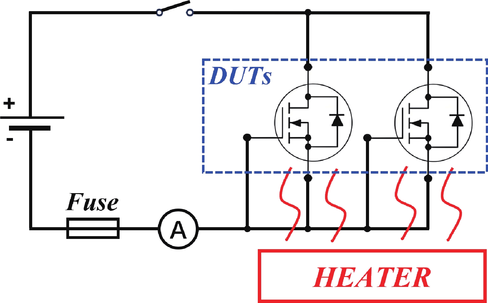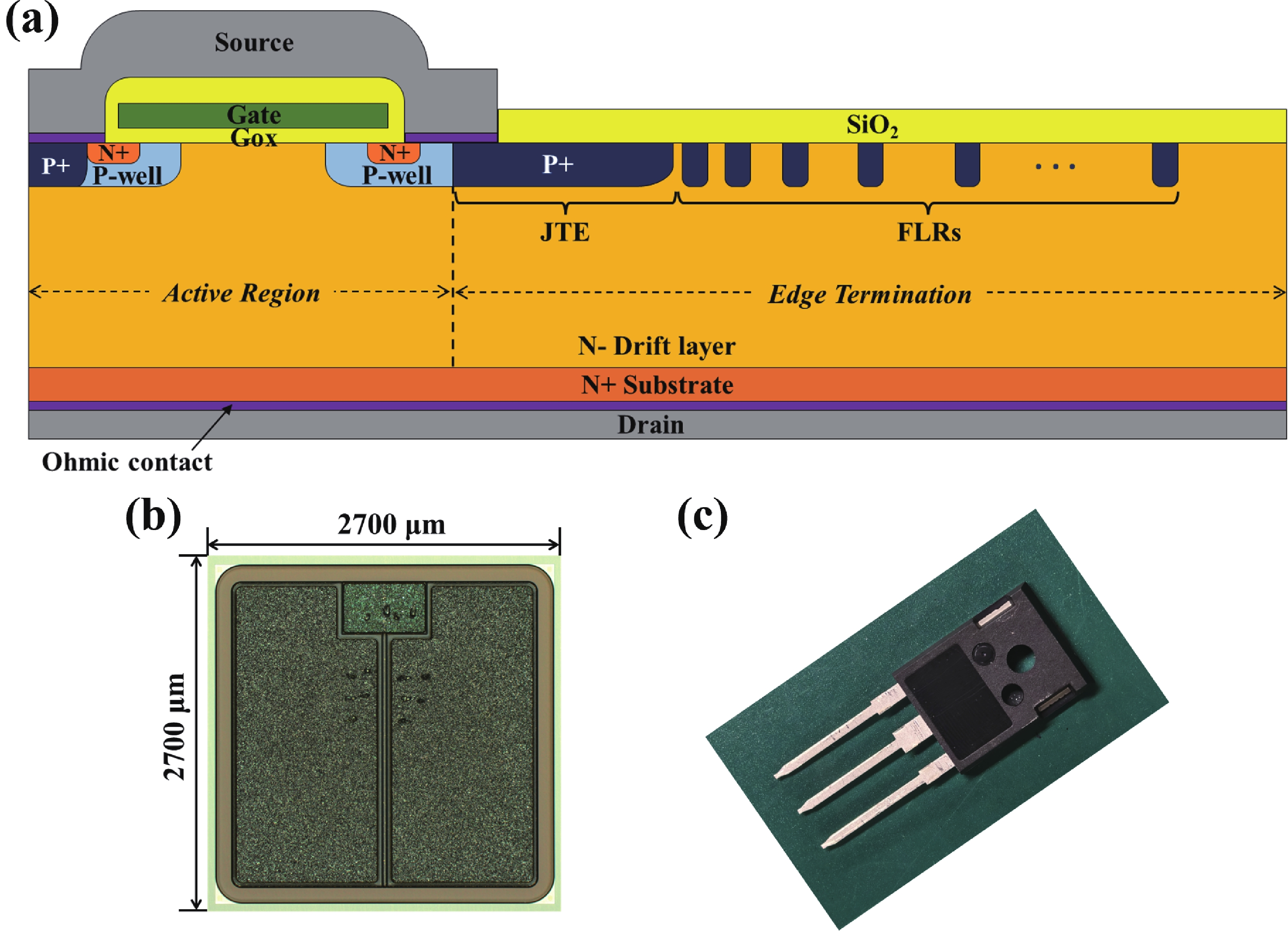
Fig. 1.
(Color online) (a) Typical schematic of SiC MOSFET. (b) Appearance of a chip. (c) A device in TO247 package.
ARTICLES
Fanpeng Zeng1, Yingxin Cui1, , Zhixin Liu1, Zicheng Lu1, Lingling Lai1, Shoulai Gong1, Haochen Wang2, Peng Dong2, and Jisheng Han1
Corresponding author: Yingxin Cui, cuiyingxin@sdu.edu.cn; Peng Dong, dongpeng0711@foxmail.com
Abstract: High-temperature reverse bias (HTRB) is one of the most critical reliability for SiC MOSFET, and the termination region is widely regarded as the sensitive area under HTRB stress. Interestingly, through systematically monitoring of the degradation behavior of static electrical parameters under different voltage, this study reveals that the elevated reverse bias (ERB) stress can also induce damage in the gate oxide, which results in the hole trapping and a negative shift of the threshold voltage. Deep level transient spectroscopy (DLTS) measurements were performed and showed that the interface trap density in the gate oxide is promoted after ERB stress. Surprisingly, the reverse leakage current after ERB stress is significantly deteriorated at a gate bias of 0 V, while effectively suppressed by applying a negative gate bias (−5 V), which point to the synergistic effects of channel region on the breakdown voltage. Based on the gate oxide degradations and TCAD simulations, it is elucidated that the trapped positive interface charges in gate oxide cause band bending, leading to the formation of an electron accumulation layer in the channel region at 0 V gate bias and thus resulting in a dominant leakage path. This work reveals the impact and mechanism of the ERB stress induced gate oxide damage on the breakdown voltage and highlights the importance of gate oxide protection, which is of great significance for improving the reliability of SiC MOSFETs in elevated voltage applications.
Keywords: elevated reverse bias stress, gate oxide degradation, synergistic effect, interface traps, SiC MOSFET
| [1] |
She X, Huang A Q, Lucia O, et al. Review of silicon carbide power devices and their applications. IEEE Trans Ind Electron, 2017, 64(10): 8193 doi: 10.1109/TIE.2017.2652401
|
| [2] |
Saito W. A future outlook of power devices from the viewpoint of power electronics trends. IEEE Trans Electron Devices, 2024, 71(3): 1356 doi: 10.1109/TED.2023.3332611
|
| [3] |
Hazra S, De A K, Cheng L, et al. High switching performance of 1700V, 50A SiC power MOSFET over Si IGBT/BiMOSFET for advanced power conversion applications. IEEE Trans Power Electron, 2016, 31(7): 4742 doi: 10.1109/TPEL.2015.2432012
|
| [4] |
Kumar A, Moradpour M, Losito M, et al. Wide band gap devices and their application in power electronics. Energies, 2022, 15(23): 9172 doi: 10.3390/en15239172
|
| [5] |
Millán J, Godignon P, Perpiñà X, et al. A survey of wide bandgap power semiconductor devices. IEEE Trans Power Electron, 2014, 29(5): 2155 doi: 10.1109/TPEL.2013.2268900
|
| [6] |
Wang H, Blaabjerg F. Power electronics reliability: State of the art and outlook. IEEE J Emerg Sel Topics Power Electron, 2021, 9(6): 6476 doi: 10.1109/JESTPE.2020.3037161
|
| [7] |
Lutz J, Schlangenotto H, Scheuermann U, et al. Semiconductor power devices: Physics, characteristics, reliability. Springer, 2011 doi: 10.1007/978-3-319-70917-8
|
| [8] |
Jayant Baliga B. Silicon carbide power devices. World Scientific, 2006 doi: 10.1109/smicnd.1998.732305
|
| [9] |
Yuan X B, Laird I, Walder S. Opportunities, challenges, and potential solutions in the application of fast-switching SiC power devices and converters. IEEE Trans Power Electron, 2021, 36(4): 3925 doi: 10.1109/TPEL.2020.3024862
|
| [10] |
Du Y J, Li J Y, Wang P, et al. Comparison of high voltage SiC MOSFET and Si IGBT power module thermal performance. Mater Sci Forum, 2019, 954: 194 doi: 10.4028/www.scientific.net/MSF.954.194
|
| [11] |
Rahimo M. Performance evaluation and expected challenges of silicon carbide power MOSFETs for high voltage applications. Mater Sci Forum, 2017, 897: 649 doi: 10.4028/www.scientific.net/MSF.897.649
|
| [12] |
Wei J X, Wei Z X, Fu H, et al. Review on the reliability mechanisms of SiC power MOSFETs: A comparison between planar-gate and trench-gate structures. IEEE Trans Power Electron, 2023, 38(7): 8990 doi: 10.1109/TPEL.2023.3265864
|
| [13] |
Salmen P, Friedrichs P. Qualifying a silicon carbide power module: Reliability testing beyond the standards of silicon devices. CIPS 2022; 12th International Conference on Integrated Power Electronics Systems, 2022: 1 doi: https://www.vde-verlag.de/proceedings-de/455757077.html
|
| [14] |
Moultif N, Joubert E, Masmoudi M, et al. Characterization of HTRB stress effects on SiC MOSFETs using photon emission spectral signatures. Microelectron Reliab, 2017, 76: 243 doi: 10.1016/j.microrel.2017.07.013
|
| [15] |
Tang J Y, Duan Y H, Liu P. Investigation of degradation and failure mechanism in 1200 V planar SiC MOSFET under statical accelerated lifetime Test. IEEE Trans Device Mater Relib, 2025, 25(3): 441 doi: 10.1109/TDMR.2025.3577612
|
| [16] |
Matsushima H, Yamada R, Shima A. Two mechanisms of charge accumulation in edge termination of 4H-SiC diodes caused by high-temperature bias stress and high-temperature and high-humidity bias stress. IEEE Trans Electron Devices, 2018, 65(8): 3318 doi: 10.1109/TED.2018.2845376
|
| [17] |
Dong P, Li P, Zhang L, et al. Atomistic mechanism of 4H-SiC/SiO2 interface carrier-trapping effects on breakdown-voltage degradation in power devices. Phys Rev Appl, 2021, 15(3): 034007 doi: 10.1103/PhysRevApplied.15.034007
|
| [18] |
Yu M Y, Shen Y, Ma H P, et al. Experiment and analysis of termination robustness design for 1200 V 4H-SiC MOSFET. Nanomaterials, 2025, 15(11): 805 doi: 10.3390/nano15110805
|
| [19] |
Fiorenza P, Alessandrino M S, Carbone B, et al. Understanding the role of threading dislocations on 4H-SiC MOSFET breakdown under high temperature reverse bias stress. Nanotechnology, 2020, 31(12): 125203 doi: 10.1088/1361-6528/ab5ff6
|
| [20] |
Fiorenza P, Adamo S, Alessandrino M S, et al. Correlation between MOSFETs breakdown and 4H-SiC epitaxial defects. 2021 IEEE International Reliability Physics Symposium (IRPS), 2021: 1 doi: 10.1109/irps46558.2021.9405148
|
| [21] |
Senzaki J, Kojima K, Kato T, et al. Correlation between reliability of thermal oxides and dislocations in n-type 4H-SiC epitaxial wafers. Appl Phys Lett, 2006, 89(2): 022909 doi: 10.1063/1.2221525
|
| [22] |
Jouha W, Masmoudi M, El Oualkadi A, et al. Physical study of SiC power MOSFETs towards HTRB stress based on C-V characteristics. IEEE Trans Device Mater Relib, 2020, 20(3): 506 doi: 10.1109/TDMR.2020.2999029
|
| [23] |
Ren M, Liang S Q, Zhou T, et al. Gate oxide failure mechanisms of SiC MOSFET related to electro-thermomechanical stress under HTRB and HTGB test. 2024 36th International Symposium on Power Semiconductor Devices and ICs (ISPSD), 2024: 208 doi: 10.1109/ispsd59661.2024.10579620
|
| [24] |
Garete A J, Li Z W, Fung Y W, et al. Reliability performance study of molding compounds on high voltage molded leaded package. 2023 18th International Microsystems, Packaging, Assembly and Circuits Technology Conference (IMPACT), 2023: 67 doi: 10.1109/impact59481.2023.10348634
|
| [25] |
Ooi A L, Goh D, Ngwan V C. High temperature reverse bias (HTRB) & temperature humidity bias (THB) reliability failure mechanisms and improvements in trench power MOSFET and IGBT. IEEE J Electron Devices Soc, 2021, 9: 1181 doi: 10.1109/JEDS.2021.3109347
|
| [26] |
Potera R R, Witt T, Zheng Y. Analysis of transient HTRB leakage in a SiC field ring termination. 2020 IEEE International Reliability Physics Symposium (IRPS), 2020: 1 doi: 10.1109/IRPS45951.2020.9129571
|
| [27] |
Aichinger T, Rescher G, Pobegen G. Threshold voltage peculiarities and bias temperature instabilities of SiC MOSFETs. Microelectron Reliab, 2018, 80: 68 doi: 10.1016/j.microrel.2017.11.020
|
| [28] |
JEDEC Solid State Technology Association. JEP-183A: Guidelines for Measuring the Reliability of Solid-State Drives (SSDs). JEDEC Standard, 2023 doi: https://www.jedec.org/
|
| [29] |
Cai J H, Peng Y J, Fan J F, et al. The reverse bias reliability of SiC MOSFET under different conditions and failure analysis. 2024 25th International Conference on Electronic Packaging Technology (ICEPT), 2024: 1 doi: 10.1109/icept63120.2024.10668576
|
| [30] |
Chowdhury S, Matocha K, Powell B, et al. Next generation 1200V, 3.5mΩ∙cm2 SiC planar gate MOSFET with excellent HTRB reliability. 2018 IEEE 30th International Symposium on Power Semiconductor Devices and ICs (ISPSD), 2018: 427 doi: 10.1109/ISPSD.2018.8393694
|
| [31] |
Rudenko T E, Osiyuk I N, Tyagulski I P, et al. Interface trap properties of thermally oxidized n-type 4H–SiC and 6H–SiC. Solid State Electron, 2005, 49(4): 545 doi: 10.1016/j.sse.2004.12.006
|
| [32] |
Jiang S, Zhang M, Meng X W, et al. Trap characterization of trench-gate SiC MOSFETs based on transient drain current. IEEE Trans Power Electron, 2023, 38(5): 6555 doi: 10.1109/TPEL.2023.3242950
|
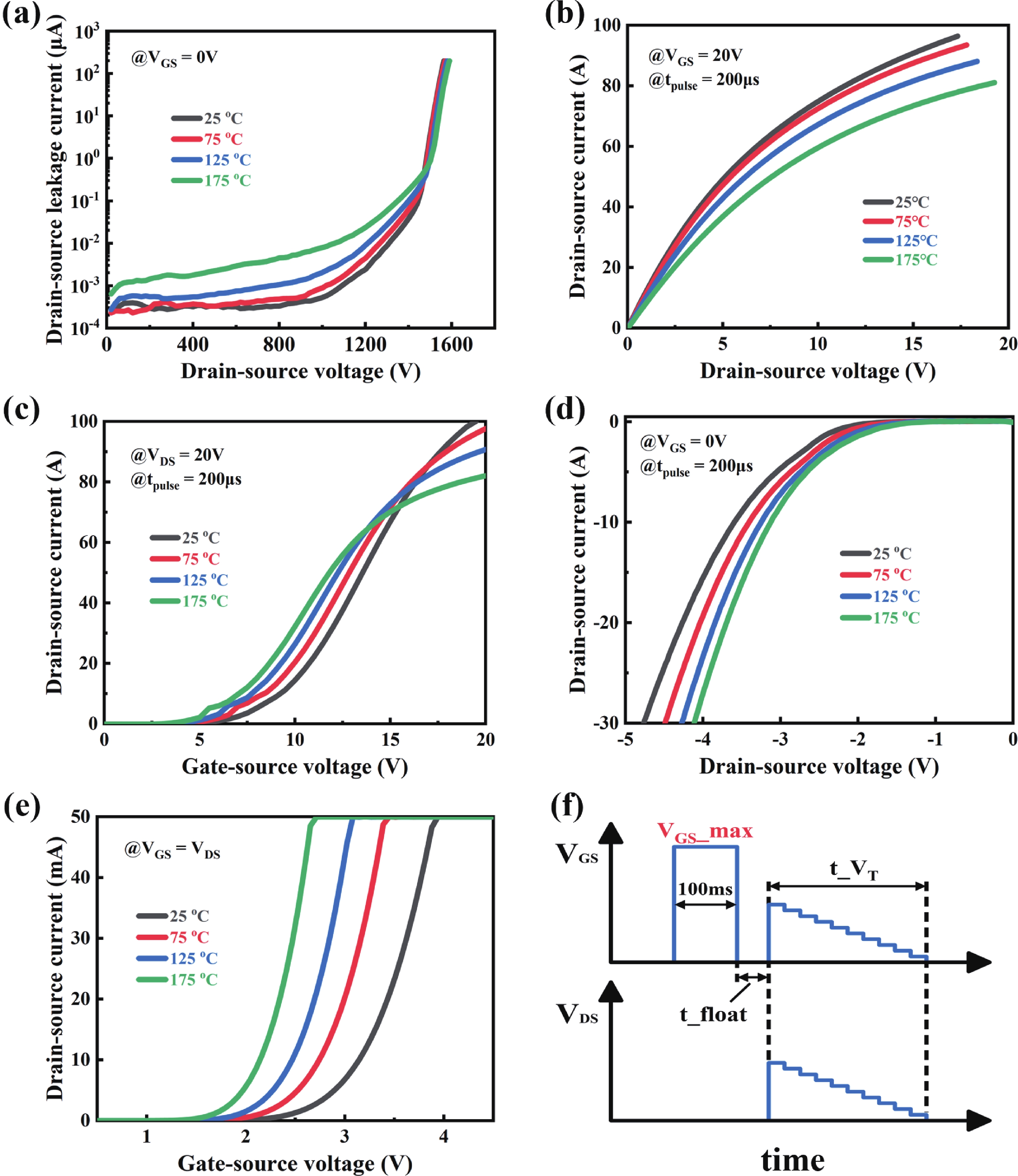
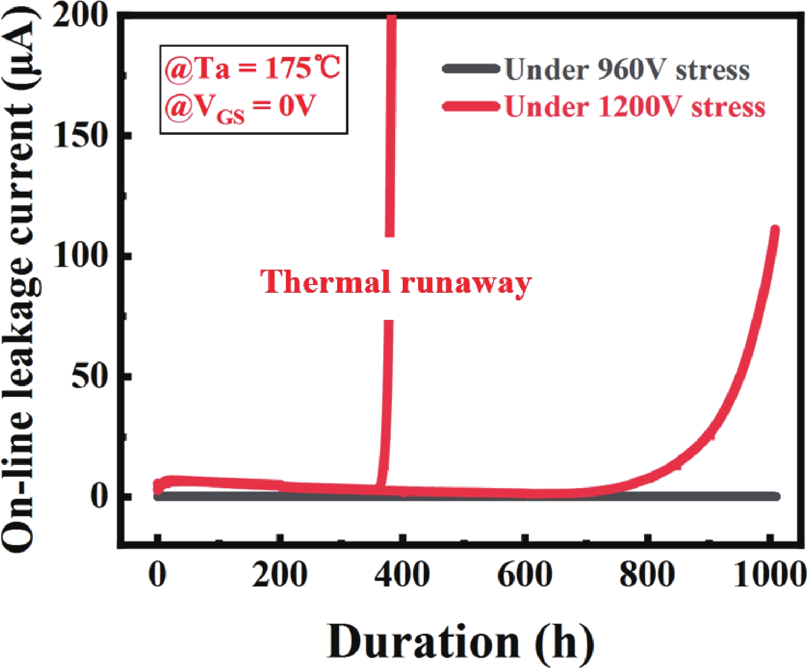
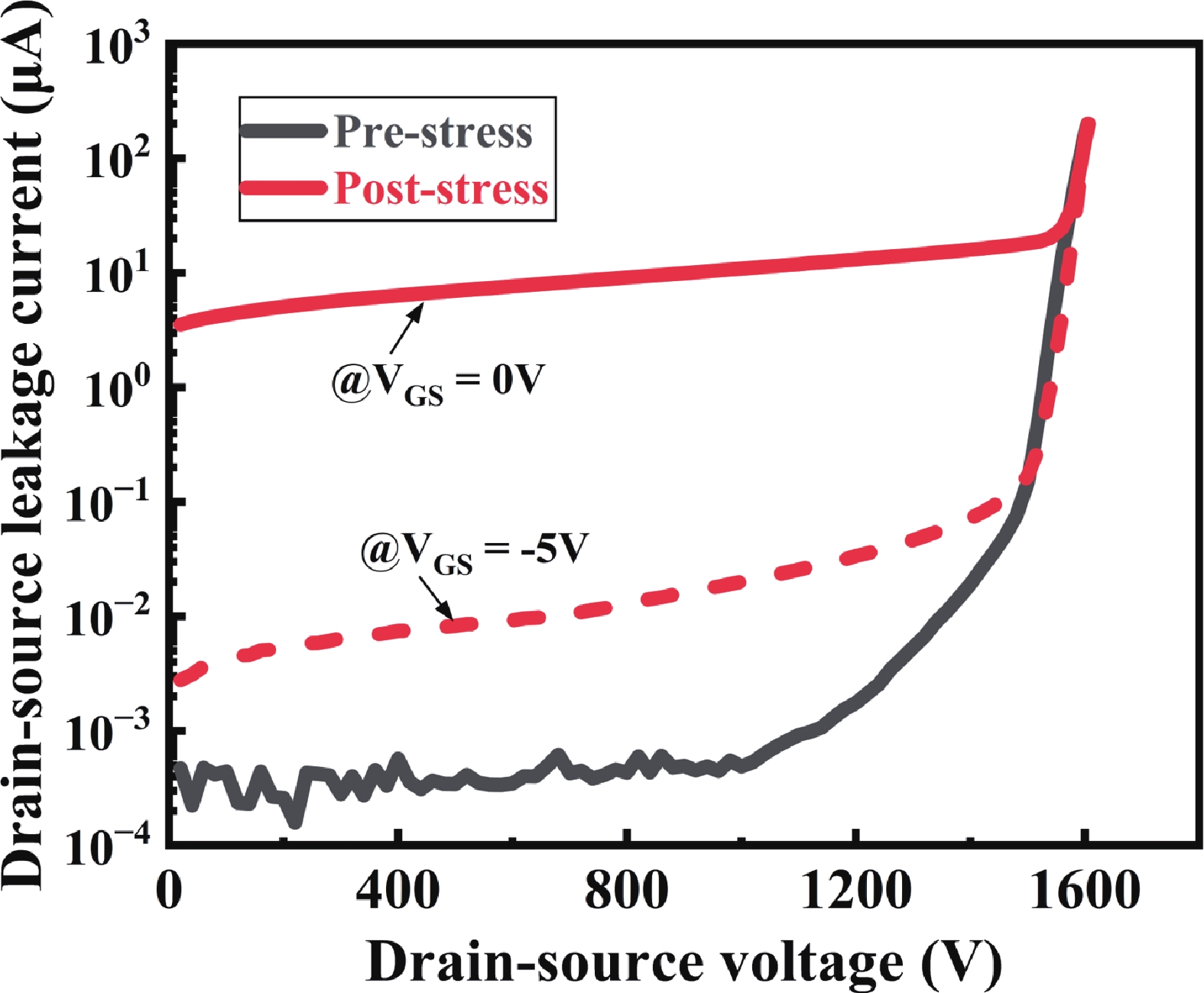
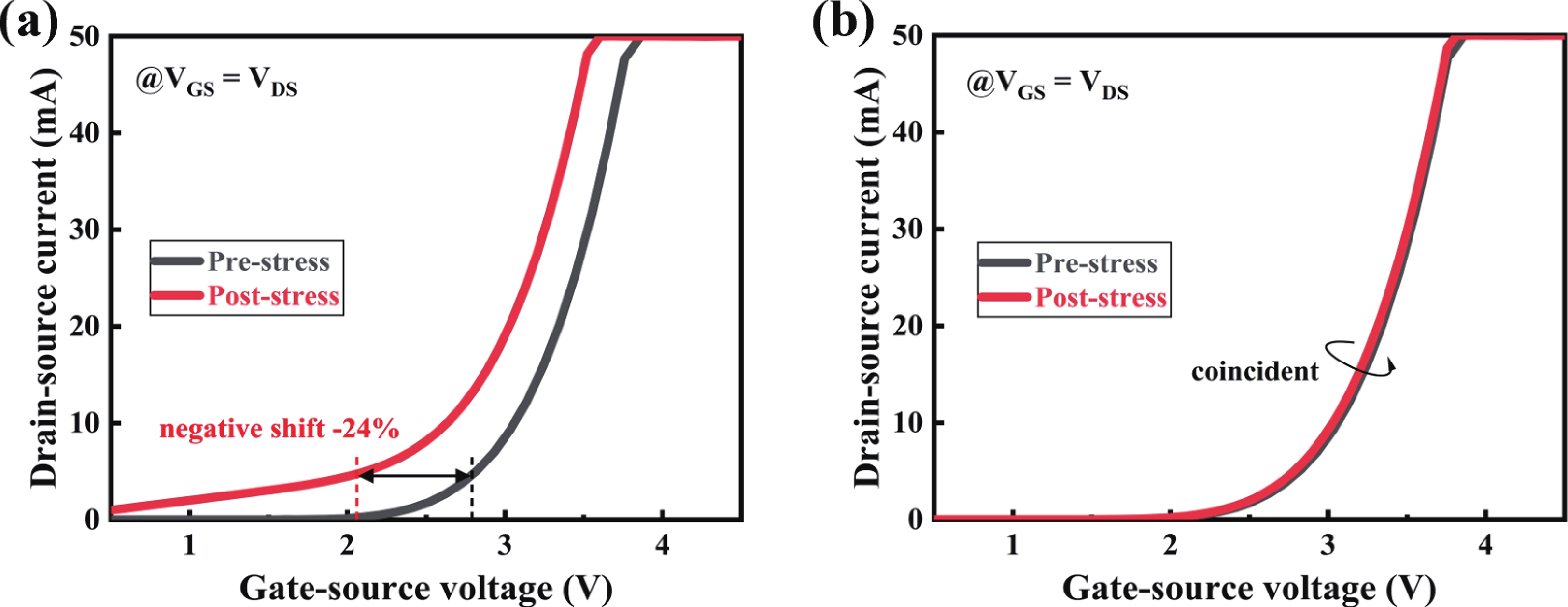
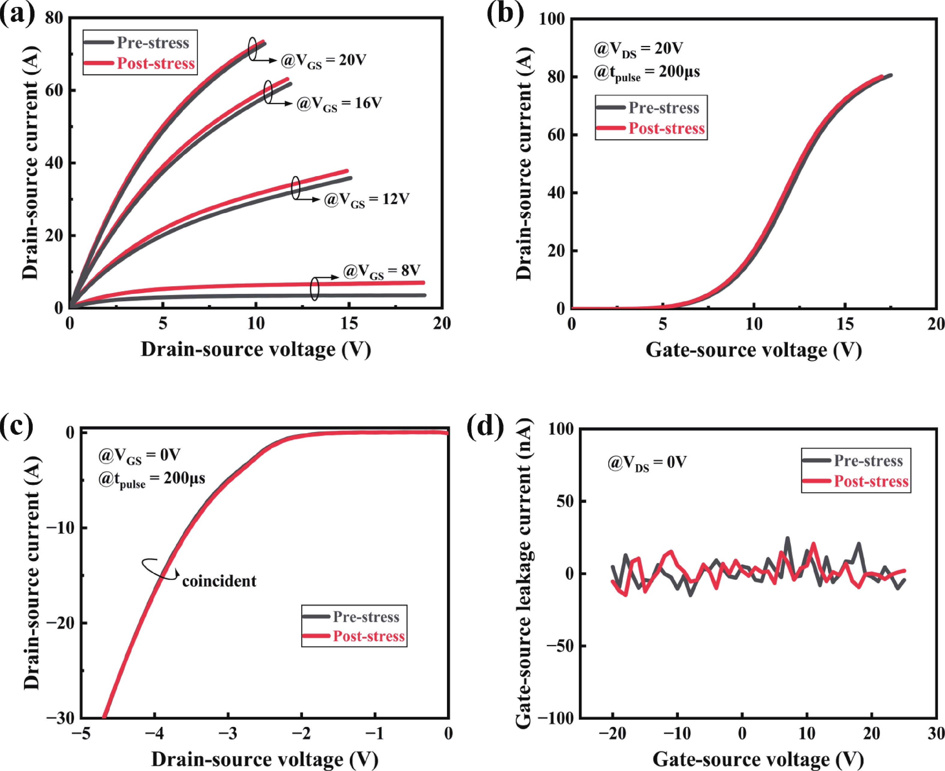
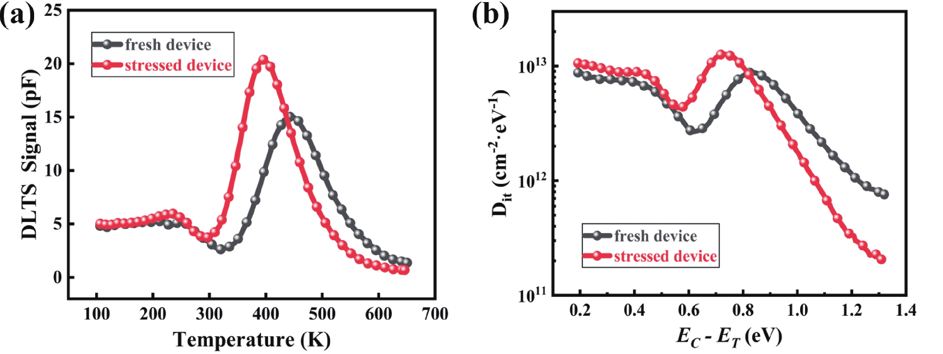
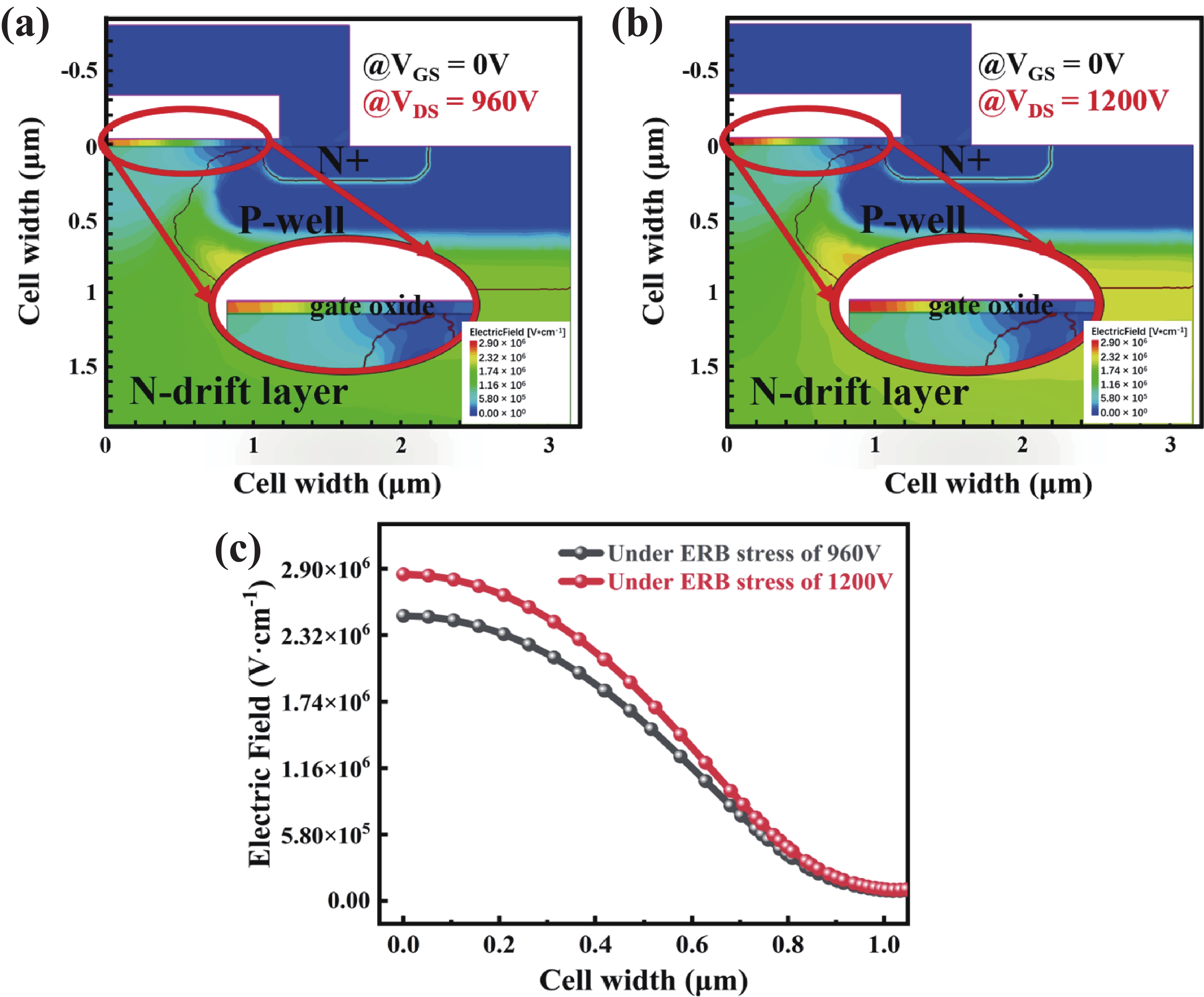
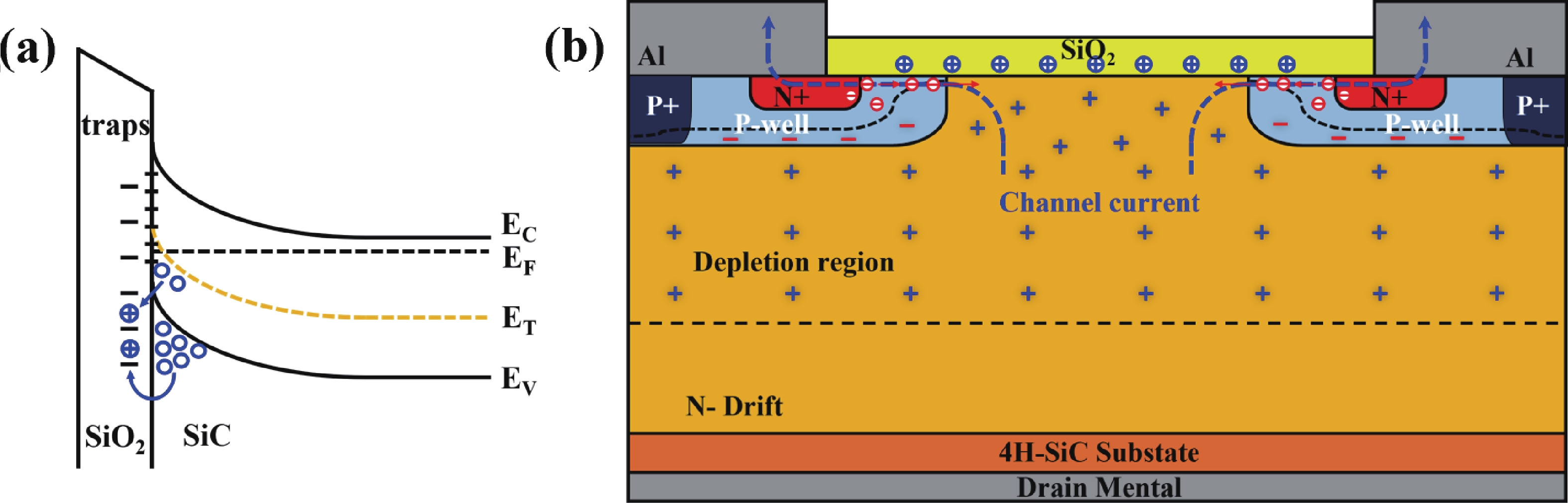
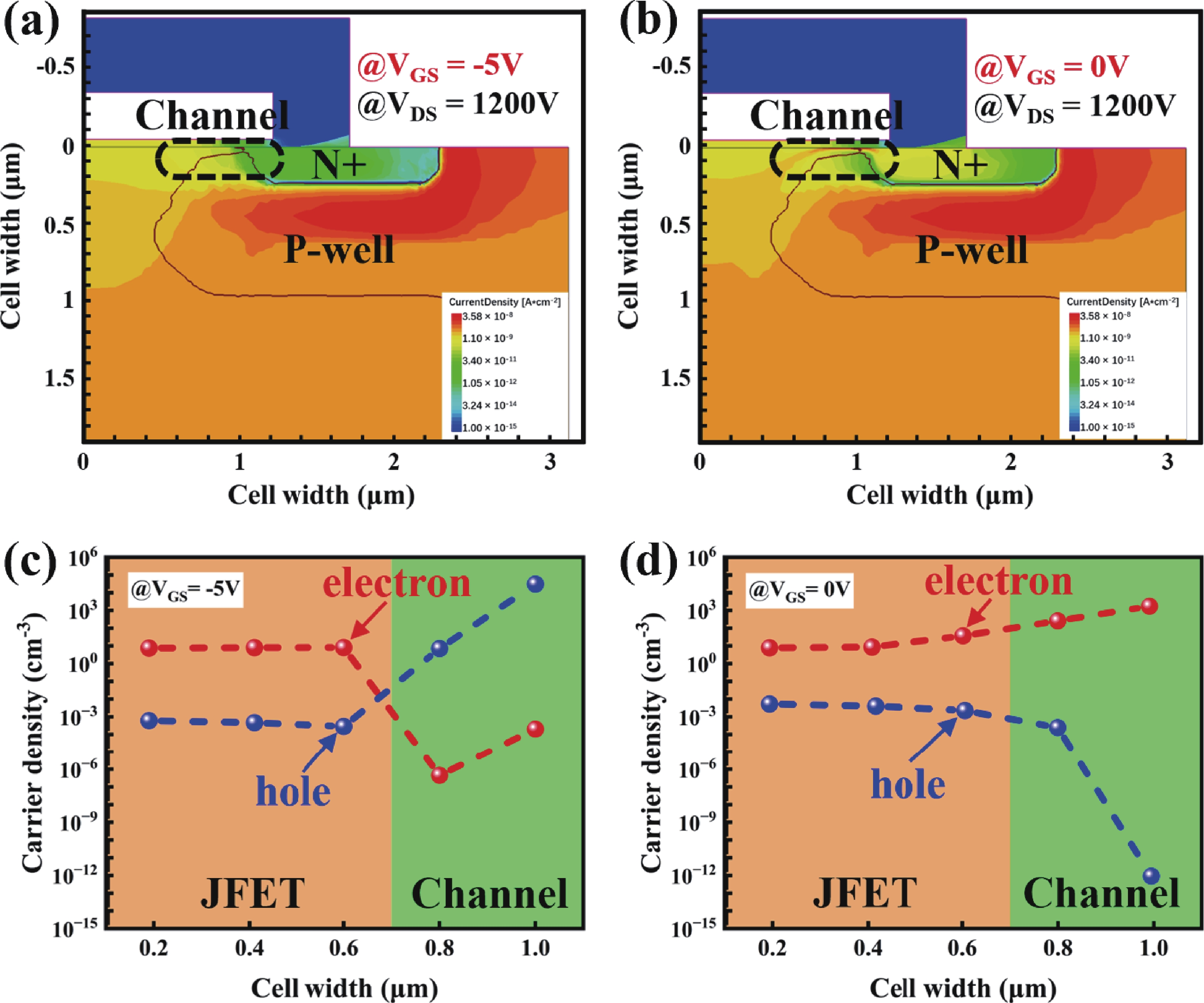
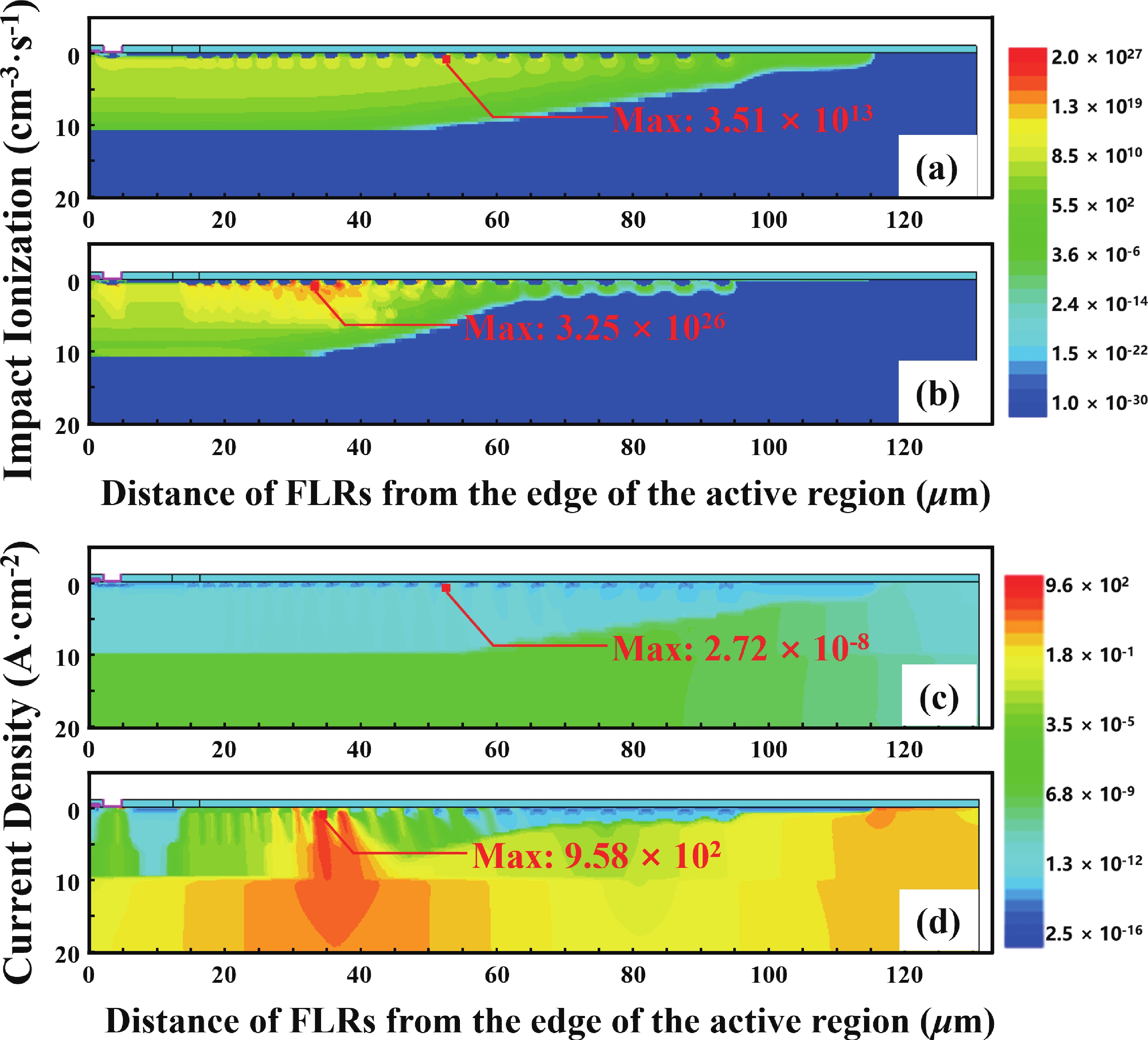
Table 1. Electrical parameters extraction conditions and typical value.
| Parameters | Unit | Extraction conditions | Typical value |
| VBR | V | VGS = 0 V, IDS = 100 μA | 1580 |
| IDSS | nA | VGS = 0 V, VDS = 1200 V | 2.5 |
| RDS,on | mΩ | VGS = 20 V, IDS = 20 A | 83 |
| VGS,th | V | VGS = VDS, IDS = 5 mA | 2.89 |
| VSD | V | VGS = 0 V, IDS = −10 A | −3.60 |
 DownLoad: CSV
| [1] |
She X, Huang A Q, Lucia O, et al. Review of silicon carbide power devices and their applications. IEEE Trans Ind Electron, 2017, 64(10): 8193 doi: 10.1109/TIE.2017.2652401
|
| [2] |
Saito W. A future outlook of power devices from the viewpoint of power electronics trends. IEEE Trans Electron Devices, 2024, 71(3): 1356 doi: 10.1109/TED.2023.3332611
|
| [3] |
Hazra S, De A K, Cheng L, et al. High switching performance of 1700V, 50A SiC power MOSFET over Si IGBT/BiMOSFET for advanced power conversion applications. IEEE Trans Power Electron, 2016, 31(7): 4742 doi: 10.1109/TPEL.2015.2432012
|
| [4] |
Kumar A, Moradpour M, Losito M, et al. Wide band gap devices and their application in power electronics. Energies, 2022, 15(23): 9172 doi: 10.3390/en15239172
|
| [5] |
Millán J, Godignon P, Perpiñà X, et al. A survey of wide bandgap power semiconductor devices. IEEE Trans Power Electron, 2014, 29(5): 2155 doi: 10.1109/TPEL.2013.2268900
|
| [6] |
Wang H, Blaabjerg F. Power electronics reliability: State of the art and outlook. IEEE J Emerg Sel Topics Power Electron, 2021, 9(6): 6476 doi: 10.1109/JESTPE.2020.3037161
|
| [7] |
Lutz J, Schlangenotto H, Scheuermann U, et al. Semiconductor power devices: Physics, characteristics, reliability. Springer, 2011 doi: 10.1007/978-3-319-70917-8
|
| [8] |
Jayant Baliga B. Silicon carbide power devices. World Scientific, 2006 doi: 10.1109/smicnd.1998.732305
|
| [9] |
Yuan X B, Laird I, Walder S. Opportunities, challenges, and potential solutions in the application of fast-switching SiC power devices and converters. IEEE Trans Power Electron, 2021, 36(4): 3925 doi: 10.1109/TPEL.2020.3024862
|
| [10] |
Du Y J, Li J Y, Wang P, et al. Comparison of high voltage SiC MOSFET and Si IGBT power module thermal performance. Mater Sci Forum, 2019, 954: 194 doi: 10.4028/www.scientific.net/MSF.954.194
|
| [11] |
Rahimo M. Performance evaluation and expected challenges of silicon carbide power MOSFETs for high voltage applications. Mater Sci Forum, 2017, 897: 649 doi: 10.4028/www.scientific.net/MSF.897.649
|
| [12] |
Wei J X, Wei Z X, Fu H, et al. Review on the reliability mechanisms of SiC power MOSFETs: A comparison between planar-gate and trench-gate structures. IEEE Trans Power Electron, 2023, 38(7): 8990 doi: 10.1109/TPEL.2023.3265864
|
| [13] |
Salmen P, Friedrichs P. Qualifying a silicon carbide power module: Reliability testing beyond the standards of silicon devices. CIPS 2022; 12th International Conference on Integrated Power Electronics Systems, 2022: 1 doi: https://www.vde-verlag.de/proceedings-de/455757077.html
|
| [14] |
Moultif N, Joubert E, Masmoudi M, et al. Characterization of HTRB stress effects on SiC MOSFETs using photon emission spectral signatures. Microelectron Reliab, 2017, 76: 243 doi: 10.1016/j.microrel.2017.07.013
|
| [15] |
Tang J Y, Duan Y H, Liu P. Investigation of degradation and failure mechanism in 1200 V planar SiC MOSFET under statical accelerated lifetime Test. IEEE Trans Device Mater Relib, 2025, 25(3): 441 doi: 10.1109/TDMR.2025.3577612
|
| [16] |
Matsushima H, Yamada R, Shima A. Two mechanisms of charge accumulation in edge termination of 4H-SiC diodes caused by high-temperature bias stress and high-temperature and high-humidity bias stress. IEEE Trans Electron Devices, 2018, 65(8): 3318 doi: 10.1109/TED.2018.2845376
|
| [17] |
Dong P, Li P, Zhang L, et al. Atomistic mechanism of 4H-SiC/SiO2 interface carrier-trapping effects on breakdown-voltage degradation in power devices. Phys Rev Appl, 2021, 15(3): 034007 doi: 10.1103/PhysRevApplied.15.034007
|
| [18] |
Yu M Y, Shen Y, Ma H P, et al. Experiment and analysis of termination robustness design for 1200 V 4H-SiC MOSFET. Nanomaterials, 2025, 15(11): 805 doi: 10.3390/nano15110805
|
| [19] |
Fiorenza P, Alessandrino M S, Carbone B, et al. Understanding the role of threading dislocations on 4H-SiC MOSFET breakdown under high temperature reverse bias stress. Nanotechnology, 2020, 31(12): 125203 doi: 10.1088/1361-6528/ab5ff6
|
| [20] |
Fiorenza P, Adamo S, Alessandrino M S, et al. Correlation between MOSFETs breakdown and 4H-SiC epitaxial defects. 2021 IEEE International Reliability Physics Symposium (IRPS), 2021: 1 doi: 10.1109/irps46558.2021.9405148
|
| [21] |
Senzaki J, Kojima K, Kato T, et al. Correlation between reliability of thermal oxides and dislocations in n-type 4H-SiC epitaxial wafers. Appl Phys Lett, 2006, 89(2): 022909 doi: 10.1063/1.2221525
|
| [22] |
Jouha W, Masmoudi M, El Oualkadi A, et al. Physical study of SiC power MOSFETs towards HTRB stress based on C-V characteristics. IEEE Trans Device Mater Relib, 2020, 20(3): 506 doi: 10.1109/TDMR.2020.2999029
|
| [23] |
Ren M, Liang S Q, Zhou T, et al. Gate oxide failure mechanisms of SiC MOSFET related to electro-thermomechanical stress under HTRB and HTGB test. 2024 36th International Symposium on Power Semiconductor Devices and ICs (ISPSD), 2024: 208 doi: 10.1109/ispsd59661.2024.10579620
|
| [24] |
Garete A J, Li Z W, Fung Y W, et al. Reliability performance study of molding compounds on high voltage molded leaded package. 2023 18th International Microsystems, Packaging, Assembly and Circuits Technology Conference (IMPACT), 2023: 67 doi: 10.1109/impact59481.2023.10348634
|
| [25] |
Ooi A L, Goh D, Ngwan V C. High temperature reverse bias (HTRB) & temperature humidity bias (THB) reliability failure mechanisms and improvements in trench power MOSFET and IGBT. IEEE J Electron Devices Soc, 2021, 9: 1181 doi: 10.1109/JEDS.2021.3109347
|
| [26] |
Potera R R, Witt T, Zheng Y. Analysis of transient HTRB leakage in a SiC field ring termination. 2020 IEEE International Reliability Physics Symposium (IRPS), 2020: 1 doi: 10.1109/IRPS45951.2020.9129571
|
| [27] |
Aichinger T, Rescher G, Pobegen G. Threshold voltage peculiarities and bias temperature instabilities of SiC MOSFETs. Microelectron Reliab, 2018, 80: 68 doi: 10.1016/j.microrel.2017.11.020
|
| [28] |
JEDEC Solid State Technology Association. JEP-183A: Guidelines for Measuring the Reliability of Solid-State Drives (SSDs). JEDEC Standard, 2023 doi: https://www.jedec.org/
|
| [29] |
Cai J H, Peng Y J, Fan J F, et al. The reverse bias reliability of SiC MOSFET under different conditions and failure analysis. 2024 25th International Conference on Electronic Packaging Technology (ICEPT), 2024: 1 doi: 10.1109/icept63120.2024.10668576
|
| [30] |
Chowdhury S, Matocha K, Powell B, et al. Next generation 1200V, 3.5mΩ∙cm2 SiC planar gate MOSFET with excellent HTRB reliability. 2018 IEEE 30th International Symposium on Power Semiconductor Devices and ICs (ISPSD), 2018: 427 doi: 10.1109/ISPSD.2018.8393694
|
| [31] |
Rudenko T E, Osiyuk I N, Tyagulski I P, et al. Interface trap properties of thermally oxidized n-type 4H–SiC and 6H–SiC. Solid State Electron, 2005, 49(4): 545 doi: 10.1016/j.sse.2004.12.006
|
| [32] |
Jiang S, Zhang M, Meng X W, et al. Trap characterization of trench-gate SiC MOSFETs based on transient drain current. IEEE Trans Power Electron, 2023, 38(5): 6555 doi: 10.1109/TPEL.2023.3242950
|


Article views: 2190 Times PDF downloads: 310 Times Cited by: 0 Times
Received: 26 November 2025 Revised: 28 December 2025 Online: Accepted Manuscript: 15 January 2026Uncorrected proof: 22 January 2026Published: 21 April 2026
| Citation: |
Fanpeng Zeng, Yingxin Cui, Zhixin Liu, Zicheng Lu, Lingling Lai, Shoulai Gong, Haochen Wang, Peng Dong, Jisheng Han. Gate oxide damage and synergistic effect on the breakdown voltage under reverse bias stress for SiC MOSFET[J]. Journal of Semiconductors, 2026, 47(4): 042501. doi: 10.1088/1674-4926/25110026
****
F P Zeng, Y X Cui, Z X Liu, Z C Lu, L L Lai, S L Gong, H C Wang, P Dong, and J S Han, Gate oxide damage and synergistic effect on the breakdown voltage under reverse bias stress for SiC MOSFET[J]. J. Semicond., 2026, 47(4): 042501 doi: 10.1088/1674-4926/25110026

|
 Fanpeng Zeng got his bachelor’s degree in 2018 from Yanshan University and his master’s degree in 2024 from Shandong University. Now he is a doctoral student at Shandong University under the supervision of Prof. Yingxin Cui and Prof. Jisheng Han. His research focuses on the reliability study of silicon carbide power devices
 Yingxin Cui received her doctoral degree from Shandong University, Jinan, China, in 2016. She is currently a Professor with the Institute of novel semiconductors, Shandong University, Jinan, China. Her current research interests include the material defects in silicon carbide, high reliability silicon carbide power devices and power modules
 Peng Dong received his doctoral degree from Zhejiang University, Hangzhou, China, in 2015. He is currently an Associate Research Fellow with the Microsystem and Terahertz Research Center, Institute of Electronic Engineering, China Academy of Engineering Physics, Mianyang, China. His current research interests are focused on the reliability and defects engineering of power devices
| [1] |
She X, Huang A Q, Lucia O, et al. Review of silicon carbide power devices and their applications. IEEE Trans Ind Electron, 2017, 64(10): 8193 doi: 10.1109/TIE.2017.2652401
|
| [2] |
Saito W. A future outlook of power devices from the viewpoint of power electronics trends. IEEE Trans Electron Devices, 2024, 71(3): 1356 doi: 10.1109/TED.2023.3332611
|
| [3] |
Hazra S, De A K, Cheng L, et al. High switching performance of 1700V, 50A SiC power MOSFET over Si IGBT/BiMOSFET for advanced power conversion applications. IEEE Trans Power Electron, 2016, 31(7): 4742 doi: 10.1109/TPEL.2015.2432012
|
| [4] |
Kumar A, Moradpour M, Losito M, et al. Wide band gap devices and their application in power electronics. Energies, 2022, 15(23): 9172 doi: 10.3390/en15239172
|
| [5] |
Millán J, Godignon P, Perpiñà X, et al. A survey of wide bandgap power semiconductor devices. IEEE Trans Power Electron, 2014, 29(5): 2155 doi: 10.1109/TPEL.2013.2268900
|
| [6] |
Wang H, Blaabjerg F. Power electronics reliability: State of the art and outlook. IEEE J Emerg Sel Topics Power Electron, 2021, 9(6): 6476 doi: 10.1109/JESTPE.2020.3037161
|
| [7] |
Lutz J, Schlangenotto H, Scheuermann U, et al. Semiconductor power devices: Physics, characteristics, reliability. Springer, 2011 doi: 10.1007/978-3-319-70917-8
|
| [8] |
Jayant Baliga B. Silicon carbide power devices. World Scientific, 2006 doi: 10.1109/smicnd.1998.732305
|
| [9] |
Yuan X B, Laird I, Walder S. Opportunities, challenges, and potential solutions in the application of fast-switching SiC power devices and converters. IEEE Trans Power Electron, 2021, 36(4): 3925 doi: 10.1109/TPEL.2020.3024862
|
| [10] |
Du Y J, Li J Y, Wang P, et al. Comparison of high voltage SiC MOSFET and Si IGBT power module thermal performance. Mater Sci Forum, 2019, 954: 194 doi: 10.4028/www.scientific.net/MSF.954.194
|
| [11] |
Rahimo M. Performance evaluation and expected challenges of silicon carbide power MOSFETs for high voltage applications. Mater Sci Forum, 2017, 897: 649 doi: 10.4028/www.scientific.net/MSF.897.649
|
| [12] |
Wei J X, Wei Z X, Fu H, et al. Review on the reliability mechanisms of SiC power MOSFETs: A comparison between planar-gate and trench-gate structures. IEEE Trans Power Electron, 2023, 38(7): 8990 doi: 10.1109/TPEL.2023.3265864
|
| [13] |
Salmen P, Friedrichs P. Qualifying a silicon carbide power module: Reliability testing beyond the standards of silicon devices. CIPS 2022; 12th International Conference on Integrated Power Electronics Systems, 2022: 1 doi: https://www.vde-verlag.de/proceedings-de/455757077.html
|
| [14] |
Moultif N, Joubert E, Masmoudi M, et al. Characterization of HTRB stress effects on SiC MOSFETs using photon emission spectral signatures. Microelectron Reliab, 2017, 76: 243 doi: 10.1016/j.microrel.2017.07.013
|
| [15] |
Tang J Y, Duan Y H, Liu P. Investigation of degradation and failure mechanism in 1200 V planar SiC MOSFET under statical accelerated lifetime Test. IEEE Trans Device Mater Relib, 2025, 25(3): 441 doi: 10.1109/TDMR.2025.3577612
|
| [16] |
Matsushima H, Yamada R, Shima A. Two mechanisms of charge accumulation in edge termination of 4H-SiC diodes caused by high-temperature bias stress and high-temperature and high-humidity bias stress. IEEE Trans Electron Devices, 2018, 65(8): 3318 doi: 10.1109/TED.2018.2845376
|
| [17] |
Dong P, Li P, Zhang L, et al. Atomistic mechanism of 4H-SiC/SiO2 interface carrier-trapping effects on breakdown-voltage degradation in power devices. Phys Rev Appl, 2021, 15(3): 034007 doi: 10.1103/PhysRevApplied.15.034007
|
| [18] |
Yu M Y, Shen Y, Ma H P, et al. Experiment and analysis of termination robustness design for 1200 V 4H-SiC MOSFET. Nanomaterials, 2025, 15(11): 805 doi: 10.3390/nano15110805
|
| [19] |
Fiorenza P, Alessandrino M S, Carbone B, et al. Understanding the role of threading dislocations on 4H-SiC MOSFET breakdown under high temperature reverse bias stress. Nanotechnology, 2020, 31(12): 125203 doi: 10.1088/1361-6528/ab5ff6
|
| [20] |
Fiorenza P, Adamo S, Alessandrino M S, et al. Correlation between MOSFETs breakdown and 4H-SiC epitaxial defects. 2021 IEEE International Reliability Physics Symposium (IRPS), 2021: 1 doi: 10.1109/irps46558.2021.9405148
|
| [21] |
Senzaki J, Kojima K, Kato T, et al. Correlation between reliability of thermal oxides and dislocations in n-type 4H-SiC epitaxial wafers. Appl Phys Lett, 2006, 89(2): 022909 doi: 10.1063/1.2221525
|
| [22] |
Jouha W, Masmoudi M, El Oualkadi A, et al. Physical study of SiC power MOSFETs towards HTRB stress based on C-V characteristics. IEEE Trans Device Mater Relib, 2020, 20(3): 506 doi: 10.1109/TDMR.2020.2999029
|
| [23] |
Ren M, Liang S Q, Zhou T, et al. Gate oxide failure mechanisms of SiC MOSFET related to electro-thermomechanical stress under HTRB and HTGB test. 2024 36th International Symposium on Power Semiconductor Devices and ICs (ISPSD), 2024: 208 doi: 10.1109/ispsd59661.2024.10579620
|
| [24] |
Garete A J, Li Z W, Fung Y W, et al. Reliability performance study of molding compounds on high voltage molded leaded package. 2023 18th International Microsystems, Packaging, Assembly and Circuits Technology Conference (IMPACT), 2023: 67 doi: 10.1109/impact59481.2023.10348634
|
| [25] |
Ooi A L, Goh D, Ngwan V C. High temperature reverse bias (HTRB) & temperature humidity bias (THB) reliability failure mechanisms and improvements in trench power MOSFET and IGBT. IEEE J Electron Devices Soc, 2021, 9: 1181 doi: 10.1109/JEDS.2021.3109347
|
| [26] |
Potera R R, Witt T, Zheng Y. Analysis of transient HTRB leakage in a SiC field ring termination. 2020 IEEE International Reliability Physics Symposium (IRPS), 2020: 1 doi: 10.1109/IRPS45951.2020.9129571
|
| [27] |
Aichinger T, Rescher G, Pobegen G. Threshold voltage peculiarities and bias temperature instabilities of SiC MOSFETs. Microelectron Reliab, 2018, 80: 68 doi: 10.1016/j.microrel.2017.11.020
|
| [28] |
JEDEC Solid State Technology Association. JEP-183A: Guidelines for Measuring the Reliability of Solid-State Drives (SSDs). JEDEC Standard, 2023 doi: https://www.jedec.org/
|
| [29] |
Cai J H, Peng Y J, Fan J F, et al. The reverse bias reliability of SiC MOSFET under different conditions and failure analysis. 2024 25th International Conference on Electronic Packaging Technology (ICEPT), 2024: 1 doi: 10.1109/icept63120.2024.10668576
|
| [30] |
Chowdhury S, Matocha K, Powell B, et al. Next generation 1200V, 3.5mΩ∙cm2 SiC planar gate MOSFET with excellent HTRB reliability. 2018 IEEE 30th International Symposium on Power Semiconductor Devices and ICs (ISPSD), 2018: 427 doi: 10.1109/ISPSD.2018.8393694
|
| [31] |
Rudenko T E, Osiyuk I N, Tyagulski I P, et al. Interface trap properties of thermally oxidized n-type 4H–SiC and 6H–SiC. Solid State Electron, 2005, 49(4): 545 doi: 10.1016/j.sse.2004.12.006
|
| [32] |
Jiang S, Zhang M, Meng X W, et al. Trap characterization of trench-gate SiC MOSFETs based on transient drain current. IEEE Trans Power Electron, 2023, 38(5): 6555 doi: 10.1109/TPEL.2023.3242950
|

 WeChat ID
Journal of Semiconductors © 2017 All Rights Reserved 京ICP备05085259号-2