


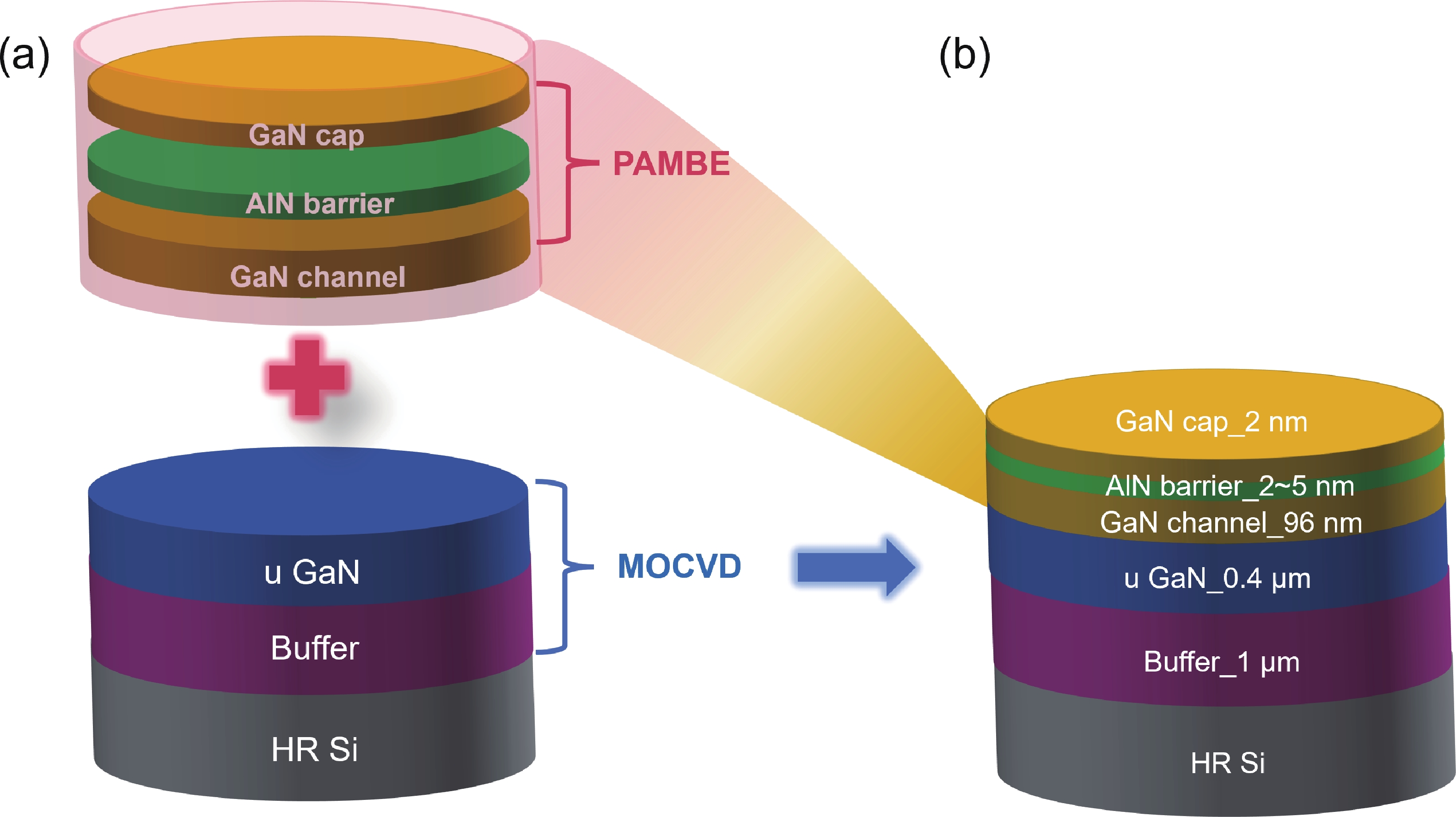
Fig. 1.
(Color online) Schematic of the epitaxial growth process. (a) MOCVD-grown GaN template on 6-inch Si substrate; (b) PAMBE-grown active layers on GaN template.
ARTICLES
Li Liu1, §, Hanxiang Jia1, §, Jiajie Pan1, 2, Hao Ying1, Yiyuan Sun1, Lei Pan1, Bo Zhao1, Jun Liu1, and Shuangzan Lu1,
Corresponding author: Jun Liu, liujun@jfslab.com.cn; Shuangzan Lu, lushuangzan@jfslab.com.cn
Abstract: AlN/GaN high-electron-mobility transistor (HEMT) equipped with ultra-thin AlN barrier epitaxial structures were grown on 6-inch and 8-inch Si-based GaN templates via plasma-assisted molecular beam epitaxy (PAMBE). The AlN barrier thickness was systematically optimized to improve the properties of two-dimensional electron gas (2DEG). Structural and electrical characterizations were performed by atomic force microscopy (AFM), transmission electron microscopy (TEM), contact and non-contact Hall measurements. At an optimal AlN barrier thickness, an extremely low sheet resistance of 159.9 Ω/□ by contact Hall and 143.8 Ω/□ by non-contact Hall was achieved on the 6-inch HEMT wafer, marking a significant improvement over state-of-the-art Si-based GaN HEMTs. The epitaxial surface exhibited excellent morphology with a root-mean-square (RMS) roughness of 0.45 nm. Moreover, cross-sectional TEM analysis of PAMBE-grown AlN/GaN HEMT revealed an atomically sharp and structurally coherent heterointerface, which is critical for achieving high electron mobility and reduced scattering loss. In addition, the 8-inch HEMT demonstrated a sheet resistance (Rs) as low as 115 Ω/□ by non-contact Hall with a uniformity of 2.13%, outperforming competing technologies from other companies on the market.
Keywords: PAMBE, HEMT, ultra-thin AlN barrier, sheet resistance, 2DEG
| [1] |
Ganguly S, Song B, Hwang W S, et al. AlGaN/GaN HEMTs on Si by MBE with regrown contacts and fT = 153 GHz. Phys Status Solidi C, 2014, 11(3/4): 887 doi: 10.1002/pssc.201300668
|
| [2] |
Pavlidis D, Valizadeh P, Hsu S H, et al. AlGaN/GaN high electron mobility transistor (HEMT) reliability. Proc Eur Gallium Arsenide and Other Semiconductor, Appl Symp GAAS 2005, 2005: 265
|
| [3] |
Narang K, Bag R K, Singh V K, et al. Improvement in surface morphology and 2DEG properties of AlGaN/GaN HEMT. J Alloys Compd, 2020, 815: 152283 doi: 10.1016/j.jallcom.2019.152283
|
| [4] |
Chu J Y, Wang Q, Jiang L J, et al. Room temperature 2DEG mobility above 2350 cm2/(V·s) in AlGaN/GaN HEMT grown on GaN substrate. J Electron Mater, 2021, 50(5): 2630 doi: 10.1007/s11664-021-08778-y
|
| [5] |
Kharei P, Baidya A, Maity N P, et al. An insight to current collapse in GaN HEMT and suppressing techniques. Eng Res Express, 2023, 5(1): 01200 doi: 10.1088/2631-8695/acb131
|
| [6] |
Fang T, Wang R H, Xing H L, et al. Effect of optical phonon scattering on the performance of GaN transistors. IEEE Electron Device Lett, 2012, 33(5): 709 doi: 10.1109/LED.2012.2187169
|
| [7] |
Wu Y R, Singh M, Singh J. Sources of transconductance collapse in III-V nitrides-consequences of velocity-field relations and source/gate design. IEEE Trans Electron Devices, 2005, 52(6): 1048 doi: 10.1109/TED.2005.848084
|
| [8] |
Palacios T, Rajan S, Chakraborty A, et al. Influence of the dynamic access resistance in the gm and fT linearity of AlGaN/GaN HEMTs. IEEE Trans Electron Devices, 2005, 52(10): 2117 doi: 10.1109/TED.2005.856180
|
| [9] |
Haziq M, Falina S, Manaf A A, et al. Syamsul, challenges and opportunities for high-power and high-frequency AlGaN/GaN high-electron-mobility transistor (HEMT) applications: A review, micromachines. Micromachines, 2022, 13: 2133 doi: 10.3390/mi13122133
|
| [10] |
Wang Q, Chen C X, Li W, et al. Fabrication and characterization of AlGaN/GaN HEMTs with high power gain and efficiency at 8 GHz. J Semicond, 2021, 42(12): 122802 doi: 10.1088/1674-4926/42/12/122802
|
| [11] |
Liu S Y, Zhu J J, Guo J S, et al. Low-damage interface enhancement-mode AlN/GaN high electron mobility transistors with 41.6% PAE at 30 GHz. Chin Phys B, 2023, 32(11): 117302 doi: 10.1088/1674-1056/acd8a5
|
| [12] |
Kim S, Kim E, Walwil H, et al. Thermal characterization and design of AlN/GaN/AlN HEMTs on foreign substrates. IEEE Electron Device Lett, 2025, 46(5): 817 doi: 10.1109/LED.2025.3548853
|
| [13] |
Wang X L, Chen T S, Xiao H L, et al. An internally-matched GaN HEMTs device with 45.2W at 8GHz for X-band application. Solid State Electron, 2009, 53(3): 332 doi: 10.1016/j.sse.2009.01.003
|
| [14] |
Cao Y, Zimmermann T, Deen D, et al. Ultrathin MBE-grown AlN/GaN HEMTs with record high current densities. 2007 International Semiconductor Device Research Symposium, 2008: 1 doi: 10.1109/ISDRS.2007.4422436
|
| [15] |
Shen L, Heikman S, Moran B, et al. AlGaN/AlN/GaN high-power microwave HEMT. IEEE Electron Device Lett, 2001, 22(10): 457 doi: 10.1109/55.954910
|
| [16] |
Chen S T, Chen Q S, Ye F, et al. Epitaxial growth of a high-quality GaN/AlN heterostructure for the development of an AlN-back barrier high-electron-mobility-transistor. CrystEngComm, 2025, 27(23): 4011 doi: 10.1039/D5CE00205B
|
| [17] |
Kong X, Wei K, Liu G G, et al. Improved performance of highly scaled AlGaN/GaN high-electron-mobility transistors using an AlN back barrier. Appl Phys Express, 2013, 6(5): 051201 doi: 10.7567/APEX.6.051201
|
| [18] |
Yu Q, Shi C Z, Yang L, et al. Improved DC and RF characteristics of gan-based double-channel HEMTs by ultra-thin AlN back barrier layer, micromachines. Micromachines, 2024, 15: 1220 doi: 10.3390/mi15101220
|
| [19] |
Zhang H C, Zhang M S, Wang H, et al. Thick-AlN-barrier AlN/GaN-based HEMTs with superior power and noise performance for low-voltage RF front-end applications. Appl Phys Lett, 2025, 126(12): 122103 doi: 10.1063/5.0257620
|
| [20] |
Guo J S, Zhu J J, Liu S Y, et al. Tri-gate normally-off AlN/GaN HEMTs with 2.36 W/mm of power density and 67. 5% power-added-efficiency at vd = 12 V. IEEE Electron Device Lett, 2023, 44(4): 590 doi: 10.1109/LED.2023.3248277
|
| [21] |
Reilly C E, Hatui N, Mates T E, et al. 2DEGs formed in AlN/GaN HEMT structures with AlN grown at low temperature. Appl Phys Lett, 2021, 118(22): 222103 doi: 10.1063/5.0050584
|
| [22] |
Cordier Y, Azize M, Baron N, et al. Subsurface Fe-doped semi-insulating GaN templates for inhibition of regrowth interface pollution in AlGaN/GaN HEMT structures. J Cryst Growth, 2008, 310(5): 948 doi: 10.1016/j.jcrysgro.2007.11.161
|
| [23] |
Kneissl M, Kolbe T, Chua C, et al. Advances in group III-nitride-based deep UV light-emitting diode technology. Semicond Sci Technol, 2011, 26(1): 014036 doi: 10.1088/0268-1242/26/1/014036
|
| [24] |
Mickevičius J, Tamulaitis G, Shur M, et al. Internal quantum efficiency in AlGaN with strong carrier localization. Appl Phys Lett, 2012, 101(21): 211902 doi: 10.1063/1.4767657
|
| [25] |
Ban K, Yamamoto J I, Takeda K, et al. Internal quantum efficiency of whole-composition-range AlGaN multiquantum wells. Appl Phys Express, 2011, 4(5): 052101 doi: 10.1143/APEX.4.052101
|
| [26] |
Godejohann B J, Ture E, Müller S, et al. AlN/GaN HEMTs grown by MBE and MOCVD: Impact of Al distribution. Phys Status Solidi B, 2017, 254(8): 1600715 doi: 10.1002/pssb.201600715
|
| [27] |
Faria F A, Nomoto K, Hu Z Y, et al. Low temperature AlN growth by MBE and its application in HEMTs. J Cryst Growth, 2015, 425: 133 doi: 10.1016/j.jcrysgro.2015.03.039
|
| [28] |
Hwang J, Schaff W J, Green B M, et al. Effects of a molecular beam epitaxy grown AlN passivation layer on AlGaN/GaN heterojunction field effect transistors. Solid State Electron, 2004, 48(2): 363 doi: 10.1016/S0038-1101(03)00324-1
|
| [29] |
Sze S M, Ng K K. Physics of semiconductor devices, 3rd ed. Hoboken, NJ: John Wiley & Sons, 2007
|
| [30] |
Smorchkova I P, Keller S, Heikman S, et al. Two-dimensional electron-gas AlN/GaN heterostructures with extremely thin AlN barriers. Appl Phys Lett, 2000, 77(24): 3998 doi: 10.1063/1.1332408
|
| [31] |
Smorchkova I P, Chen L, Mates T, et al. AlN/GaN and (Al, Ga)N/AlN/GaN two-dimensional electron gas structures grown by plasma-assisted molecular-beam epitaxy. J Appl Phys, 2001, 90(10): 5196 doi: 10.1063/1.1412273
|
| [32] |
Kaun S W. Growth optimization of metal-polar III-nitride high-electron-mobility transistor structures by molecular beam epitaxy. Ph. D. Dissertation, University of California, Santa Barbara, USA, 2014
|
| [33] |
Gau M H, Chen Y L, Hsieh C H, et al. Influence of threading dislocation scattering on the electron mobility in AlGaN/GaN heterostructures grown by PAMBE. Proc APS March Meet, 2006 doi: https://meetings.aps.org/Meeting/MAR07/Session/C1.230
|
| [34] |
Hájek F, Hospodková A, Hubík P, et al. Transport properties of AlGaN/GaN HEMT structures with back barrier: Impact of dislocation density and improved design. Semicond Sci Technol, 2021, 36(7): 075016 doi: 10.1088/1361-6641/abfe9b
|
| [35] |
Zhang L, Cheng Z, He Y W, et al. Optimization of selective-area regrown n-GaN via MOCVD for high-frequency HEMT. Appl Phys Lett, 2021, 119(26): 262104 doi: 10.1063/5.0077937
|
| [36] |
Then H W, Radosavljevic M, Yu Q, et al. Enhancement-mode 300-mm GaN-on-Si(111) with integrated Si CMOS for future mm-wave RF applications. IEEE Microw Wireless Tech Lett, 2023, 33(6): 835 doi: 10.1109/LMWT.2023.3268184
|
| [37] |
Cheng K, Liang H, Van Hove M, et al. AlGaN/GaN/AlGaN double heterostructures grown on 200 mm silicon (111) substrates with high electron mobility. Appl Phys Express, 2012, 5(1): 011002 doi: 10.1143/APEX.5.011002
|
| [38] |
Hickman A, Chaudhuri R, Li L, et al. First RF power operation of AlN/GaN/AlN HEMTs with > 3 A/mm and 3 W/mm at 10 GHz. IEEE J Electron Devices Soc, 2021, 9: 121 doi: 10.1109/JEDS.2020.3042050
|
| [39] |
Harrouche K, Kabouche R, Okada E, et al. High performance and highly robust AlN/GaN HEMTs for millimeter-wave operation. IEEE J Electron Devices Soc, 2019, 7: 1145 doi: 10.1109/JEDS.2019.2952314
|
| [40] |
Rzin M, Meneghini M, Rampazzo F, et al. Linearity and robustness evaluation of 150-nm AlN/GaN HEMTs. Microelectron Reliab, 2019, 100: 113388 doi: 10.1016/j.microrel.2019.06.080
|
| [41] |
Tang Y, Shinohara K, Regan D, et al. Ultrahigh-speed GaN high-electron-mobility transistors with fT/fmax of 454/444 GHz. IEEE Electron Device Lett, 2015, 36: 549 doi: 10.1109/LED.2015.2421311
|
| [42] |
Yang L Y, Wang J L, Sheng S S, et al. Low-resistive ohmic contacts in high-electron-mobility AlN/GaN heterostructures by suppressing the oxygen incorporation. ACS Appl Electron Mater, 2022, 4(7): 3632 doi: 10.1021/acsaelm.2c00585
|
| [43] |
Zimmermann T, Deen D, Cao Y, et al. AlN/GaN insulated-gate HEMTs with 2.3 A/mm output current and 480 mS/mm transconductance. IEEE Electron Device Lett, 2008, 29(7): 661 doi: 10.1109/LED.2008.923318
|
| [44] |
Cao Y, Wang K J, Li G W, et al. MBE growth of high conductivity single and multiple AlN/GaN heterojunctions. J Cryst Growth, 2011, 323(1): 529 doi: 10.1016/j.jcrysgro.2010.12.047
|
| [45] |
Zheng X X, Lin C H, Ueda D, et al. Effects of the growth temperature on structural and electrical properties of AlN/GaN heterostructures grown by metal organic chemical vapor deposition. Thin Solid Films, 2020, 709: 138228 doi: 10.1016/j.tsf.2020.138228
|
| [46] |
Xia Y Y, Zhu Y H, Liu C H, et al. Effects of the cap layer on the properties of AlN barrier HEMT grown on 6-inch Si (111) substrate. Mater Res Express, 2020, 7(6): 065902 doi: 10.1088/2053-1591/ab96f5
|
| [47] |
Yang L Y, Wang X Q, Wang T, et al. Three subband occupation of the two-dimensional electron gas in ultrathin barrier AlN/GaN heterostructures. Adv Funct Mater, 2020, 30(46): 2004450 doi: 10.1002/adfm.202004450
|
| [48] |
Deen D A, Storm D F, Katzer D S, et al. Dependence of ohmic contact resistance on barrier thickness of AlN/GaN HEMT structures. Solid State Electron, 2010, 54(6): 613 doi: 10.1016/j.sse.2009.11.012
|
| [49] |
Bairamis A, Zervos C, Adikimenakis A, et al. Electron density and currents of AlN/GaN high electron mobility transistors with thin GaN/AlN buffer layer. Appl Phys Lett, 2014, 105(11): 113508 doi: 10.1063/1.4896026
|
| [50] |
Harrouche K, Kabouche R, Okada E, et al. High power AlN/GaN HEMTs with record power-added-efficiency >70% at 40 GHz. 2020 IEEE/MTTS Int Microw Symp IMS, 2020: 285 doi: 10.1109/IMS30576.2020.9223971
|
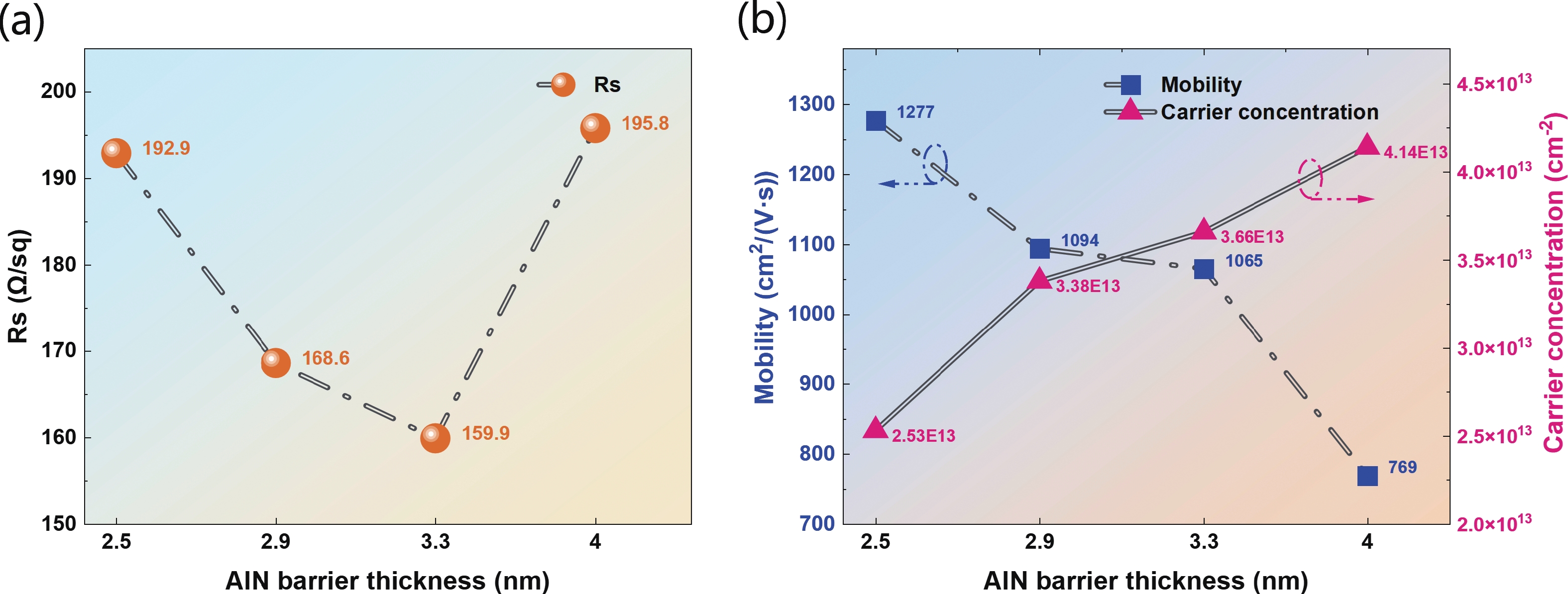
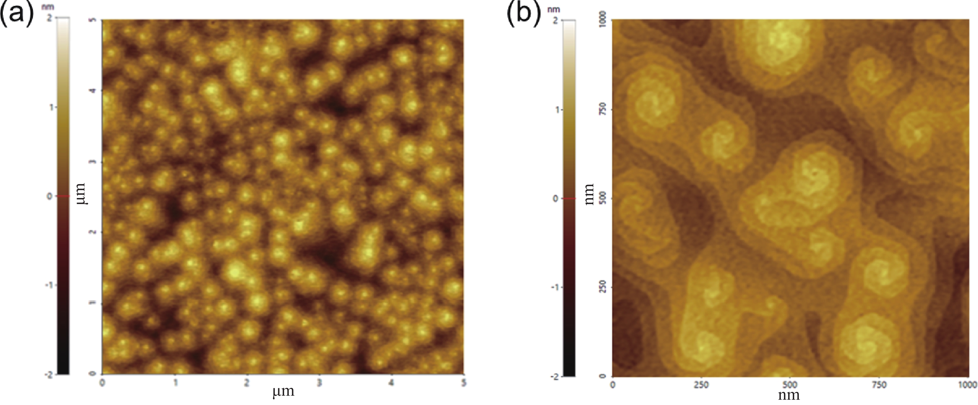
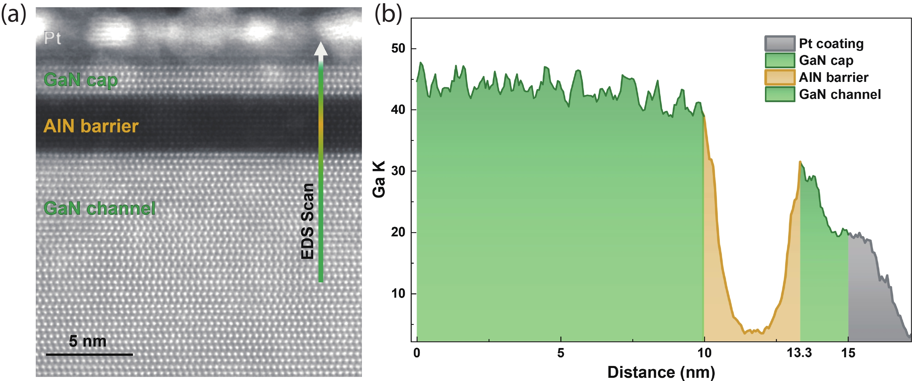
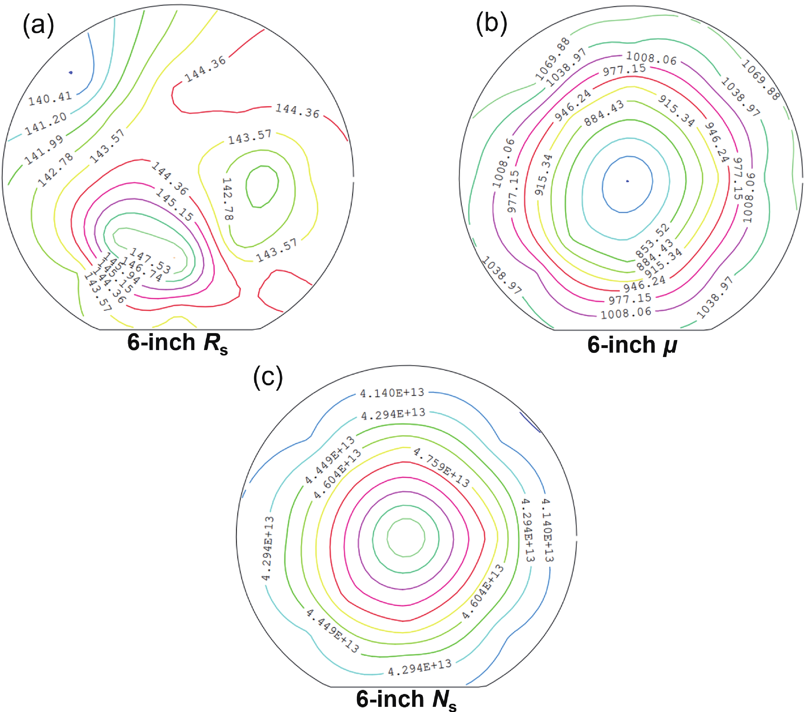
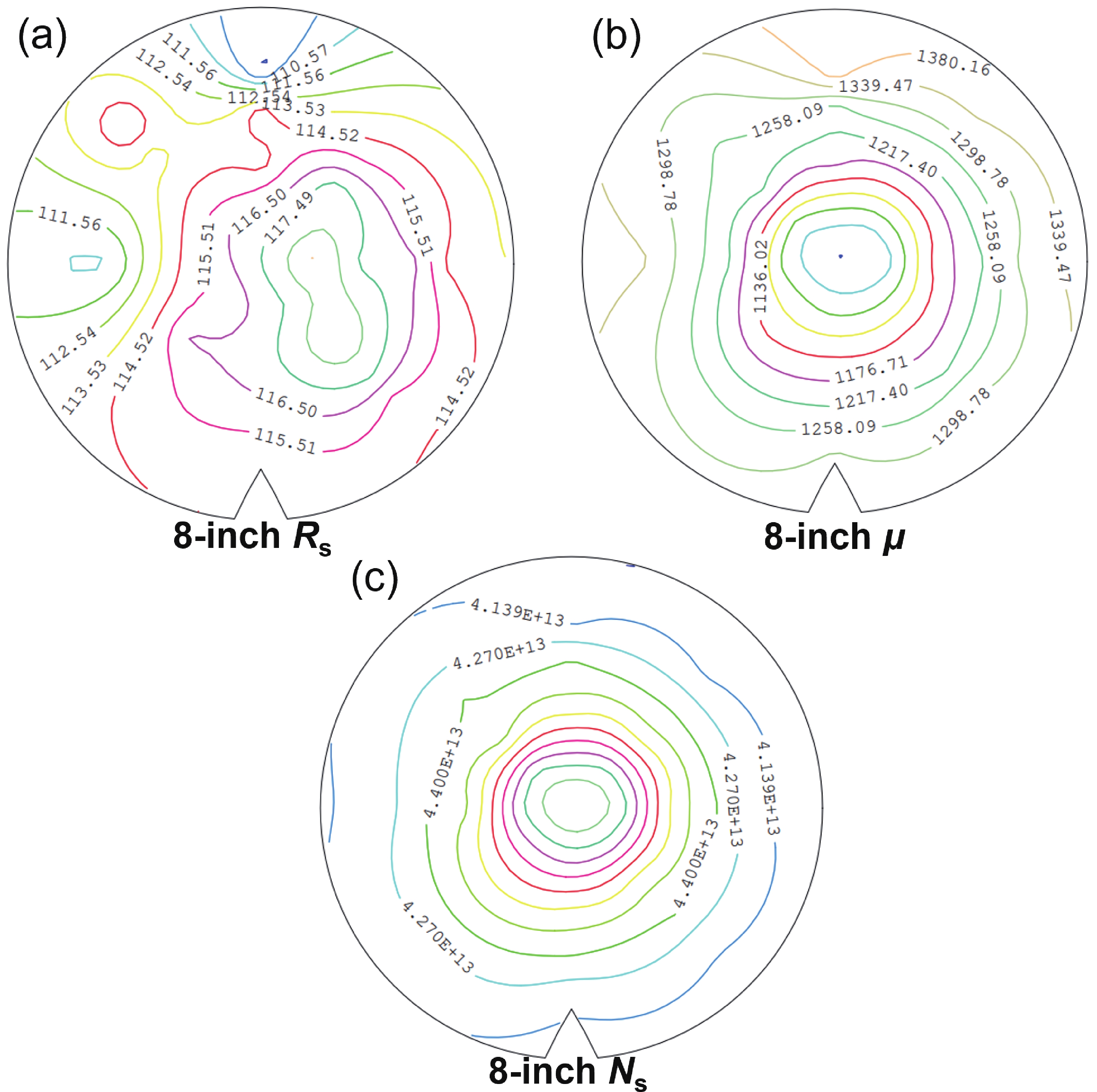
Table 1. Contact-Hall results of as-prepared four samples.
| No. | AlN barrier growth time (s) |
AlN barrier thickness (nm) |
Rs (Ω/□) | Mobility (cm2/(V·s)) |
Carrier concentration (1013 cm−2) |
| Sample A | 65 | 2.5 | 192.9 | 1277 | 2.53 |
| Sample B | 75 | 2.9 | 168.6 | 1094 | 3.38 |
| Sample C | 85 | 3.3 | 159.9 | 1065 | 3.66 |
| Sample D | 105 | 4.0 | 195.8 | 769 | 4.14 |
 DownLoad: CSV
Table 2. Non-contact Hall results of ultra-thin highly-polarized HEMT with AlN barrier.
| Sample | Average Rs (Ω/□)/STD | Mobility (cm2/(V·s)) | Carrier concentration (1013 cm−2) |
| 6-inch HEMT | 143.8/1.49% | 955 | 4.58 |
| 8-inch HEMT | 115/2.13% | 1181 | 4.61 |
DownLoad: CSV
Table 3. Comparison of 2DEG feature of GaN HEMTs by different growth methods.
| Equipment | Substrate | Rs (Ω/□) | μ (cm2/(V·s)) | Ns (1013 cm−2) | References |
| MBE | 6H-SiC | 293 | 723 | 3 | [38] |
| MBE | Sapphire | 168 | 1510 | 2.5 | [39] |
| MBE | Sapphire | 165 | 1400 | 2.7 | [40] |
| MBE | Sapphire | 128 | 1567 | 10.8 | [41] |
| MOCVD | 4-inch SiC | 340 | 965 | 1.9 | [42] |
| MOCVD | 4-inch SiC | 315 | 1100 | 1.8 | [43] |
| MBE | 3-inch SiC | 433 | 1200 | 1.2 | [44] |
| MOCVD | 6-inch Si | 178 | 1400 | 3.9 | [45] |
| MOCVD | sapphire | 255 | 857 | 2.86 | [46] |
| MBE | Si | 85 | 2470 | 3.0 | [47] |
| MBE | 6-inch/8-inch HR-Si | 110−160 | 900−1300 | 2−4.8 | This work |
DownLoad: CSV
| [1] |
Ganguly S, Song B, Hwang W S, et al. AlGaN/GaN HEMTs on Si by MBE with regrown contacts and fT = 153 GHz. Phys Status Solidi C, 2014, 11(3/4): 887 doi: 10.1002/pssc.201300668
|
| [2] |
Pavlidis D, Valizadeh P, Hsu S H, et al. AlGaN/GaN high electron mobility transistor (HEMT) reliability. Proc Eur Gallium Arsenide and Other Semiconductor, Appl Symp GAAS 2005, 2005: 265
|
| [3] |
Narang K, Bag R K, Singh V K, et al. Improvement in surface morphology and 2DEG properties of AlGaN/GaN HEMT. J Alloys Compd, 2020, 815: 152283 doi: 10.1016/j.jallcom.2019.152283
|
| [4] |
Chu J Y, Wang Q, Jiang L J, et al. Room temperature 2DEG mobility above 2350 cm2/(V·s) in AlGaN/GaN HEMT grown on GaN substrate. J Electron Mater, 2021, 50(5): 2630 doi: 10.1007/s11664-021-08778-y
|
| [5] |
Kharei P, Baidya A, Maity N P, et al. An insight to current collapse in GaN HEMT and suppressing techniques. Eng Res Express, 2023, 5(1): 01200 doi: 10.1088/2631-8695/acb131
|
| [6] |
Fang T, Wang R H, Xing H L, et al. Effect of optical phonon scattering on the performance of GaN transistors. IEEE Electron Device Lett, 2012, 33(5): 709 doi: 10.1109/LED.2012.2187169
|
| [7] |
Wu Y R, Singh M, Singh J. Sources of transconductance collapse in III-V nitrides-consequences of velocity-field relations and source/gate design. IEEE Trans Electron Devices, 2005, 52(6): 1048 doi: 10.1109/TED.2005.848084
|
| [8] |
Palacios T, Rajan S, Chakraborty A, et al. Influence of the dynamic access resistance in the gm and fT linearity of AlGaN/GaN HEMTs. IEEE Trans Electron Devices, 2005, 52(10): 2117 doi: 10.1109/TED.2005.856180
|
| [9] |
Haziq M, Falina S, Manaf A A, et al. Syamsul, challenges and opportunities for high-power and high-frequency AlGaN/GaN high-electron-mobility transistor (HEMT) applications: A review, micromachines. Micromachines, 2022, 13: 2133 doi: 10.3390/mi13122133
|
| [10] |
Wang Q, Chen C X, Li W, et al. Fabrication and characterization of AlGaN/GaN HEMTs with high power gain and efficiency at 8 GHz. J Semicond, 2021, 42(12): 122802 doi: 10.1088/1674-4926/42/12/122802
|
| [11] |
Liu S Y, Zhu J J, Guo J S, et al. Low-damage interface enhancement-mode AlN/GaN high electron mobility transistors with 41.6% PAE at 30 GHz. Chin Phys B, 2023, 32(11): 117302 doi: 10.1088/1674-1056/acd8a5
|
| [12] |
Kim S, Kim E, Walwil H, et al. Thermal characterization and design of AlN/GaN/AlN HEMTs on foreign substrates. IEEE Electron Device Lett, 2025, 46(5): 817 doi: 10.1109/LED.2025.3548853
|
| [13] |
Wang X L, Chen T S, Xiao H L, et al. An internally-matched GaN HEMTs device with 45.2W at 8GHz for X-band application. Solid State Electron, 2009, 53(3): 332 doi: 10.1016/j.sse.2009.01.003
|
| [14] |
Cao Y, Zimmermann T, Deen D, et al. Ultrathin MBE-grown AlN/GaN HEMTs with record high current densities. 2007 International Semiconductor Device Research Symposium, 2008: 1 doi: 10.1109/ISDRS.2007.4422436
|
| [15] |
Shen L, Heikman S, Moran B, et al. AlGaN/AlN/GaN high-power microwave HEMT. IEEE Electron Device Lett, 2001, 22(10): 457 doi: 10.1109/55.954910
|
| [16] |
Chen S T, Chen Q S, Ye F, et al. Epitaxial growth of a high-quality GaN/AlN heterostructure for the development of an AlN-back barrier high-electron-mobility-transistor. CrystEngComm, 2025, 27(23): 4011 doi: 10.1039/D5CE00205B
|
| [17] |
Kong X, Wei K, Liu G G, et al. Improved performance of highly scaled AlGaN/GaN high-electron-mobility transistors using an AlN back barrier. Appl Phys Express, 2013, 6(5): 051201 doi: 10.7567/APEX.6.051201
|
| [18] |
Yu Q, Shi C Z, Yang L, et al. Improved DC and RF characteristics of gan-based double-channel HEMTs by ultra-thin AlN back barrier layer, micromachines. Micromachines, 2024, 15: 1220 doi: 10.3390/mi15101220
|
| [19] |
Zhang H C, Zhang M S, Wang H, et al. Thick-AlN-barrier AlN/GaN-based HEMTs with superior power and noise performance for low-voltage RF front-end applications. Appl Phys Lett, 2025, 126(12): 122103 doi: 10.1063/5.0257620
|
| [20] |
Guo J S, Zhu J J, Liu S Y, et al. Tri-gate normally-off AlN/GaN HEMTs with 2.36 W/mm of power density and 67. 5% power-added-efficiency at vd = 12 V. IEEE Electron Device Lett, 2023, 44(4): 590 doi: 10.1109/LED.2023.3248277
|
| [21] |
Reilly C E, Hatui N, Mates T E, et al. 2DEGs formed in AlN/GaN HEMT structures with AlN grown at low temperature. Appl Phys Lett, 2021, 118(22): 222103 doi: 10.1063/5.0050584
|
| [22] |
Cordier Y, Azize M, Baron N, et al. Subsurface Fe-doped semi-insulating GaN templates for inhibition of regrowth interface pollution in AlGaN/GaN HEMT structures. J Cryst Growth, 2008, 310(5): 948 doi: 10.1016/j.jcrysgro.2007.11.161
|
| [23] |
Kneissl M, Kolbe T, Chua C, et al. Advances in group III-nitride-based deep UV light-emitting diode technology. Semicond Sci Technol, 2011, 26(1): 014036 doi: 10.1088/0268-1242/26/1/014036
|
| [24] |
Mickevičius J, Tamulaitis G, Shur M, et al. Internal quantum efficiency in AlGaN with strong carrier localization. Appl Phys Lett, 2012, 101(21): 211902 doi: 10.1063/1.4767657
|
| [25] |
Ban K, Yamamoto J I, Takeda K, et al. Internal quantum efficiency of whole-composition-range AlGaN multiquantum wells. Appl Phys Express, 2011, 4(5): 052101 doi: 10.1143/APEX.4.052101
|
| [26] |
Godejohann B J, Ture E, Müller S, et al. AlN/GaN HEMTs grown by MBE and MOCVD: Impact of Al distribution. Phys Status Solidi B, 2017, 254(8): 1600715 doi: 10.1002/pssb.201600715
|
| [27] |
Faria F A, Nomoto K, Hu Z Y, et al. Low temperature AlN growth by MBE and its application in HEMTs. J Cryst Growth, 2015, 425: 133 doi: 10.1016/j.jcrysgro.2015.03.039
|
| [28] |
Hwang J, Schaff W J, Green B M, et al. Effects of a molecular beam epitaxy grown AlN passivation layer on AlGaN/GaN heterojunction field effect transistors. Solid State Electron, 2004, 48(2): 363 doi: 10.1016/S0038-1101(03)00324-1
|
| [29] |
Sze S M, Ng K K. Physics of semiconductor devices, 3rd ed. Hoboken, NJ: John Wiley & Sons, 2007
|
| [30] |
Smorchkova I P, Keller S, Heikman S, et al. Two-dimensional electron-gas AlN/GaN heterostructures with extremely thin AlN barriers. Appl Phys Lett, 2000, 77(24): 3998 doi: 10.1063/1.1332408
|
| [31] |
Smorchkova I P, Chen L, Mates T, et al. AlN/GaN and (Al, Ga)N/AlN/GaN two-dimensional electron gas structures grown by plasma-assisted molecular-beam epitaxy. J Appl Phys, 2001, 90(10): 5196 doi: 10.1063/1.1412273
|
| [32] |
Kaun S W. Growth optimization of metal-polar III-nitride high-electron-mobility transistor structures by molecular beam epitaxy. Ph. D. Dissertation, University of California, Santa Barbara, USA, 2014
|
| [33] |
Gau M H, Chen Y L, Hsieh C H, et al. Influence of threading dislocation scattering on the electron mobility in AlGaN/GaN heterostructures grown by PAMBE. Proc APS March Meet, 2006 doi: https://meetings.aps.org/Meeting/MAR07/Session/C1.230
|
| [34] |
Hájek F, Hospodková A, Hubík P, et al. Transport properties of AlGaN/GaN HEMT structures with back barrier: Impact of dislocation density and improved design. Semicond Sci Technol, 2021, 36(7): 075016 doi: 10.1088/1361-6641/abfe9b
|
| [35] |
Zhang L, Cheng Z, He Y W, et al. Optimization of selective-area regrown n-GaN via MOCVD for high-frequency HEMT. Appl Phys Lett, 2021, 119(26): 262104 doi: 10.1063/5.0077937
|
| [36] |
Then H W, Radosavljevic M, Yu Q, et al. Enhancement-mode 300-mm GaN-on-Si(111) with integrated Si CMOS for future mm-wave RF applications. IEEE Microw Wireless Tech Lett, 2023, 33(6): 835 doi: 10.1109/LMWT.2023.3268184
|
| [37] |
Cheng K, Liang H, Van Hove M, et al. AlGaN/GaN/AlGaN double heterostructures grown on 200 mm silicon (111) substrates with high electron mobility. Appl Phys Express, 2012, 5(1): 011002 doi: 10.1143/APEX.5.011002
|
| [38] |
Hickman A, Chaudhuri R, Li L, et al. First RF power operation of AlN/GaN/AlN HEMTs with > 3 A/mm and 3 W/mm at 10 GHz. IEEE J Electron Devices Soc, 2021, 9: 121 doi: 10.1109/JEDS.2020.3042050
|
| [39] |
Harrouche K, Kabouche R, Okada E, et al. High performance and highly robust AlN/GaN HEMTs for millimeter-wave operation. IEEE J Electron Devices Soc, 2019, 7: 1145 doi: 10.1109/JEDS.2019.2952314
|
| [40] |
Rzin M, Meneghini M, Rampazzo F, et al. Linearity and robustness evaluation of 150-nm AlN/GaN HEMTs. Microelectron Reliab, 2019, 100: 113388 doi: 10.1016/j.microrel.2019.06.080
|
| [41] |
Tang Y, Shinohara K, Regan D, et al. Ultrahigh-speed GaN high-electron-mobility transistors with fT/fmax of 454/444 GHz. IEEE Electron Device Lett, 2015, 36: 549 doi: 10.1109/LED.2015.2421311
|
| [42] |
Yang L Y, Wang J L, Sheng S S, et al. Low-resistive ohmic contacts in high-electron-mobility AlN/GaN heterostructures by suppressing the oxygen incorporation. ACS Appl Electron Mater, 2022, 4(7): 3632 doi: 10.1021/acsaelm.2c00585
|
| [43] |
Zimmermann T, Deen D, Cao Y, et al. AlN/GaN insulated-gate HEMTs with 2.3 A/mm output current and 480 mS/mm transconductance. IEEE Electron Device Lett, 2008, 29(7): 661 doi: 10.1109/LED.2008.923318
|
| [44] |
Cao Y, Wang K J, Li G W, et al. MBE growth of high conductivity single and multiple AlN/GaN heterojunctions. J Cryst Growth, 2011, 323(1): 529 doi: 10.1016/j.jcrysgro.2010.12.047
|
| [45] |
Zheng X X, Lin C H, Ueda D, et al. Effects of the growth temperature on structural and electrical properties of AlN/GaN heterostructures grown by metal organic chemical vapor deposition. Thin Solid Films, 2020, 709: 138228 doi: 10.1016/j.tsf.2020.138228
|
| [46] |
Xia Y Y, Zhu Y H, Liu C H, et al. Effects of the cap layer on the properties of AlN barrier HEMT grown on 6-inch Si (111) substrate. Mater Res Express, 2020, 7(6): 065902 doi: 10.1088/2053-1591/ab96f5
|
| [47] |
Yang L Y, Wang X Q, Wang T, et al. Three subband occupation of the two-dimensional electron gas in ultrathin barrier AlN/GaN heterostructures. Adv Funct Mater, 2020, 30(46): 2004450 doi: 10.1002/adfm.202004450
|
| [48] |
Deen D A, Storm D F, Katzer D S, et al. Dependence of ohmic contact resistance on barrier thickness of AlN/GaN HEMT structures. Solid State Electron, 2010, 54(6): 613 doi: 10.1016/j.sse.2009.11.012
|
| [49] |
Bairamis A, Zervos C, Adikimenakis A, et al. Electron density and currents of AlN/GaN high electron mobility transistors with thin GaN/AlN buffer layer. Appl Phys Lett, 2014, 105(11): 113508 doi: 10.1063/1.4896026
|
| [50] |
Harrouche K, Kabouche R, Okada E, et al. High power AlN/GaN HEMTs with record power-added-efficiency >70% at 40 GHz. 2020 IEEE/MTTS Int Microw Symp IMS, 2020: 285 doi: 10.1109/IMS30576.2020.9223971
|


Article views: 1704 Times PDF downloads: 249 Times Cited by: 0 Times
Received: 26 November 2025 Revised: 31 December 2025 Online: Accepted Manuscript: 19 January 2026Uncorrected proof: 28 January 2026Published: 14 May 2026
| Citation: |
Li Liu, Hanxiang Jia, Jiajie Pan, Hao Ying, Yiyuan Sun, Lei Pan, Bo Zhao, Jun Liu, Shuangzan Lu. Extremely low sheet resistance of ultra-thin AlN barrier HEMTs by plasma-assisted molecular beam epitaxy[J]. Journal of Semiconductors, 2026, 47(5): 052501. doi: 10.1088/1674-4926/25110027
****
L Liu, H X Jia, J J Pan, H Ying, Y Y Sun, L Pan, B Zhao, J Liu, and S Z Lu, Extremely low sheet resistance of ultra-thin AlN barrier HEMTs by plasma-assisted molecular beam epitaxy[J]. J. Semicond., 2026, 47(5): 052501 doi: 10.1088/1674-4926/25110027

|
 Li Liu received her master's degree in June 2017 from South China Normal University. Then she joined JFS Laboratory in April 2022 as an epitaxy Engineer. Her main research interests focus on the development of Ⅲ-nitride epitaxy processes
 Hanxiang Jia got his Ph.D. degree from University of Chinese Academy of Sciences in 2022. Then he joined JFS Laboratory in July 2022 as a senior engineer for wide-band semiconductors and MEMS technology development. His main research interest focuses on functional films for application of compound semiconductor power devices and MEMS
 Jun Liu received his Ph.D. in electrical and electronic engineering from the City University of Hong Kong (2014). Dr. Liu joined JFS Laboratory as director of process center and is now a professor of JFS. He mainly worked on compound semiconductor modeling, processing and characterization
 Shuangzan Lu got his Ph.D. degree from University of Chinese Academy of Sciences in 2015. He joined JFS Laboratory in 2022 as a Senior Engineer specializing in epitaxy and device research and development. His main research interest focuses on Ⅲ-nitride epitaxy, regrowth process, and the development of device fabrication processes
| [1] |
Ganguly S, Song B, Hwang W S, et al. AlGaN/GaN HEMTs on Si by MBE with regrown contacts and fT = 153 GHz. Phys Status Solidi C, 2014, 11(3/4): 887 doi: 10.1002/pssc.201300668
|
| [2] |
Pavlidis D, Valizadeh P, Hsu S H, et al. AlGaN/GaN high electron mobility transistor (HEMT) reliability. Proc Eur Gallium Arsenide and Other Semiconductor, Appl Symp GAAS 2005, 2005: 265
|
| [3] |
Narang K, Bag R K, Singh V K, et al. Improvement in surface morphology and 2DEG properties of AlGaN/GaN HEMT. J Alloys Compd, 2020, 815: 152283 doi: 10.1016/j.jallcom.2019.152283
|
| [4] |
Chu J Y, Wang Q, Jiang L J, et al. Room temperature 2DEG mobility above 2350 cm2/(V·s) in AlGaN/GaN HEMT grown on GaN substrate. J Electron Mater, 2021, 50(5): 2630 doi: 10.1007/s11664-021-08778-y
|
| [5] |
Kharei P, Baidya A, Maity N P, et al. An insight to current collapse in GaN HEMT and suppressing techniques. Eng Res Express, 2023, 5(1): 01200 doi: 10.1088/2631-8695/acb131
|
| [6] |
Fang T, Wang R H, Xing H L, et al. Effect of optical phonon scattering on the performance of GaN transistors. IEEE Electron Device Lett, 2012, 33(5): 709 doi: 10.1109/LED.2012.2187169
|
| [7] |
Wu Y R, Singh M, Singh J. Sources of transconductance collapse in III-V nitrides-consequences of velocity-field relations and source/gate design. IEEE Trans Electron Devices, 2005, 52(6): 1048 doi: 10.1109/TED.2005.848084
|
| [8] |
Palacios T, Rajan S, Chakraborty A, et al. Influence of the dynamic access resistance in the gm and fT linearity of AlGaN/GaN HEMTs. IEEE Trans Electron Devices, 2005, 52(10): 2117 doi: 10.1109/TED.2005.856180
|
| [9] |
Haziq M, Falina S, Manaf A A, et al. Syamsul, challenges and opportunities for high-power and high-frequency AlGaN/GaN high-electron-mobility transistor (HEMT) applications: A review, micromachines. Micromachines, 2022, 13: 2133 doi: 10.3390/mi13122133
|
| [10] |
Wang Q, Chen C X, Li W, et al. Fabrication and characterization of AlGaN/GaN HEMTs with high power gain and efficiency at 8 GHz. J Semicond, 2021, 42(12): 122802 doi: 10.1088/1674-4926/42/12/122802
|
| [11] |
Liu S Y, Zhu J J, Guo J S, et al. Low-damage interface enhancement-mode AlN/GaN high electron mobility transistors with 41.6% PAE at 30 GHz. Chin Phys B, 2023, 32(11): 117302 doi: 10.1088/1674-1056/acd8a5
|
| [12] |
Kim S, Kim E, Walwil H, et al. Thermal characterization and design of AlN/GaN/AlN HEMTs on foreign substrates. IEEE Electron Device Lett, 2025, 46(5): 817 doi: 10.1109/LED.2025.3548853
|
| [13] |
Wang X L, Chen T S, Xiao H L, et al. An internally-matched GaN HEMTs device with 45.2W at 8GHz for X-band application. Solid State Electron, 2009, 53(3): 332 doi: 10.1016/j.sse.2009.01.003
|
| [14] |
Cao Y, Zimmermann T, Deen D, et al. Ultrathin MBE-grown AlN/GaN HEMTs with record high current densities. 2007 International Semiconductor Device Research Symposium, 2008: 1 doi: 10.1109/ISDRS.2007.4422436
|
| [15] |
Shen L, Heikman S, Moran B, et al. AlGaN/AlN/GaN high-power microwave HEMT. IEEE Electron Device Lett, 2001, 22(10): 457 doi: 10.1109/55.954910
|
| [16] |
Chen S T, Chen Q S, Ye F, et al. Epitaxial growth of a high-quality GaN/AlN heterostructure for the development of an AlN-back barrier high-electron-mobility-transistor. CrystEngComm, 2025, 27(23): 4011 doi: 10.1039/D5CE00205B
|
| [17] |
Kong X, Wei K, Liu G G, et al. Improved performance of highly scaled AlGaN/GaN high-electron-mobility transistors using an AlN back barrier. Appl Phys Express, 2013, 6(5): 051201 doi: 10.7567/APEX.6.051201
|
| [18] |
Yu Q, Shi C Z, Yang L, et al. Improved DC and RF characteristics of gan-based double-channel HEMTs by ultra-thin AlN back barrier layer, micromachines. Micromachines, 2024, 15: 1220 doi: 10.3390/mi15101220
|
| [19] |
Zhang H C, Zhang M S, Wang H, et al. Thick-AlN-barrier AlN/GaN-based HEMTs with superior power and noise performance for low-voltage RF front-end applications. Appl Phys Lett, 2025, 126(12): 122103 doi: 10.1063/5.0257620
|
| [20] |
Guo J S, Zhu J J, Liu S Y, et al. Tri-gate normally-off AlN/GaN HEMTs with 2.36 W/mm of power density and 67. 5% power-added-efficiency at vd = 12 V. IEEE Electron Device Lett, 2023, 44(4): 590 doi: 10.1109/LED.2023.3248277
|
| [21] |
Reilly C E, Hatui N, Mates T E, et al. 2DEGs formed in AlN/GaN HEMT structures with AlN grown at low temperature. Appl Phys Lett, 2021, 118(22): 222103 doi: 10.1063/5.0050584
|
| [22] |
Cordier Y, Azize M, Baron N, et al. Subsurface Fe-doped semi-insulating GaN templates for inhibition of regrowth interface pollution in AlGaN/GaN HEMT structures. J Cryst Growth, 2008, 310(5): 948 doi: 10.1016/j.jcrysgro.2007.11.161
|
| [23] |
Kneissl M, Kolbe T, Chua C, et al. Advances in group III-nitride-based deep UV light-emitting diode technology. Semicond Sci Technol, 2011, 26(1): 014036 doi: 10.1088/0268-1242/26/1/014036
|
| [24] |
Mickevičius J, Tamulaitis G, Shur M, et al. Internal quantum efficiency in AlGaN with strong carrier localization. Appl Phys Lett, 2012, 101(21): 211902 doi: 10.1063/1.4767657
|
| [25] |
Ban K, Yamamoto J I, Takeda K, et al. Internal quantum efficiency of whole-composition-range AlGaN multiquantum wells. Appl Phys Express, 2011, 4(5): 052101 doi: 10.1143/APEX.4.052101
|
| [26] |
Godejohann B J, Ture E, Müller S, et al. AlN/GaN HEMTs grown by MBE and MOCVD: Impact of Al distribution. Phys Status Solidi B, 2017, 254(8): 1600715 doi: 10.1002/pssb.201600715
|
| [27] |
Faria F A, Nomoto K, Hu Z Y, et al. Low temperature AlN growth by MBE and its application in HEMTs. J Cryst Growth, 2015, 425: 133 doi: 10.1016/j.jcrysgro.2015.03.039
|
| [28] |
Hwang J, Schaff W J, Green B M, et al. Effects of a molecular beam epitaxy grown AlN passivation layer on AlGaN/GaN heterojunction field effect transistors. Solid State Electron, 2004, 48(2): 363 doi: 10.1016/S0038-1101(03)00324-1
|
| [29] |
Sze S M, Ng K K. Physics of semiconductor devices, 3rd ed. Hoboken, NJ: John Wiley & Sons, 2007
|
| [30] |
Smorchkova I P, Keller S, Heikman S, et al. Two-dimensional electron-gas AlN/GaN heterostructures with extremely thin AlN barriers. Appl Phys Lett, 2000, 77(24): 3998 doi: 10.1063/1.1332408
|
| [31] |
Smorchkova I P, Chen L, Mates T, et al. AlN/GaN and (Al, Ga)N/AlN/GaN two-dimensional electron gas structures grown by plasma-assisted molecular-beam epitaxy. J Appl Phys, 2001, 90(10): 5196 doi: 10.1063/1.1412273
|
| [32] |
Kaun S W. Growth optimization of metal-polar III-nitride high-electron-mobility transistor structures by molecular beam epitaxy. Ph. D. Dissertation, University of California, Santa Barbara, USA, 2014
|
| [33] |
Gau M H, Chen Y L, Hsieh C H, et al. Influence of threading dislocation scattering on the electron mobility in AlGaN/GaN heterostructures grown by PAMBE. Proc APS March Meet, 2006 doi: https://meetings.aps.org/Meeting/MAR07/Session/C1.230
|
| [34] |
Hájek F, Hospodková A, Hubík P, et al. Transport properties of AlGaN/GaN HEMT structures with back barrier: Impact of dislocation density and improved design. Semicond Sci Technol, 2021, 36(7): 075016 doi: 10.1088/1361-6641/abfe9b
|
| [35] |
Zhang L, Cheng Z, He Y W, et al. Optimization of selective-area regrown n-GaN via MOCVD for high-frequency HEMT. Appl Phys Lett, 2021, 119(26): 262104 doi: 10.1063/5.0077937
|
| [36] |
Then H W, Radosavljevic M, Yu Q, et al. Enhancement-mode 300-mm GaN-on-Si(111) with integrated Si CMOS for future mm-wave RF applications. IEEE Microw Wireless Tech Lett, 2023, 33(6): 835 doi: 10.1109/LMWT.2023.3268184
|
| [37] |
Cheng K, Liang H, Van Hove M, et al. AlGaN/GaN/AlGaN double heterostructures grown on 200 mm silicon (111) substrates with high electron mobility. Appl Phys Express, 2012, 5(1): 011002 doi: 10.1143/APEX.5.011002
|
| [38] |
Hickman A, Chaudhuri R, Li L, et al. First RF power operation of AlN/GaN/AlN HEMTs with > 3 A/mm and 3 W/mm at 10 GHz. IEEE J Electron Devices Soc, 2021, 9: 121 doi: 10.1109/JEDS.2020.3042050
|
| [39] |
Harrouche K, Kabouche R, Okada E, et al. High performance and highly robust AlN/GaN HEMTs for millimeter-wave operation. IEEE J Electron Devices Soc, 2019, 7: 1145 doi: 10.1109/JEDS.2019.2952314
|
| [40] |
Rzin M, Meneghini M, Rampazzo F, et al. Linearity and robustness evaluation of 150-nm AlN/GaN HEMTs. Microelectron Reliab, 2019, 100: 113388 doi: 10.1016/j.microrel.2019.06.080
|
| [41] |
Tang Y, Shinohara K, Regan D, et al. Ultrahigh-speed GaN high-electron-mobility transistors with fT/fmax of 454/444 GHz. IEEE Electron Device Lett, 2015, 36: 549 doi: 10.1109/LED.2015.2421311
|
| [42] |
Yang L Y, Wang J L, Sheng S S, et al. Low-resistive ohmic contacts in high-electron-mobility AlN/GaN heterostructures by suppressing the oxygen incorporation. ACS Appl Electron Mater, 2022, 4(7): 3632 doi: 10.1021/acsaelm.2c00585
|
| [43] |
Zimmermann T, Deen D, Cao Y, et al. AlN/GaN insulated-gate HEMTs with 2.3 A/mm output current and 480 mS/mm transconductance. IEEE Electron Device Lett, 2008, 29(7): 661 doi: 10.1109/LED.2008.923318
|
| [44] |
Cao Y, Wang K J, Li G W, et al. MBE growth of high conductivity single and multiple AlN/GaN heterojunctions. J Cryst Growth, 2011, 323(1): 529 doi: 10.1016/j.jcrysgro.2010.12.047
|
| [45] |
Zheng X X, Lin C H, Ueda D, et al. Effects of the growth temperature on structural and electrical properties of AlN/GaN heterostructures grown by metal organic chemical vapor deposition. Thin Solid Films, 2020, 709: 138228 doi: 10.1016/j.tsf.2020.138228
|
| [46] |
Xia Y Y, Zhu Y H, Liu C H, et al. Effects of the cap layer on the properties of AlN barrier HEMT grown on 6-inch Si (111) substrate. Mater Res Express, 2020, 7(6): 065902 doi: 10.1088/2053-1591/ab96f5
|
| [47] |
Yang L Y, Wang X Q, Wang T, et al. Three subband occupation of the two-dimensional electron gas in ultrathin barrier AlN/GaN heterostructures. Adv Funct Mater, 2020, 30(46): 2004450 doi: 10.1002/adfm.202004450
|
| [48] |
Deen D A, Storm D F, Katzer D S, et al. Dependence of ohmic contact resistance on barrier thickness of AlN/GaN HEMT structures. Solid State Electron, 2010, 54(6): 613 doi: 10.1016/j.sse.2009.11.012
|
| [49] |
Bairamis A, Zervos C, Adikimenakis A, et al. Electron density and currents of AlN/GaN high electron mobility transistors with thin GaN/AlN buffer layer. Appl Phys Lett, 2014, 105(11): 113508 doi: 10.1063/1.4896026
|
| [50] |
Harrouche K, Kabouche R, Okada E, et al. High power AlN/GaN HEMTs with record power-added-efficiency >70% at 40 GHz. 2020 IEEE/MTTS Int Microw Symp IMS, 2020: 285 doi: 10.1109/IMS30576.2020.9223971
|

 WeChat ID
Journal of Semiconductors © 2017 All Rights Reserved 京ICP备05085259号-2


