J. Semicond. >  Just Accepted

ARTICLES

Annealing-modulated localized contact at ITO/p-GaN interface for high-efficiency micro-LEDs at low current density

Ying Gu1, 2, Mengyang Huang1, 2, Jie Zhou2, Zheyuan Hu2, Peng Zhang1, 2, Min Jiang2, Jianjun Zhu2, Wenxian Yang2, and Shulong Lu1, 2,

+ Author Affiliations

 Corresponding author: Wenxian Yang, wxyang2014@sinano.ac.cn; Shulong Lu, sllu2008@sinano.ac.cn

DOI: 10.1088/1674-4926/26030032CSTR: 32376.14.1674-4926.26030032

PDF

Turn off MathJax

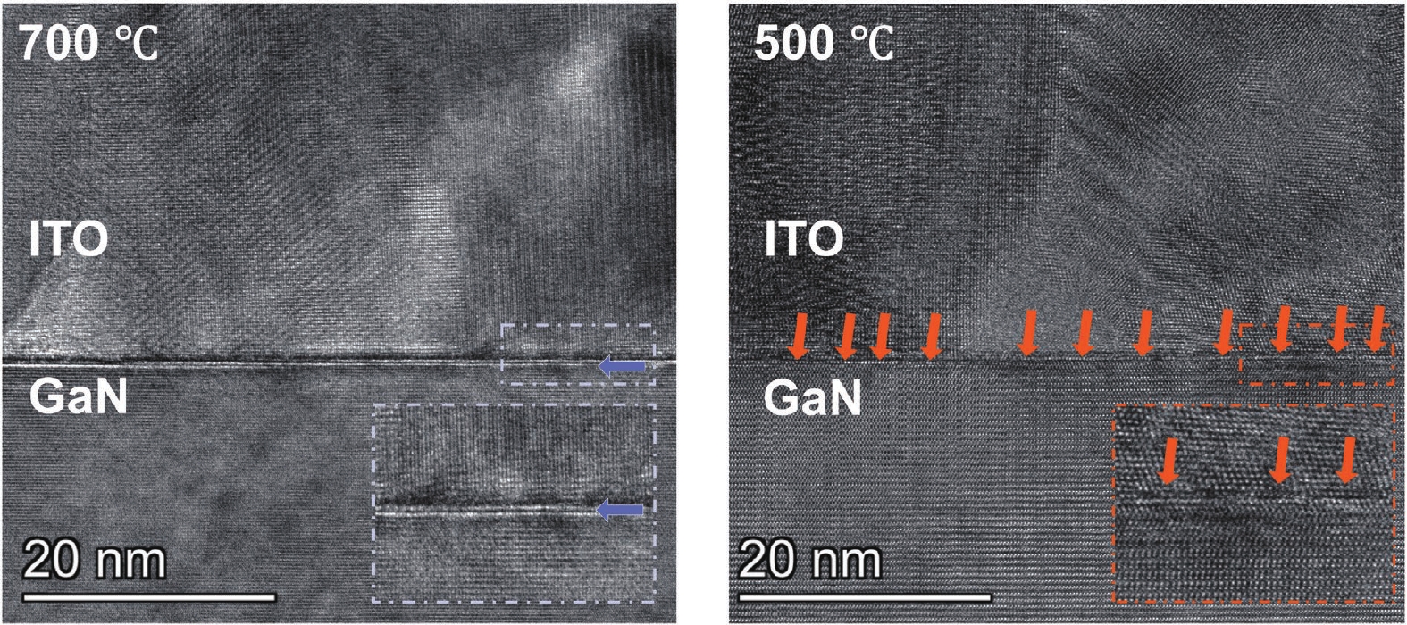
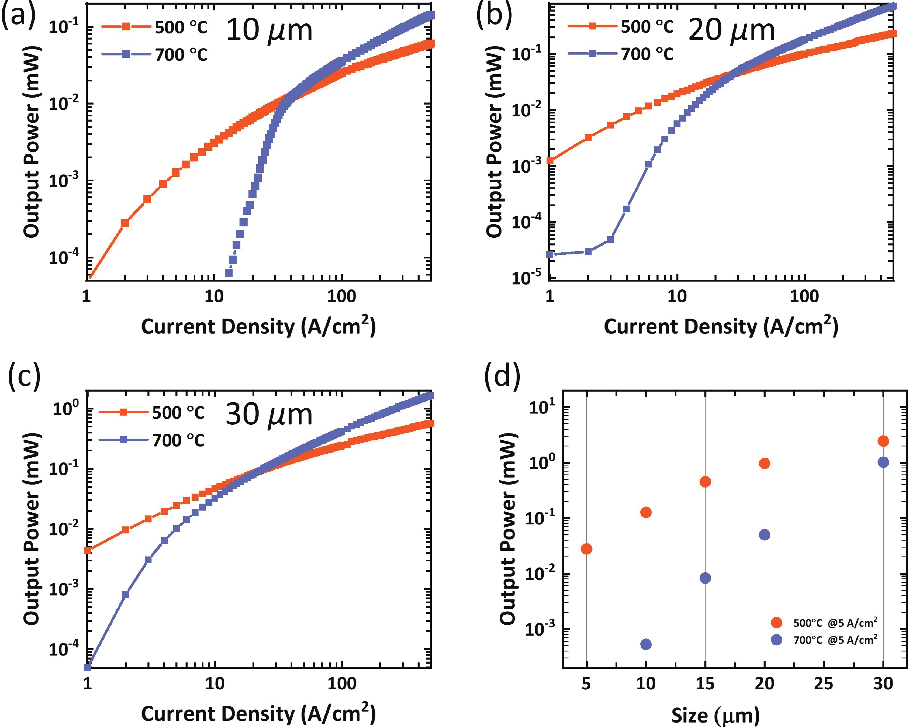
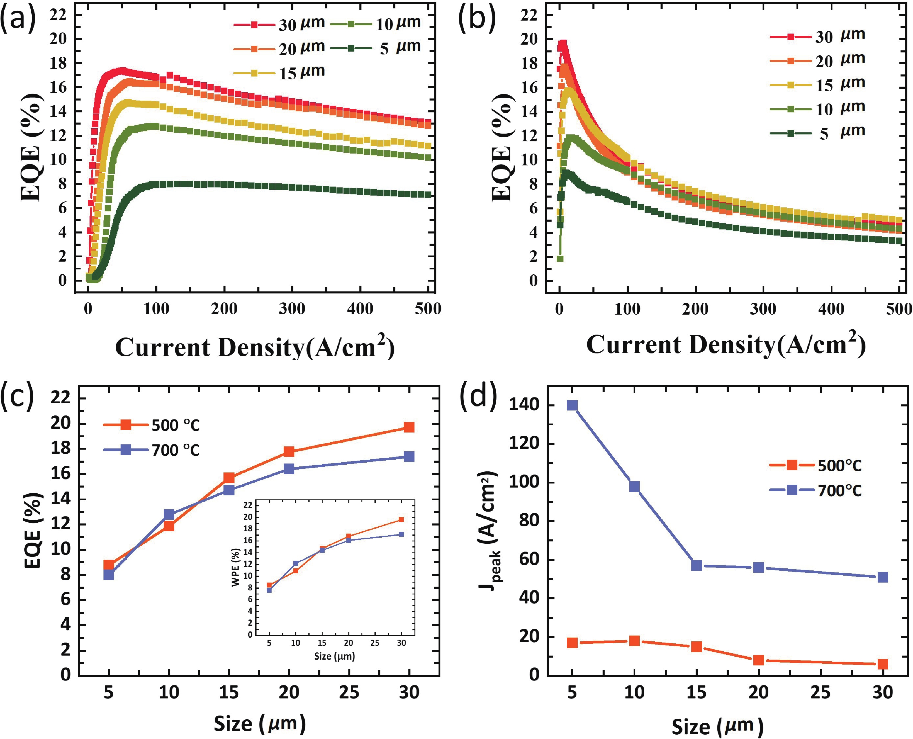
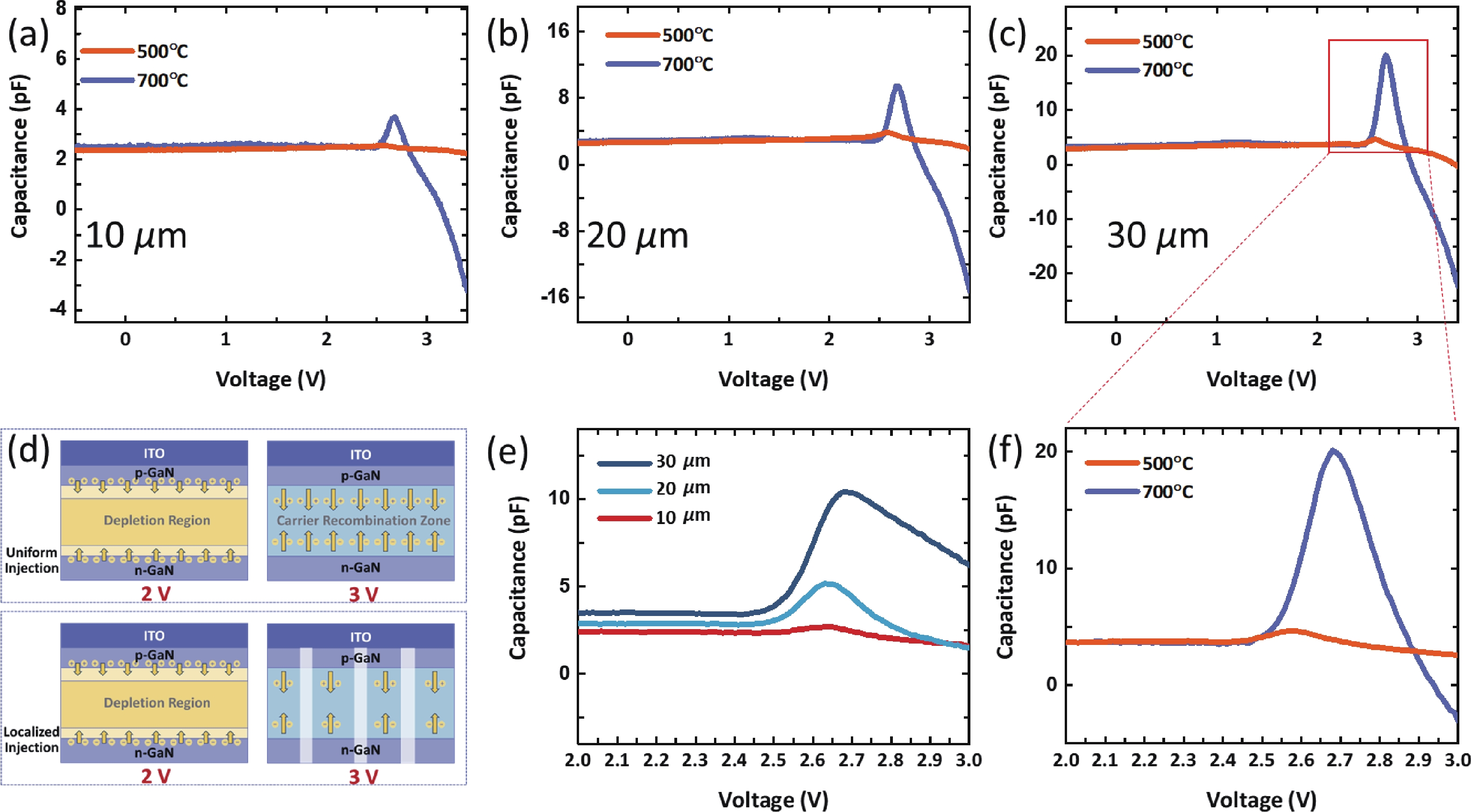
Abstract: Achieving high emission efficiency at low current densities remains a challenge for micro-LEDs. Here, we demonstrate a controllable interfacial strategy by tuning the annealing temperature of RF-superimposed DC sputtered ITO to modulate carrier injection dynamics. STEM analysis reveals 500 °C annealing triggers discrete substitutional In-atom incorporation into the p-GaN lattice, forming localized nanoscale contact regions. This architecture induces a localized carrier injection mechanism that significantly enhances the efficiency of micro-LEDs at low current densities. Specifically, the 500 °C-annealed 10 μm devices exhibit a dramatic enhancement in light output power (LOP), reaching 1.3 × 10⁻¹ mW at 5 A/cm2, which is significantly higher than the 5.3 × 10⁻⁴ mW measured for 700 °C-annealed devices. Furthermore, the peak efficiency current density (Jpeak) is dramatically shifted from 140 to 17 A/cm2 for 5 μm devices. Capacitance-voltage analysis further corroborates the localized carrier injection mechanism. These findings establish contact interfacial modulation as a robust strategy for optimizing micro-LEDs in low-power display applications and tailoring device-level performance across broader optoelectronics.

Key words: micro-LEDsgallium nitrideindium tin oxidelocalized contactrapid annealing


[1]
Guo W J, He W J, Qi Z W, et al. Research progresses on epitaxy and sidewall treatment for micro-LEDs. Prog Quantum Electronics, 2025, 104: 100598 doi: 10.1016/j.pquantelec.2025.100598
[2]
Jin Z X, Ying H, Zhang Z, et al. Toward 20-Gbps Single-Chip Space Division Multiplexing Visible Light Communication Based on a Low-Crosstalk Micro-LED Array. J Lightwave Technol, 2025(24): 10960 doi: 10.1109/jlt.2025.3620260
[3]
Zhu S J, Shan X Y, Lin R Z, et al. Characteristics of GaN-on-Si Green Micro-LED for Wide Color Gamut Display and High-Speed Visible Light Communication. ACS Photonics, 2022, 10: 92
[4]
Yu L M, Wang L, Hao Z B, et al. High-speed micro-LEDs for visible light communication: challenges and progresses. Semicond Sci Technol, 2022, 37(2): 023001 doi: 10.1088/1361-6641/ac40ec
[5]
Lu S Q, Li J C, Huang K, et al. Designs of InGaN Micro-LED Structure for Improving Quantum Efficiency at Low Current Density. Nanoscale Res Lett, 2021, 16(1): 99 doi: 10.1186/s11671-021-03557-4
[6]
Hung W C, Chang S P, Chang S J, et al. Exploring an InGaN Micro-LED structure for optimum IQE operating on low current condition through simulation study. International J Mod Phys B, 2025, 39(06): 2540029 doi: 10.1142/S0217979225400296
[7]
Wang A M, Chen K X, Kang J. High external quantum efficiency in InGaN-based green micro-light emitting diodes at ultra-low current density by removing pre-wells. Appl Phys Express, 2025, 18(1): 011001 doi: 10.35848/1882-0786/ada689
[8]
Wei A C, Wang S H, Sze J R, Pham Q H. Improvement of the Internal Quantum Efficiency of III-Nitride Blue Micro-Light-Emitting Diodes by the Hole Accelerator at the Low Current Density. Adv Photonics Res, 2024, 5(9): 2300262 doi: 10.1002/adpr.202300262
[9]
Zheng L, Cai S, Chen G, et al. Impacts of removing the p-AlGaN electron blocking layer for ultra-low-current injected blue micro-LEDs. Opt Express, 2025, 33(4): 8536 doi: 10.1364/OE.549908
[10]
Xing K, Wang H F, Lin L Y, et al. Impact of Template Patterning Dimensions on the Performance of InGaN-Based Red Light-Emitting Diodes. IEEE Trans Electron Devices, 2025, 72(1): 394
[11]
Hang S, He S Q, Yang Z H, et al. Stepwise gradient etching for low-defect GaN Micro-LEDs with suppressed non-radiative recombination. Opt Lett, 2025, 50(22): 7155 doi: 10.1364/OL.578029
[12]
Chu E K, Youn E J, Kim H W, et al. Wafer-Scale Characterization of 1692-Pixel-Per-Inch Blue Micro-LED Arrays with an Optimized ITO Layer. Micromachines, 2024, 15(5): 560 doi: 10.3390/mi15050560
[13]
Zahir N, Talik N A, Harun H N, et al. Improved performance of InGaN/GaN LED by optimizing the properties of the bulk and interface of ITO on p-GaN. Appl Surf Sci, 2021, 540: 148406 doi: 10.1016/j.apsusc.2020.148406
[14]
Cho W S, Park J Y, Yoo C J, Lee J L. Design of highly transparent ohmic contact to N face n-GaN for enhancing light extraction in GaN-based micro LED display. Opt Express, 2023, 31(25): 41611 doi: 10.1364/OE.506700
[15]
Chang S J, Lan C H, Hwang J D, et al. Sputtered indium-tin-oxide on p-GaN. J Electrochem Soc, 2008, 155(2): H140 doi: 10.1149/1.2820626
[16]
Son K J, Kim T K, Cha Y J, et al. Impact of Plasma Electron Flux on Plasma Damage-Free Sputtering of Ultrathin Tin-Doped Indium Oxide Contact Layer on p-GaN for InGaN/GaN Light-Emitting Diodes. Adv Sci, 2018, 5(2): 1700637 doi: 10.1002/advs.201700637
[17]
Torii H, Matsui S. Characterization and ohmic contact properties of indium tin-oxide films prepared on p-type GaN using electron-cyclotron-resonance plasma-sputter deposition. Thin Solid Films, 2024, 803: 140464 doi: 10.1016/j.tsf.2024.140464
[18]
Deng C H, Chen Z Z, Dong B Y, et al. Strongly Localized Excitons for Efficient Micro-Light-Emitting-Diodes under Low Injection Levels. ACS Appl Electron Mater, 2025, 7(9): 4220 doi: 10.1021/acsaelm.5c00396
[19]
Liu Z Y, Cao H C, Tang X, et al. Advanced technologies in InGaN micro-LED fabrication to mitigate the sidewall effect. Light Sci Appl, 2025, 14(1): 64 doi: 10.1038/s41377-025-01751-y
[20]
Liu Y B, Zhanghu M, Feng F, et al. Identifying the role of carrier overflow and injection current efficiency in a GaN-based micro-LED efficiency droop model. Opt Express, 2023, 31(11): 17557 doi: 10.1364/OE.487475
[21]
Yang W, Zhang S L, McKendry J J D, et al. Size-dependent capacitance study on InGaN-based micro-light-emitting diodes. J Appl Phys, 2014, 116(4): 044512 doi: 10.1063/1.4891233
[22]
Ershov M, Liu H C, Li L, et al. Negative capacitance effect in semiconductor devices. IEEE Trans on Electron Devices, 1998, 45(10): 2196 doi: 10.1109/16.725254
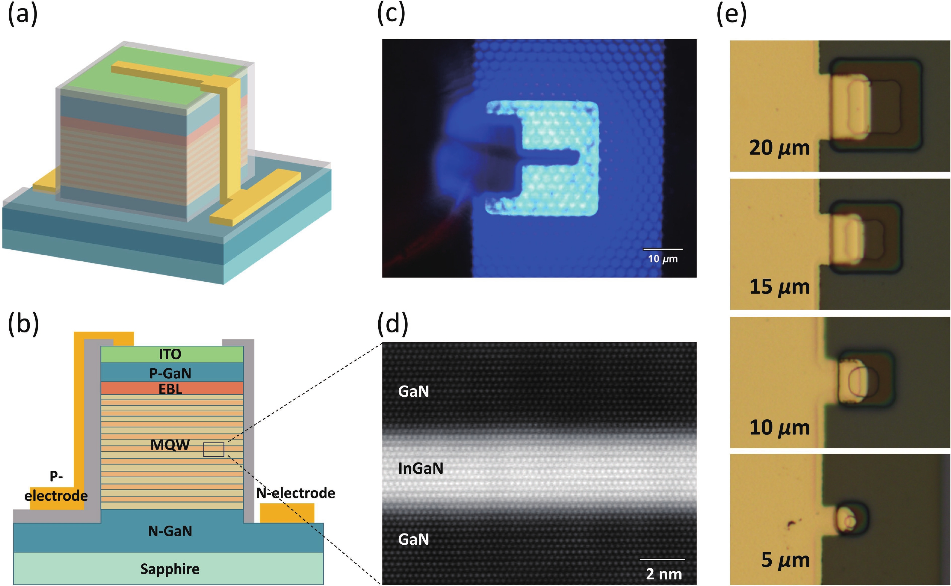
Fig. 1.  (Color online) (a) Schematic diagram of the micro-LED structure; (b) Schematic cross-section view of the micro-LED structure; (c) Optical micrograph of a 30 μm micro-LED pixel under current injection; (d) Cross-sectional STEM image focusing on the InGaN/GaN MQW region; (e) Optical microscope images of 20 to 5 µm Micro-LEDs.

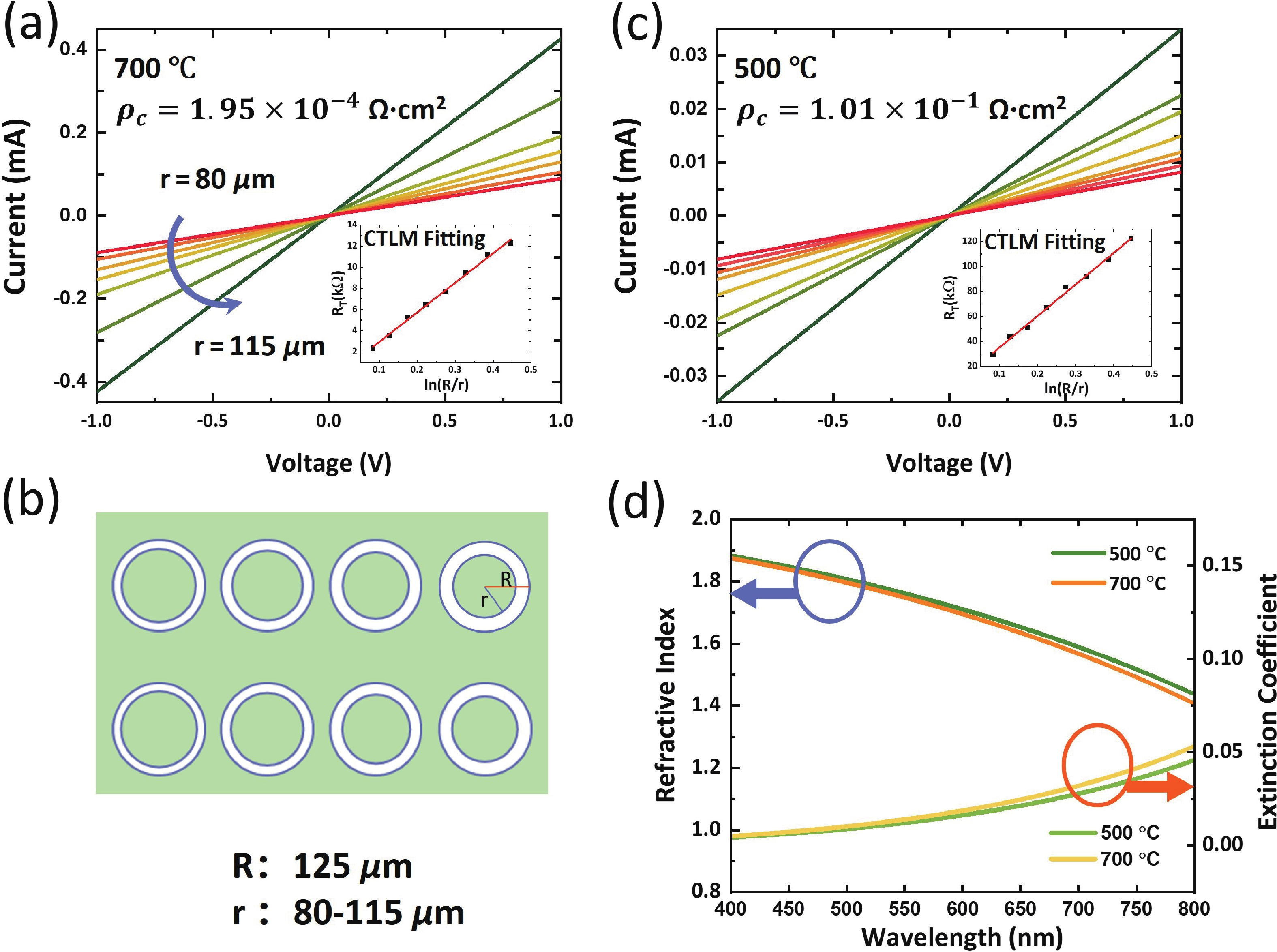
Fig. 2.  (Color online) (a) Schematic diagram of the CTLM patterns; I-V characteristics of the CTLM structures for the samples annealed at (b) 700 and (c) 500 °C; (d) refractive index (n) and extinction coefficient (k) of the ITO films annealed at 500 and 700 °C in the visible light range.

Fig. 3.  (Color online) STEM image of ITO/p-GaN interface

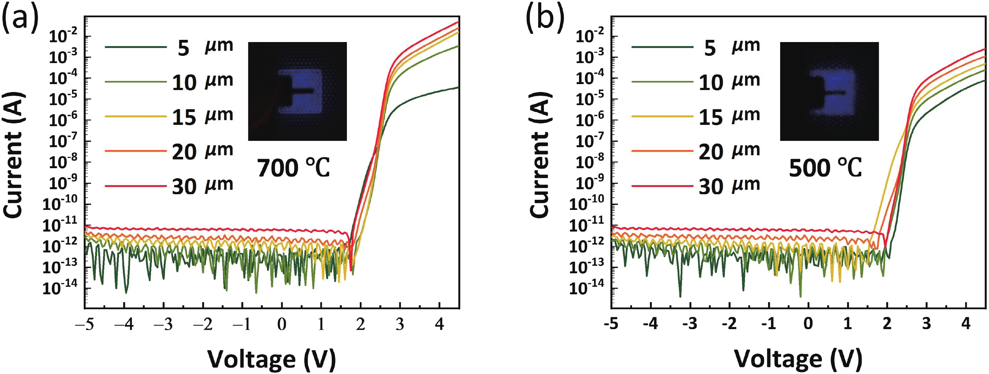
Fig. 4.  (Color online) Semi-logarithmic I-V curves of micro-LEDs with various sizes annealed at (a) 700 and (b) 500 °C.

Fig. 5.  (Color online) (a)-(c) Output power as a function of current density curves for devices with side-length of (a) 10, (b) 20 and (c) 30 µm; (d) Output power of micro-LEDs with different sizes measured at 5 A/cm2.

Fig. 6.  (Color online) EQE as a function of current density curves for micro-LEDs annealed at (a) 700 and (b) 500 °C; (c) Peak EQE and WPE for micro-LEDs of various sizes; (d) Jpeak of micro-LEDs with different sizes.

Fig. 7.  (Color online) (a)-(c) C-V characteristics for micro-LEDs with mesa sizes of 10, 20 and 30 µm; (d) Schematic illustration of the carrier injection distribution for uniform injection devices and localized injection devices; (e) Size-dependent C-V curves for the 700 °C sample; (f) Magnified view of the C-V curves for the 500 °C sample from (c).

[1]
Guo W J, He W J, Qi Z W, et al. Research progresses on epitaxy and sidewall treatment for micro-LEDs. Prog Quantum Electronics, 2025, 104: 100598 doi: 10.1016/j.pquantelec.2025.100598
[2]
Jin Z X, Ying H, Zhang Z, et al. Toward 20-Gbps Single-Chip Space Division Multiplexing Visible Light Communication Based on a Low-Crosstalk Micro-LED Array. J Lightwave Technol, 2025(24): 10960 doi: 10.1109/jlt.2025.3620260
[3]
Zhu S J, Shan X Y, Lin R Z, et al. Characteristics of GaN-on-Si Green Micro-LED for Wide Color Gamut Display and High-Speed Visible Light Communication. ACS Photonics, 2022, 10: 92
[4]
Yu L M, Wang L, Hao Z B, et al. High-speed micro-LEDs for visible light communication: challenges and progresses. Semicond Sci Technol, 2022, 37(2): 023001 doi: 10.1088/1361-6641/ac40ec
[5]
Lu S Q, Li J C, Huang K, et al. Designs of InGaN Micro-LED Structure for Improving Quantum Efficiency at Low Current Density. Nanoscale Res Lett, 2021, 16(1): 99 doi: 10.1186/s11671-021-03557-4
[6]
Hung W C, Chang S P, Chang S J, et al. Exploring an InGaN Micro-LED structure for optimum IQE operating on low current condition through simulation study. International J Mod Phys B, 2025, 39(06): 2540029 doi: 10.1142/S0217979225400296
[7]
Wang A M, Chen K X, Kang J. High external quantum efficiency in InGaN-based green micro-light emitting diodes at ultra-low current density by removing pre-wells. Appl Phys Express, 2025, 18(1): 011001 doi: 10.35848/1882-0786/ada689
[8]
Wei A C, Wang S H, Sze J R, Pham Q H. Improvement of the Internal Quantum Efficiency of III-Nitride Blue Micro-Light-Emitting Diodes by the Hole Accelerator at the Low Current Density. Adv Photonics Res, 2024, 5(9): 2300262 doi: 10.1002/adpr.202300262
[9]
Zheng L, Cai S, Chen G, et al. Impacts of removing the p-AlGaN electron blocking layer for ultra-low-current injected blue micro-LEDs. Opt Express, 2025, 33(4): 8536 doi: 10.1364/OE.549908
[10]
Xing K, Wang H F, Lin L Y, et al. Impact of Template Patterning Dimensions on the Performance of InGaN-Based Red Light-Emitting Diodes. IEEE Trans Electron Devices, 2025, 72(1): 394
[11]
Hang S, He S Q, Yang Z H, et al. Stepwise gradient etching for low-defect GaN Micro-LEDs with suppressed non-radiative recombination. Opt Lett, 2025, 50(22): 7155 doi: 10.1364/OL.578029
[12]
Chu E K, Youn E J, Kim H W, et al. Wafer-Scale Characterization of 1692-Pixel-Per-Inch Blue Micro-LED Arrays with an Optimized ITO Layer. Micromachines, 2024, 15(5): 560 doi: 10.3390/mi15050560
[13]
Zahir N, Talik N A, Harun H N, et al. Improved performance of InGaN/GaN LED by optimizing the properties of the bulk and interface of ITO on p-GaN. Appl Surf Sci, 2021, 540: 148406 doi: 10.1016/j.apsusc.2020.148406
[14]
Cho W S, Park J Y, Yoo C J, Lee J L. Design of highly transparent ohmic contact to N face n-GaN for enhancing light extraction in GaN-based micro LED display. Opt Express, 2023, 31(25): 41611 doi: 10.1364/OE.506700
[15]
Chang S J, Lan C H, Hwang J D, et al. Sputtered indium-tin-oxide on p-GaN. J Electrochem Soc, 2008, 155(2): H140 doi: 10.1149/1.2820626
[16]
Son K J, Kim T K, Cha Y J, et al. Impact of Plasma Electron Flux on Plasma Damage-Free Sputtering of Ultrathin Tin-Doped Indium Oxide Contact Layer on p-GaN for InGaN/GaN Light-Emitting Diodes. Adv Sci, 2018, 5(2): 1700637 doi: 10.1002/advs.201700637
[17]
Torii H, Matsui S. Characterization and ohmic contact properties of indium tin-oxide films prepared on p-type GaN using electron-cyclotron-resonance plasma-sputter deposition. Thin Solid Films, 2024, 803: 140464 doi: 10.1016/j.tsf.2024.140464
[18]
Deng C H, Chen Z Z, Dong B Y, et al. Strongly Localized Excitons for Efficient Micro-Light-Emitting-Diodes under Low Injection Levels. ACS Appl Electron Mater, 2025, 7(9): 4220 doi: 10.1021/acsaelm.5c00396
[19]
Liu Z Y, Cao H C, Tang X, et al. Advanced technologies in InGaN micro-LED fabrication to mitigate the sidewall effect. Light Sci Appl, 2025, 14(1): 64 doi: 10.1038/s41377-025-01751-y
[20]
Liu Y B, Zhanghu M, Feng F, et al. Identifying the role of carrier overflow and injection current efficiency in a GaN-based micro-LED efficiency droop model. Opt Express, 2023, 31(11): 17557 doi: 10.1364/OE.487475
[21]
Yang W, Zhang S L, McKendry J J D, et al. Size-dependent capacitance study on InGaN-based micro-light-emitting diodes. J Appl Phys, 2014, 116(4): 044512 doi: 10.1063/1.4891233
[22]
Ershov M, Liu H C, Li L, et al. Negative capacitance effect in semiconductor devices. IEEE Trans on Electron Devices, 1998, 45(10): 2196 doi: 10.1109/16.725254
  • Search

    Advanced Search >>

    GET CITATION

    shu

    Export: BibTex EndNote

    Article Metrics

    Article views: 26 Times PDF downloads: 2 Times Cited by: 0 Times

    History

    Received: 19 March 2026 Revised: 24 April 2026 Online: Accepted Manuscript: 26 May 2026

    Catalog

      Email This Article

      User name:
      Email:*请输入正确邮箱
      Code:*验证码错误
      Ying Gu, Mengyang Huang, Jie Zhou, Zheyuan Hu, Peng Zhang, Min Jiang, Jianjun Zhu, Wenxian Yang, Shulong Lu. Annealing-modulated localized contact at ITO/p-GaN interface for high-efficiency micro-LEDs at low current density[J]. Journal of Semiconductors, 2026, In Press. doi: 10.1088/1674-4926/26030032 ****Y Gu, M Y Huang, J Zhou, Z Y Hu, P Zhang, M Jiang, J J Zhu, W X Yang, and S L Lu, Annealing-modulated localized contact at ITO/p-GaN interface for high-efficiency micro-LEDs at low current density[J]. J. Semicond., 2026, accepted doi: 10.1088/1674-4926/26030032
      Citation:
      Ying Gu, Mengyang Huang, Jie Zhou, Zheyuan Hu, Peng Zhang, Min Jiang, Jianjun Zhu, Wenxian Yang, Shulong Lu. Annealing-modulated localized contact at ITO/p-GaN interface for high-efficiency micro-LEDs at low current density[J]. Journal of Semiconductors, 2026, In Press. doi: 10.1088/1674-4926/26030032 ****
      Y Gu, M Y Huang, J Zhou, Z Y Hu, P Zhang, M Jiang, J J Zhu, W X Yang, and S L Lu, Annealing-modulated localized contact at ITO/p-GaN interface for high-efficiency micro-LEDs at low current density[J]. J. Semicond., 2026, accepted doi: 10.1088/1674-4926/26030032

      Annealing-modulated localized contact at ITO/p-GaN interface for high-efficiency micro-LEDs at low current density

      DOI: 10.1088/1674-4926/26030032
      CSTR: 32376.14.1674-4926.26030032
      More Information
      • Ying Gu received her B.S. degree from Suzhou University of technology. She is currently pursuing her Ph.D. degree at University of Science and Technology of China. Her research focuses on GaN-based micro-LEDs for visible light communication (VLC) and device performance optimization
      • Wenxian Yang received his Ph.D. degree from University of Science and Technology of China in 2019. He is currently an Associate Researcher and master’s supervisor at the Suzhou Institute of Nano-Tech and Nano-Bionics, Chinese Academy of Sciences. His research mainly focuses on the MBE growth of III-V compound semiconductor materials and GaN-based micro-LEDs
      • Shulong Lu received his Ph.D. degree from the Institute of Semiconductors, Chinese Academy of Sciences in 2003. He is currently a Researcher and Ph.D. supervisor at the Suzhou Institute of Nano-Tech and Nano-Bionics, Chinese Academy of Sciences. His research mainly focuses on the MBE growth of III-V compound semiconductor materials and related optoelectronic devices
      • Corresponding author: wxyang2014@sinano.ac.cnsllu2008@sinano.ac.cn
      • Received Date: 2026-03-19
      • Revised Date: 2026-04-24
      • Available Online: 2026-05-26

      Catalog

        /

        DownLoad:  Full-Size Img  PowerPoint
        Return
        Return