Issue Browser
Volume 47, Issue 7,
Jul 2026


J. Semicond.
2026, 47(7): 072101 doi: 10.1088/1674-4926/26020053
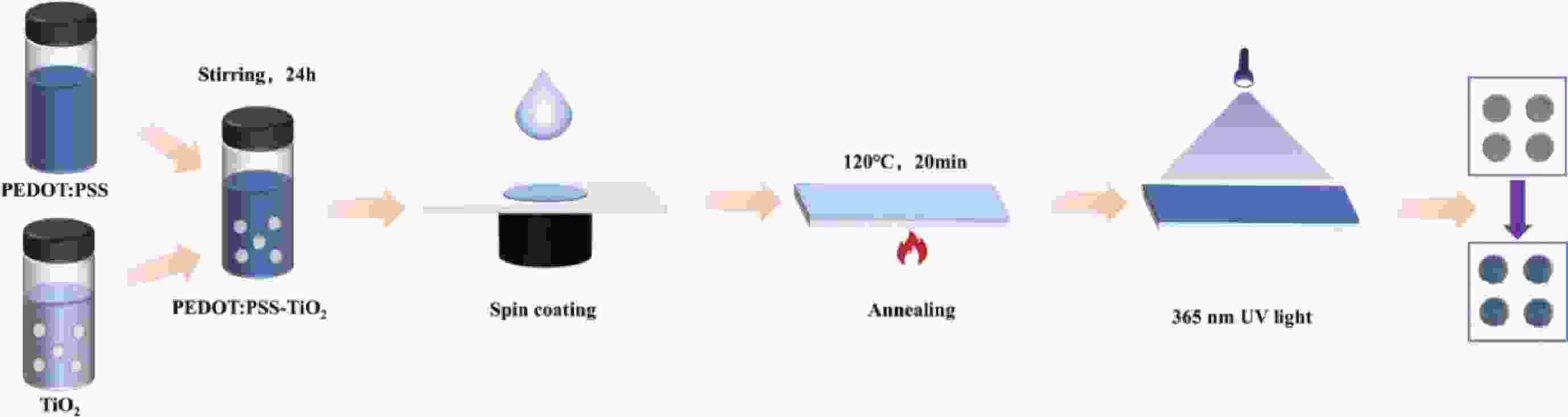
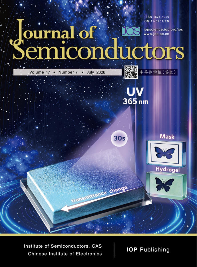
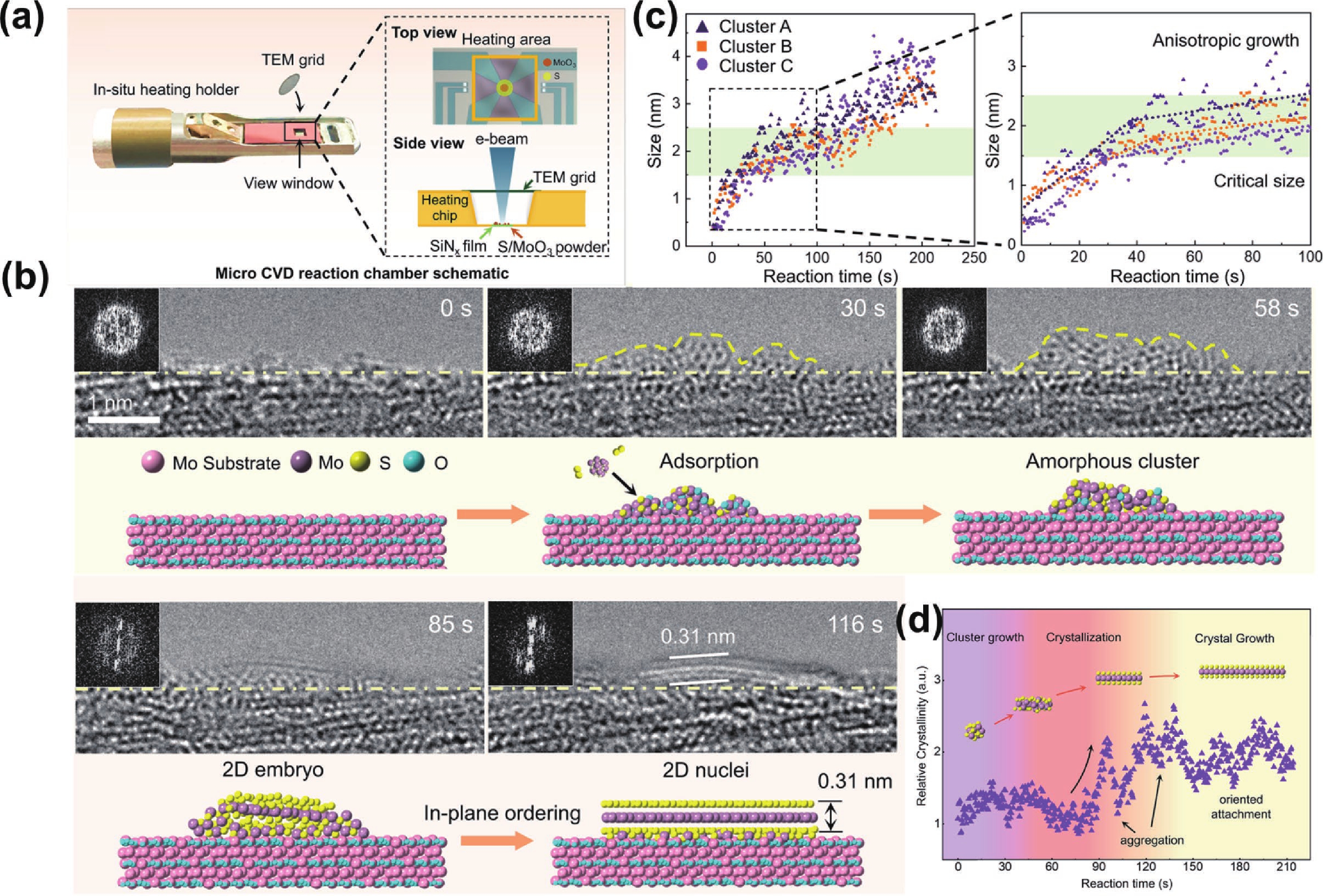
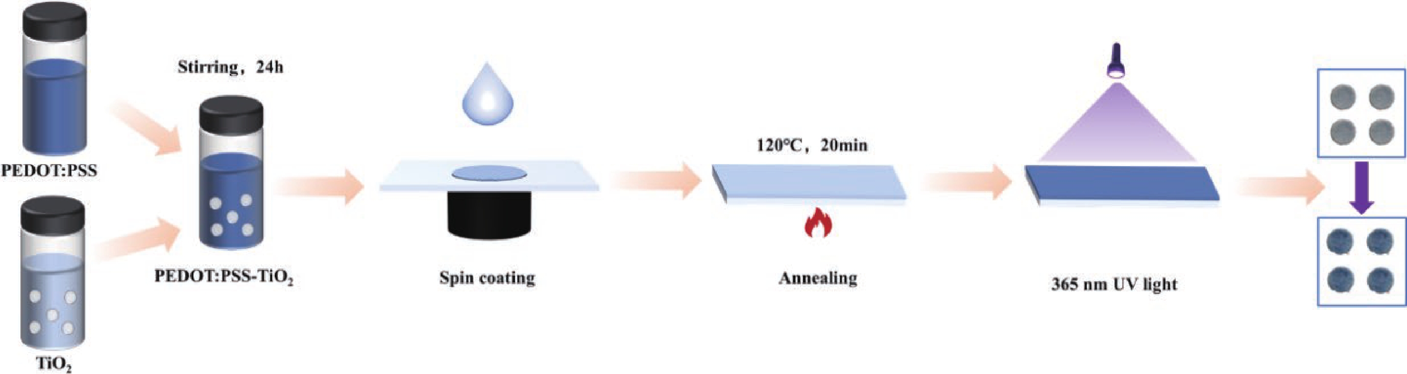
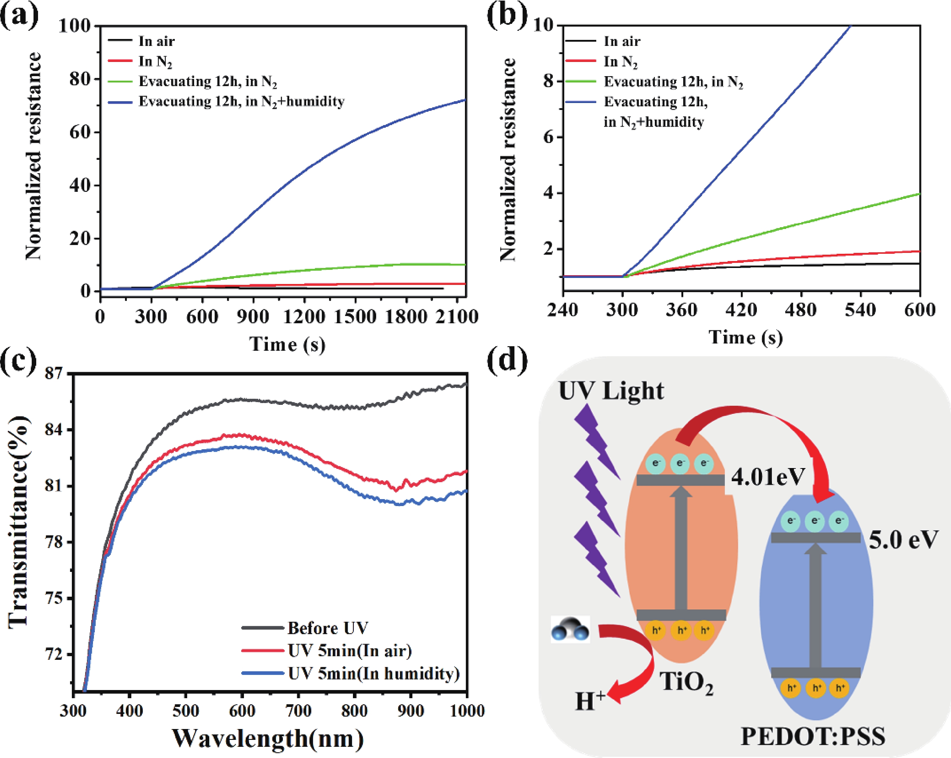
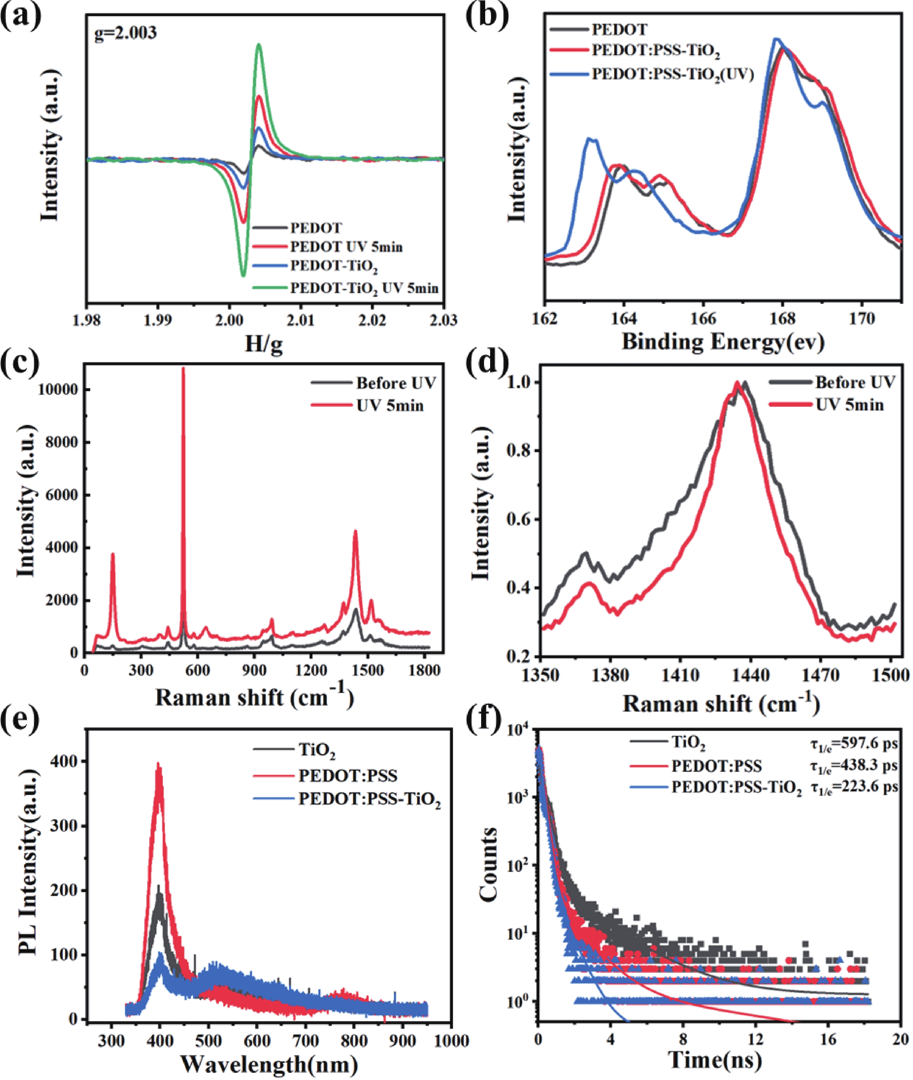
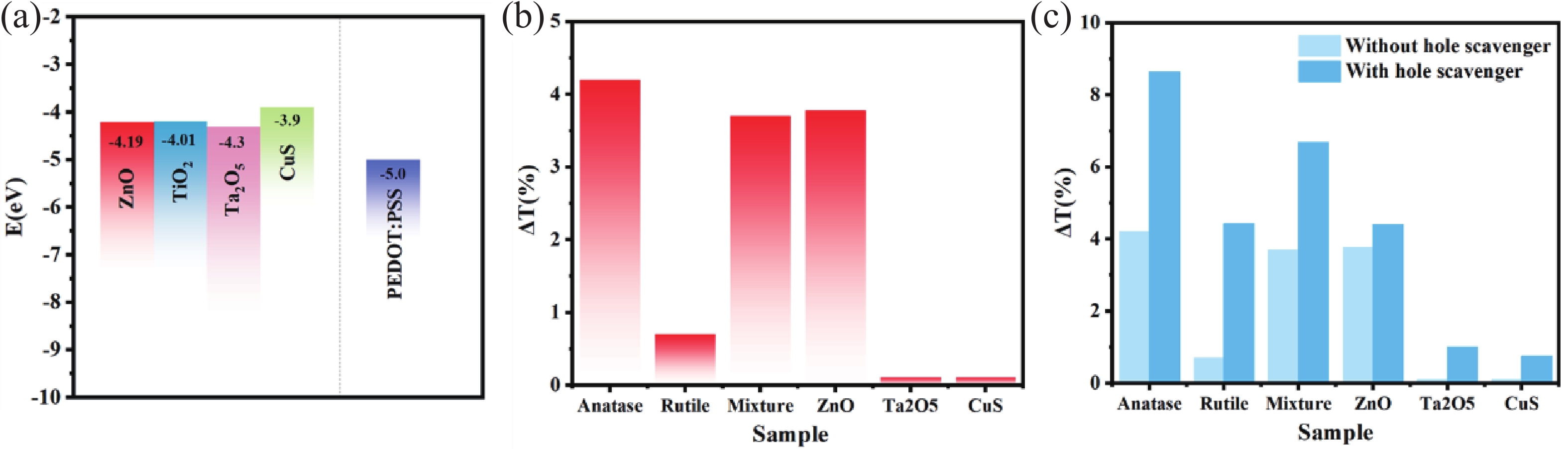
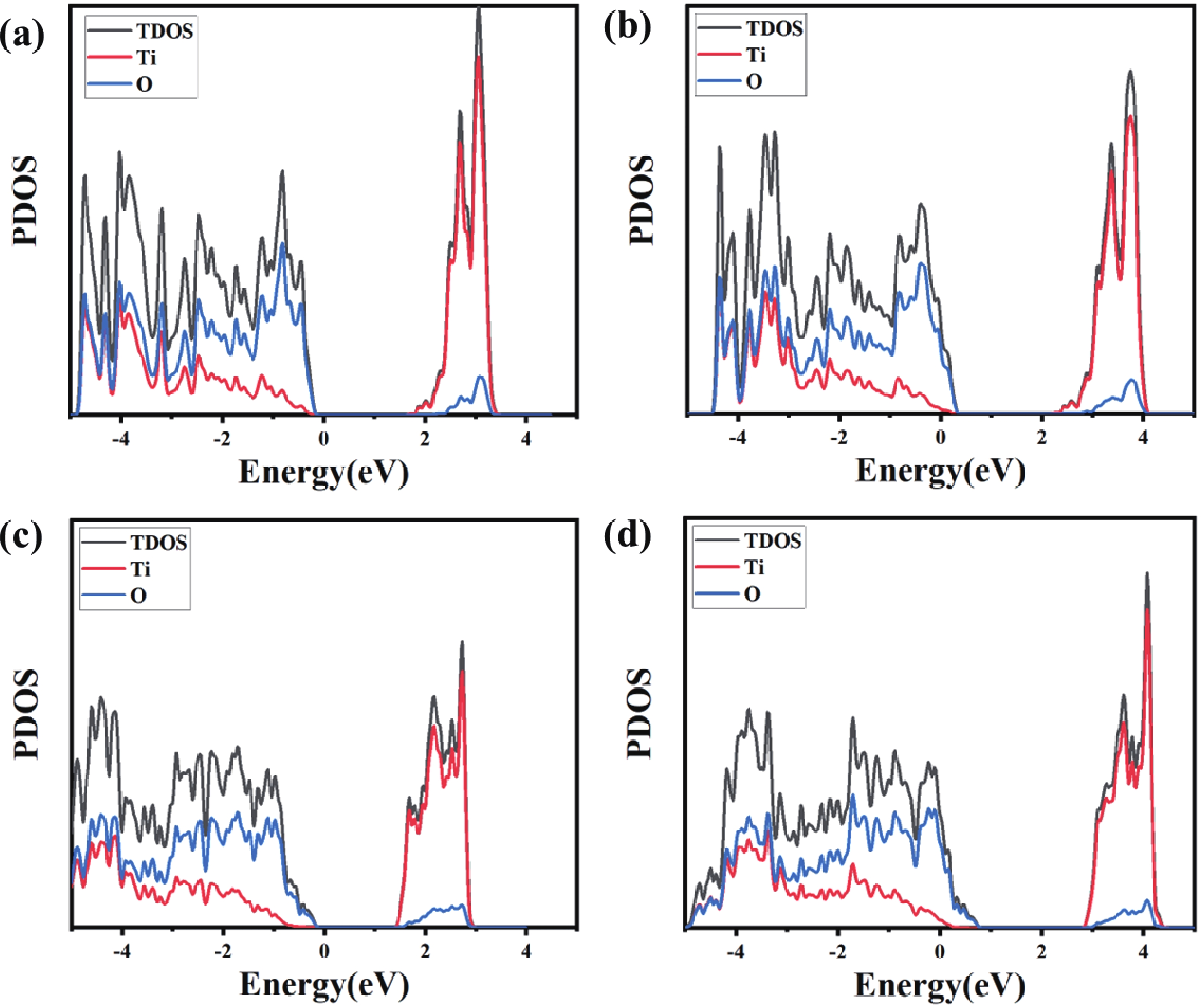
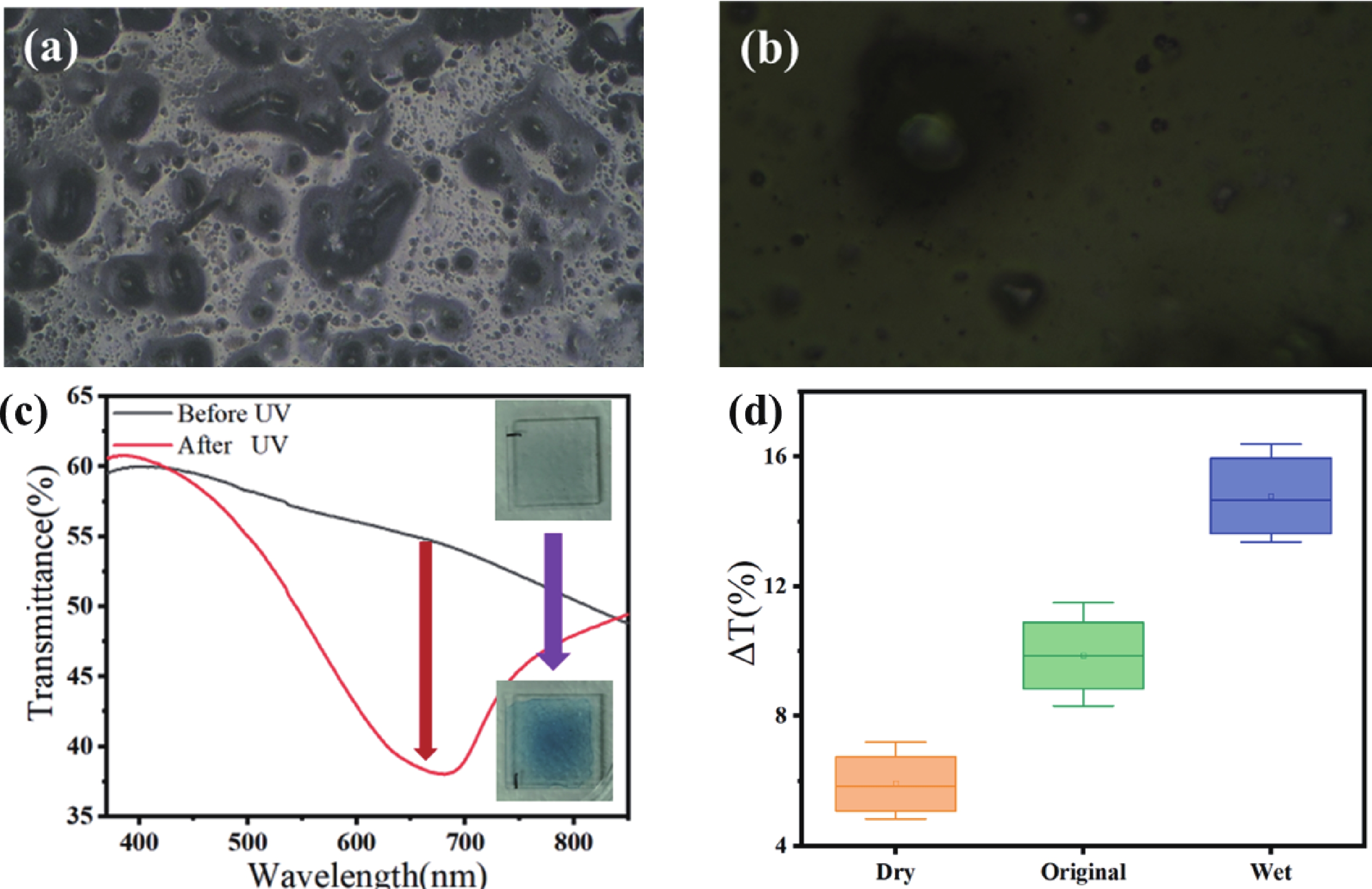
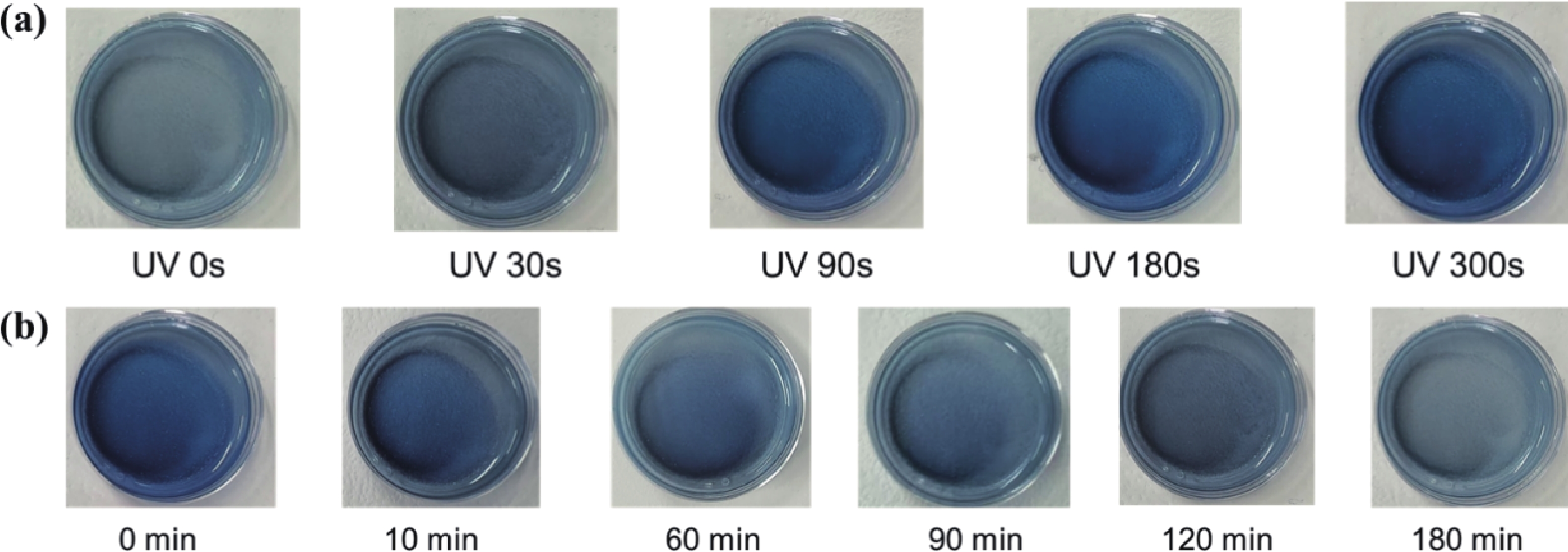
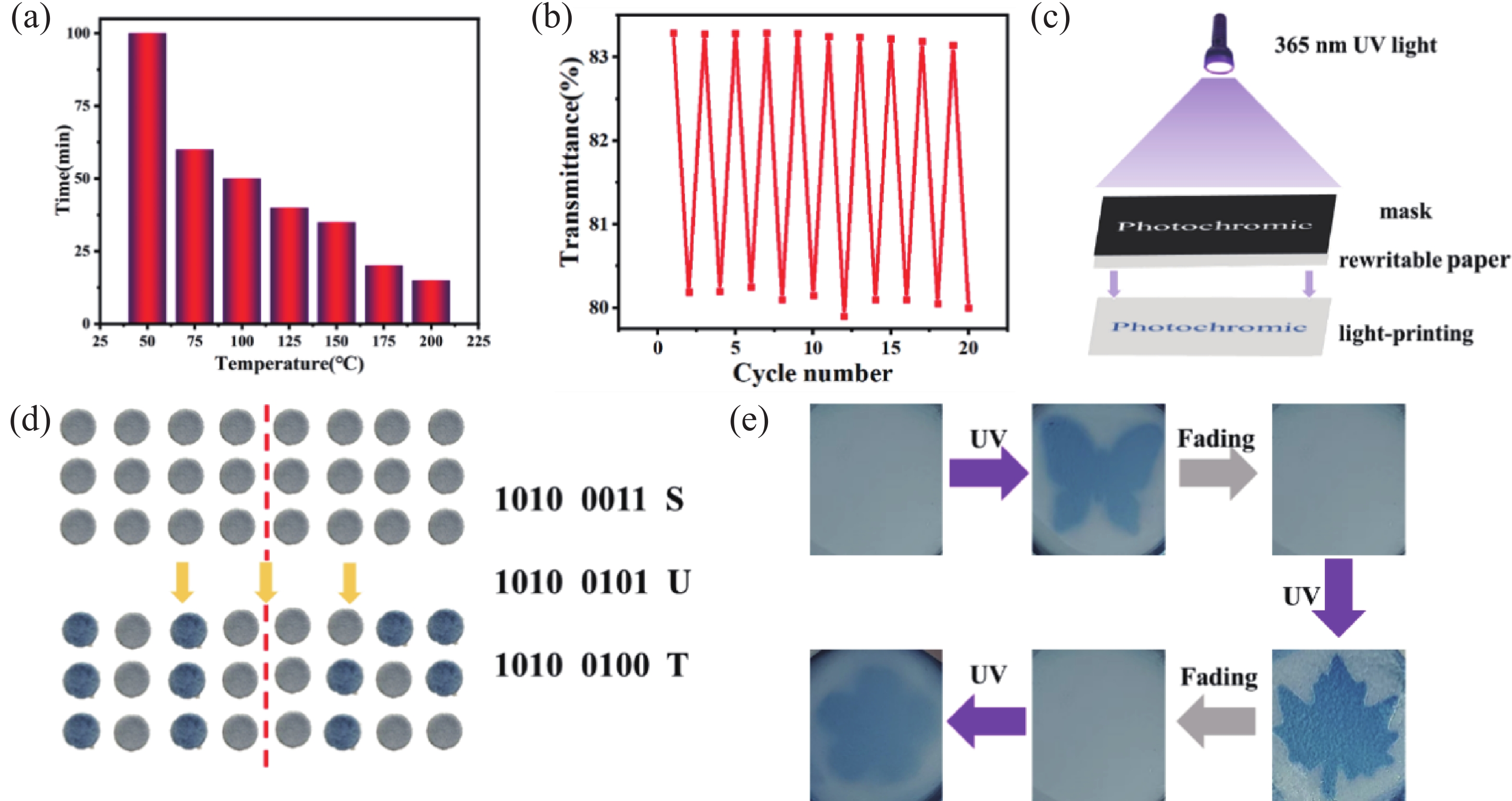
Integrating electrochromic (EC) and photochromic (PC) functions within a single material system holds great significance for the development of next-generation intelligent responsive materials. Traditional organic photochromic materials are all small molecules and oligomers, which require the photochemical response of specific photosensitive groups. However, PEDOT:PSS, a classic electrochromic polymer, has never been reported to exhibit photochromic properties due to the absence of photosensitive groups. Herein, we report for the first time the photochromic properties of PEDOT:PSS films, demonstrating their simultaneous capability of multi-field coupling response in the aspects of light, electricity and chemistry. The composite film undergoes a rapid color change from light blue to dark blue under ultraviolet light irradiation. This is attributed to the transformation process from the bipolarons state to the polarons state in the PEDOT:PSS, induced by photogenerated electrons as confirmed by EPR and Raman analyses. Furthermore, the developed hydrogel system enhances charge separation, yielding a 30.1% relative transmittance change and month-long stability. This work fills the long-standing gap in the understanding of the photochromic and electrochromic mechanisms of PEDOT:PSS, providing fundamental insights into carrier dynamics at organic−inorganic interfaces and laying the foundation for the development of multi-mode stimuli-responsive devices.
Interface engineering for high-efficiency spin injection and polarized emission in GaN-based devices
J. Semicond.
2026, 47(7): 072102 doi: 10.1088/1674-4926/25120016
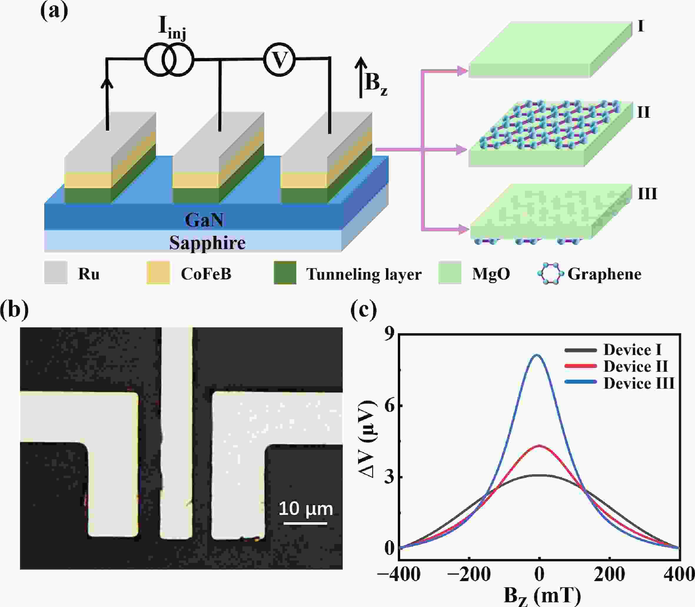
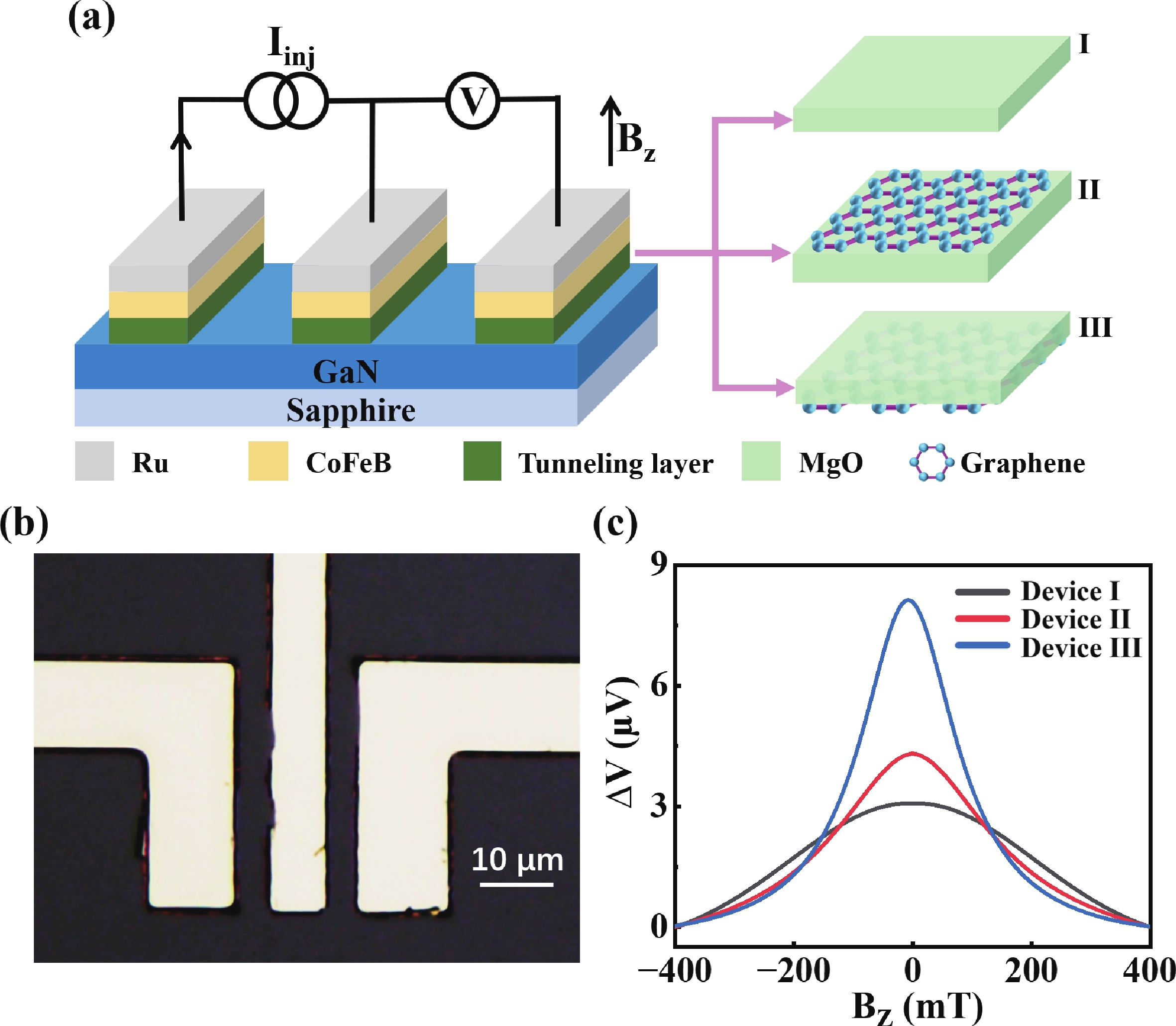
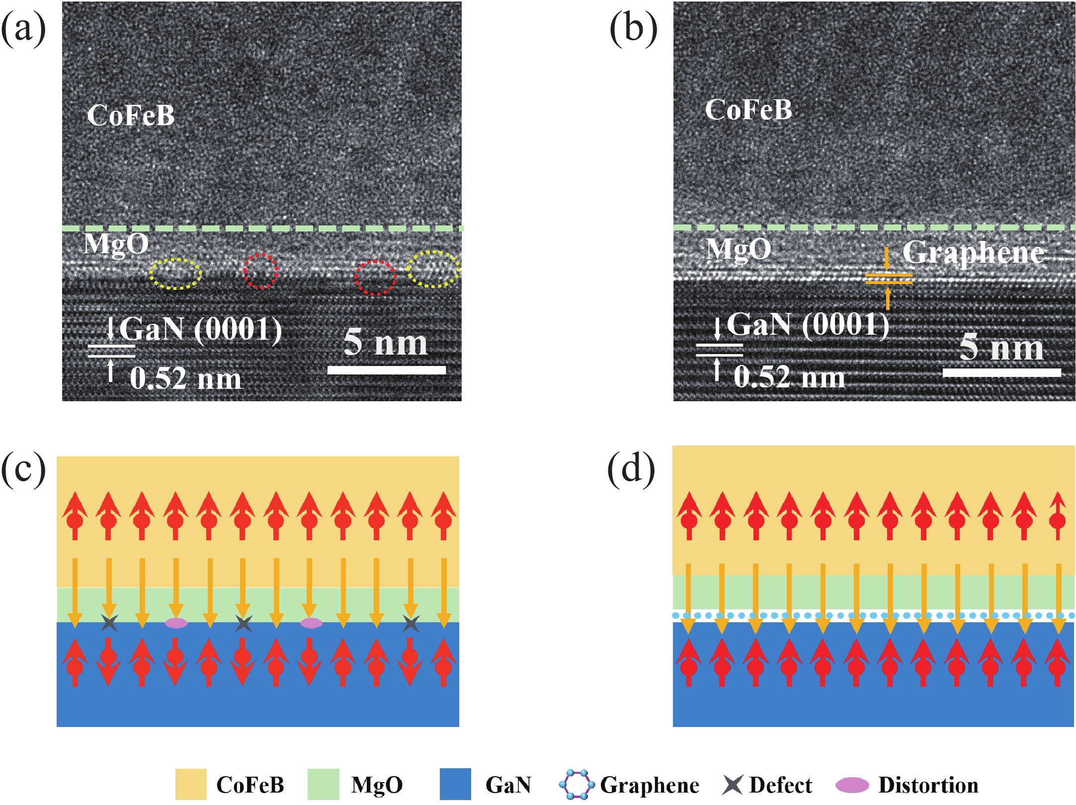
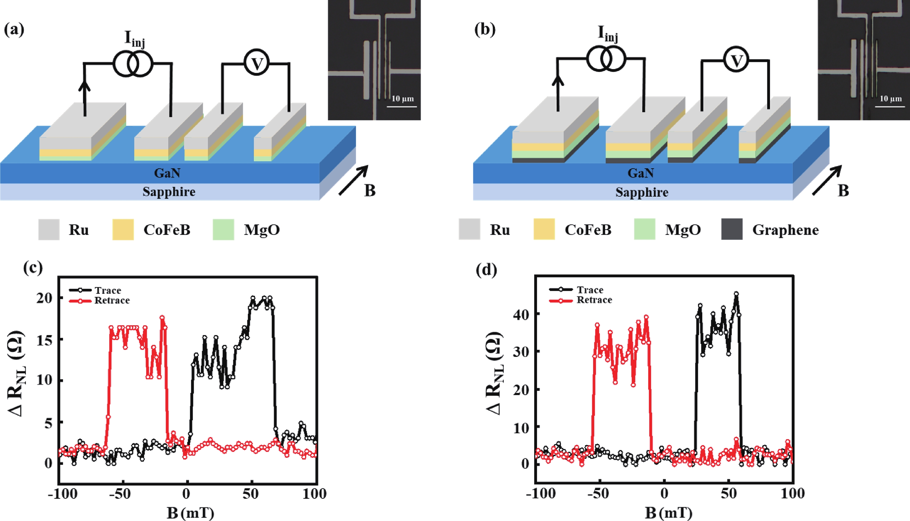
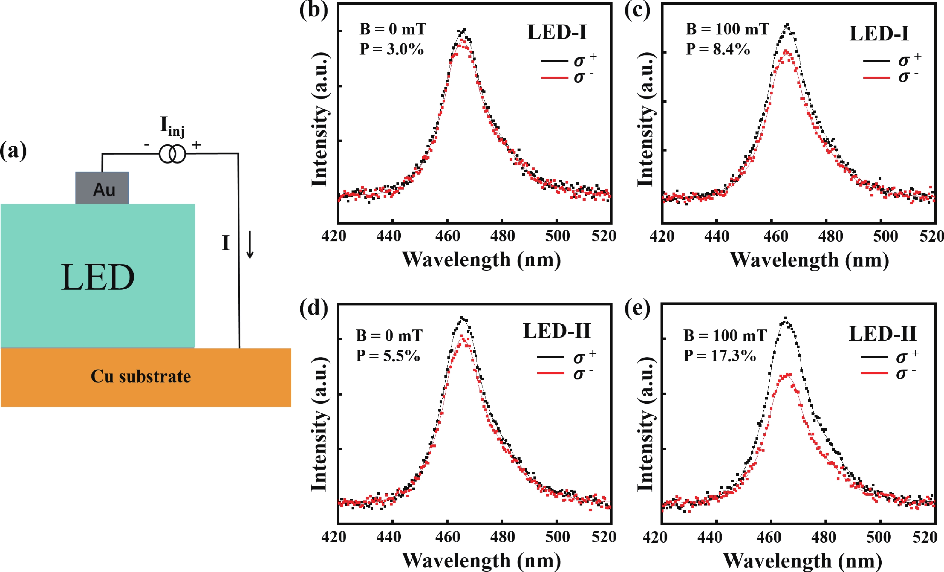
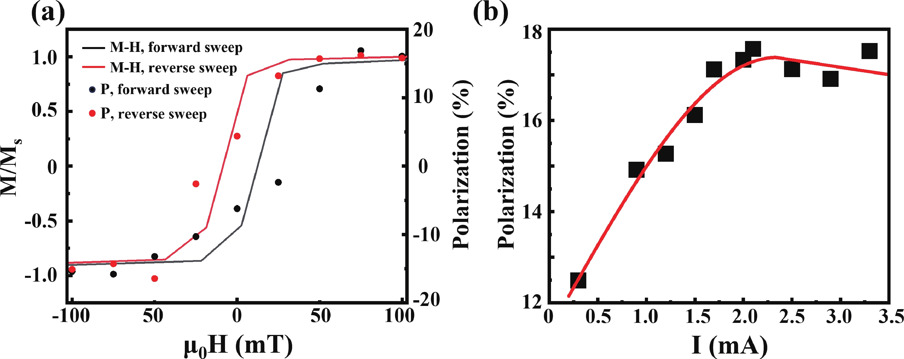
Efficient spin injection is crucial for developing high-performance spintronic and optoelectronic devices. To address the issue of low spin injection efficiency caused by lattice mismatch and interface defects in traditional CoFeB/MgO tunnel junctions, this work proposes a strategy of using graphene as an insertion layer to optimize interface quality and enhance the spin injection efficiency of tunnel junctions. By systematically investigating three types of tunnel junction structures, namely CoFeB/MgO, CoFeB/graphene/MgO, and CoFeB/MgO/graphene, we demonstrate that the graphene insertion layer can effectively release interface stress, reduce defects and distortions induced by lattice mismatch, and thereby suppress spin scattering. Meanwhile, it alleviates resistance mismatch while preserving high spin polarization. Ultimately, the spin injection polarization is increased from 10.6% to 16.2%, representing an enhancement of approximately 53%. Additionally, the optimized CoFeB/MgO/graphene tunnel junction was integrated into GaN-based spin light-emitting diodes, resulting in an increased circular polarization of electroluminescence from 8.4% to 17.3%. This work provides an interface engineering strategy for achieving efficient spin injection and advancing the development of spin-optoelectronic devices.
J. Semicond.
2026, 47(7): 072201 doi: 10.1088/1674-4926/26030004
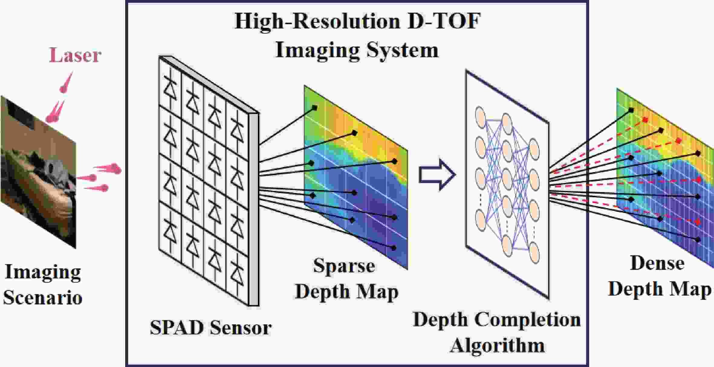
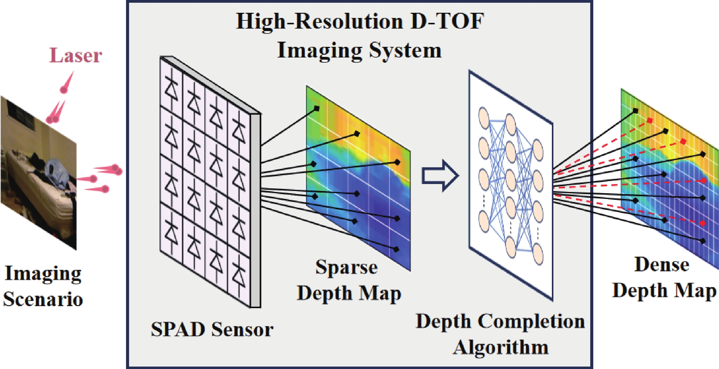
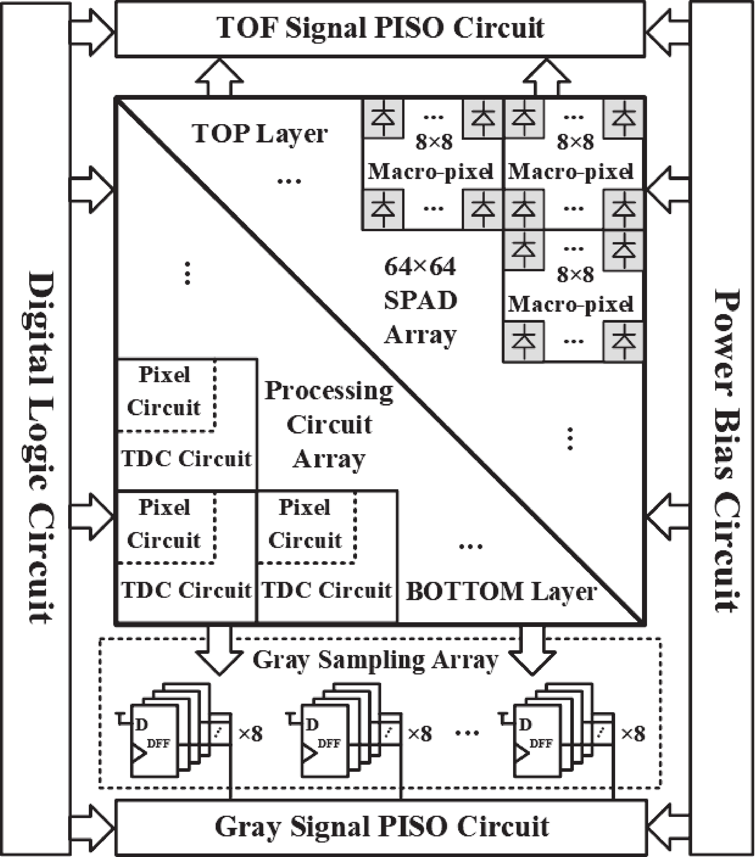
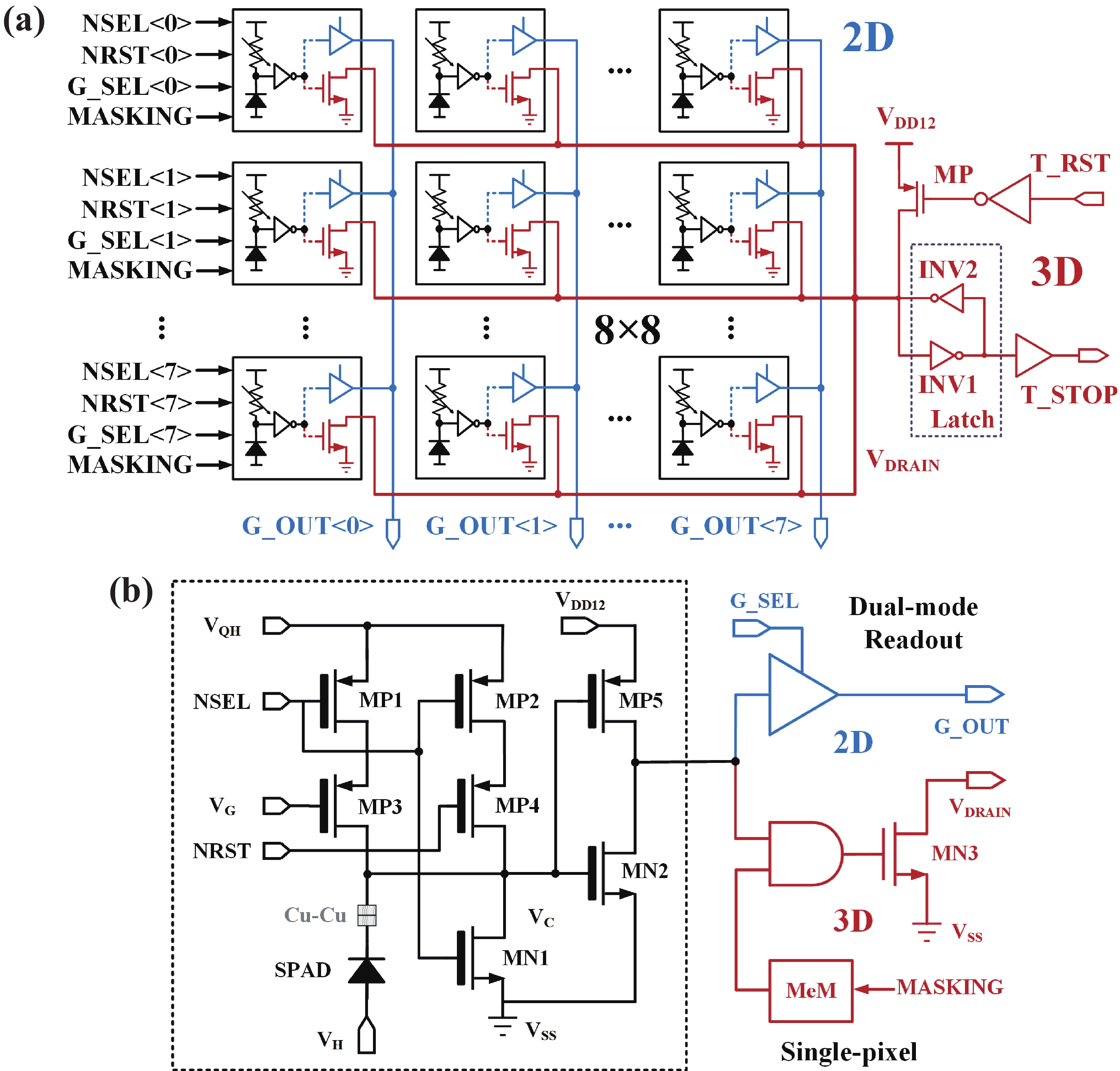
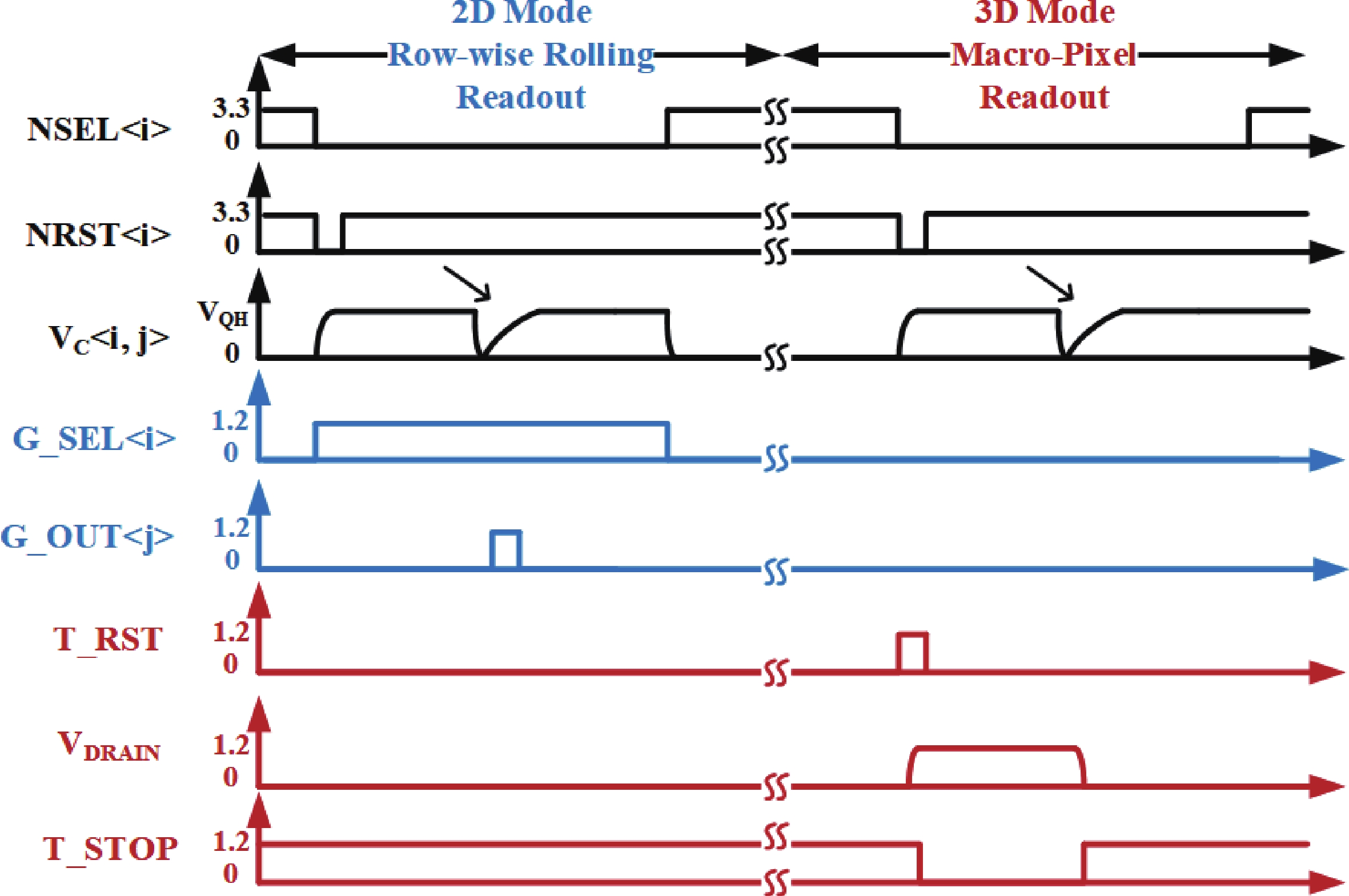
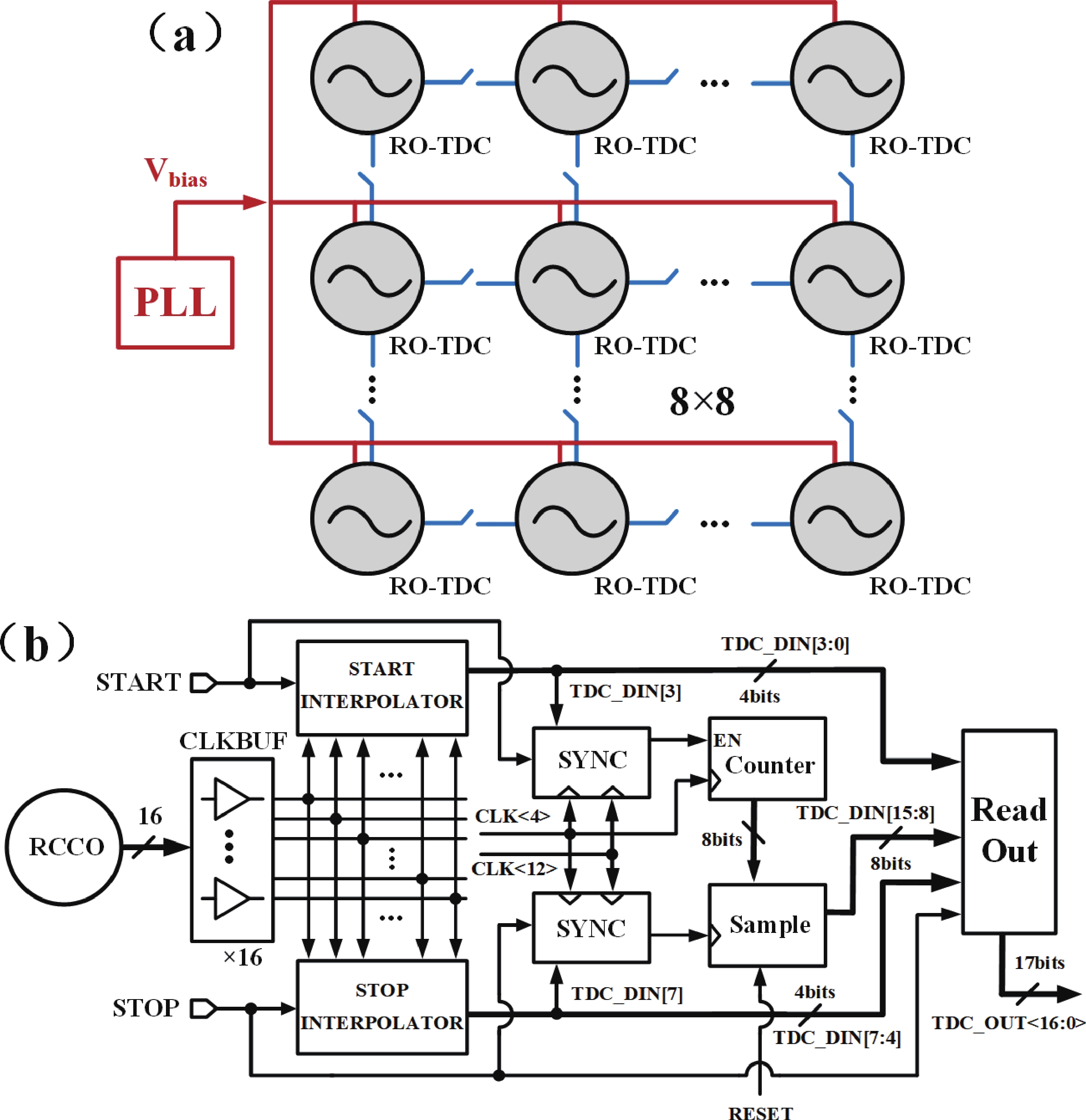
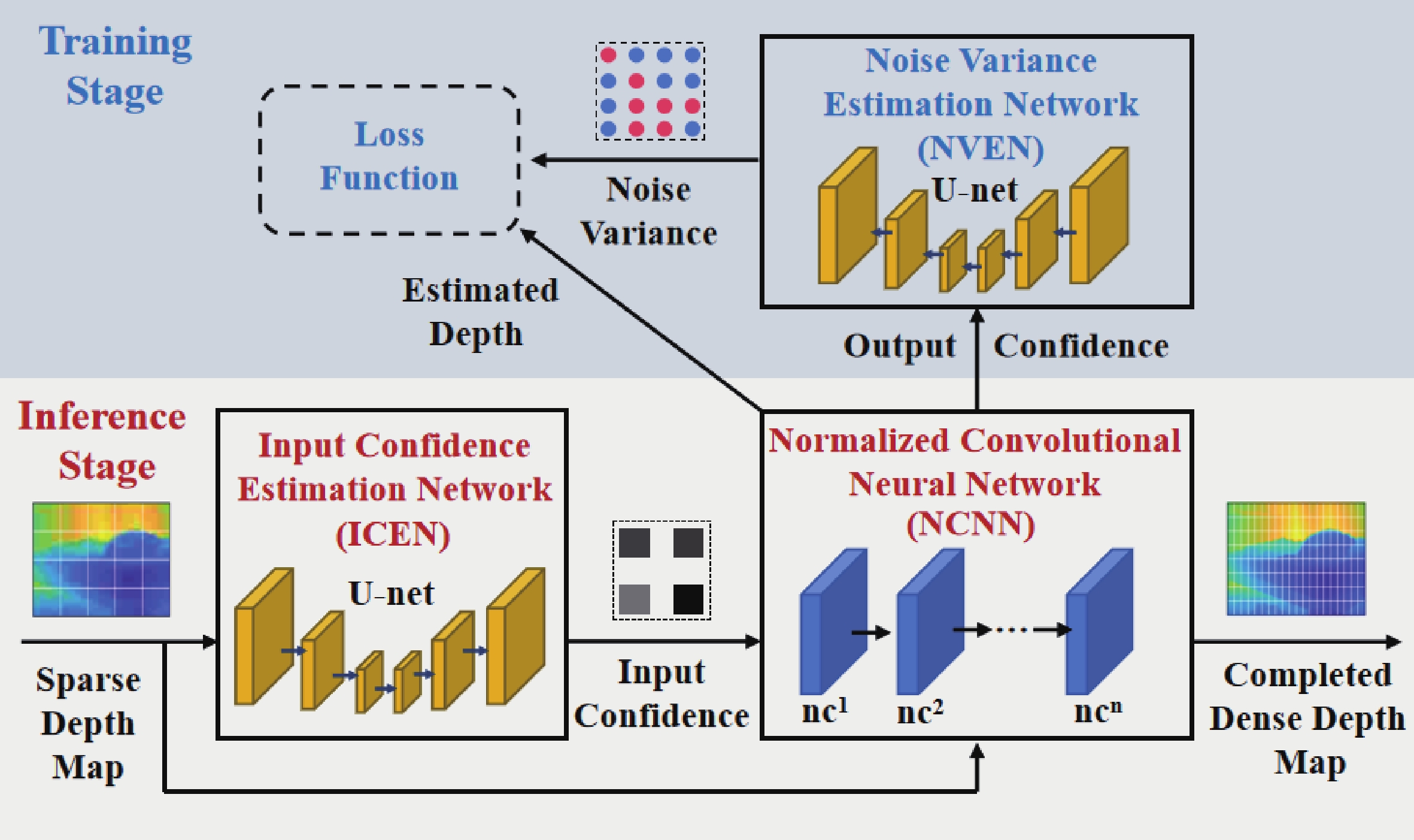
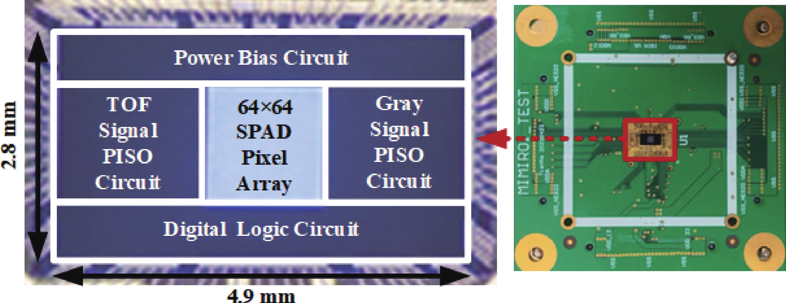
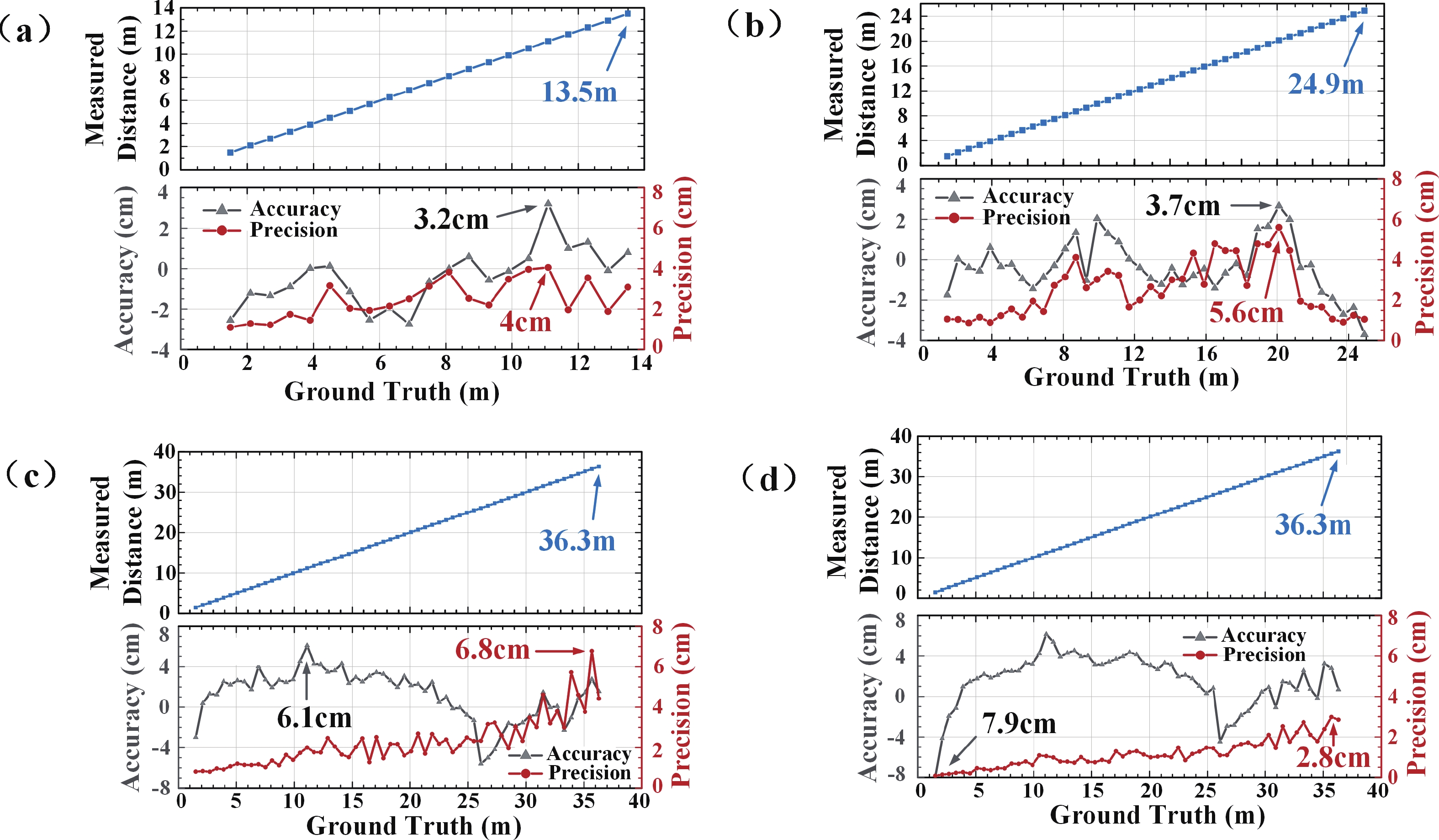
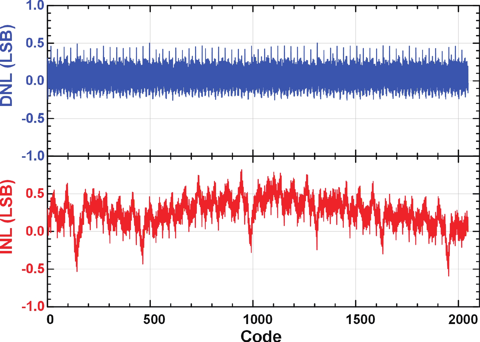
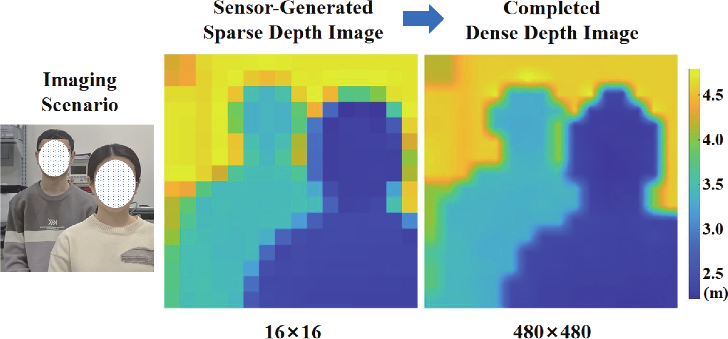
Single-photon avalanche diode (SPAD) image sensors are widely used in direct time-of-flight (D-TOF) imaging, but their ranging performance is often constrained by limited laser power. This article presents a SPAD-based D-TOF imaging system that combines a reconfigurable macro-pixel sensor architecture with a lightweight depth completion algorithm to achieve long-range depth imaging with enhanced spatial resolution under low optical power. The proposed sensor adopts a back-side illuminated (BSI) 3D-stacked architecture with programmable macro-pixels that enhance detection sensitivity and enable flexible sensitivity–resolution trade-offs. An injection-locked ring-oscillator-based time-to-digital converter (RO-TDC) array achieves a time resolution of 152.5 ps, enabling accurate TOF measurement at an optical power of 10 mW. To compensate for macro-pixel-induced resolution loss, a probabilistic normalized convolutional neural network (pNCNN) is employed for depth completion using sparse depth inputs only. Experimental results demonstrate that up to 30 × effective resolution enhancement of the system can be achieved via the depth completion algorithm without changing the physical resolution of the sensor. Additionally, the proposed system achieves a maximum ranging distance of 90 m and a range-to-power figure-of-merit (FOM) of 9 m/mW, which validates the effectiveness of the system.
J. Semicond.
2026, 47(7): 072301 doi: 10.1088/1674-4926/26010024
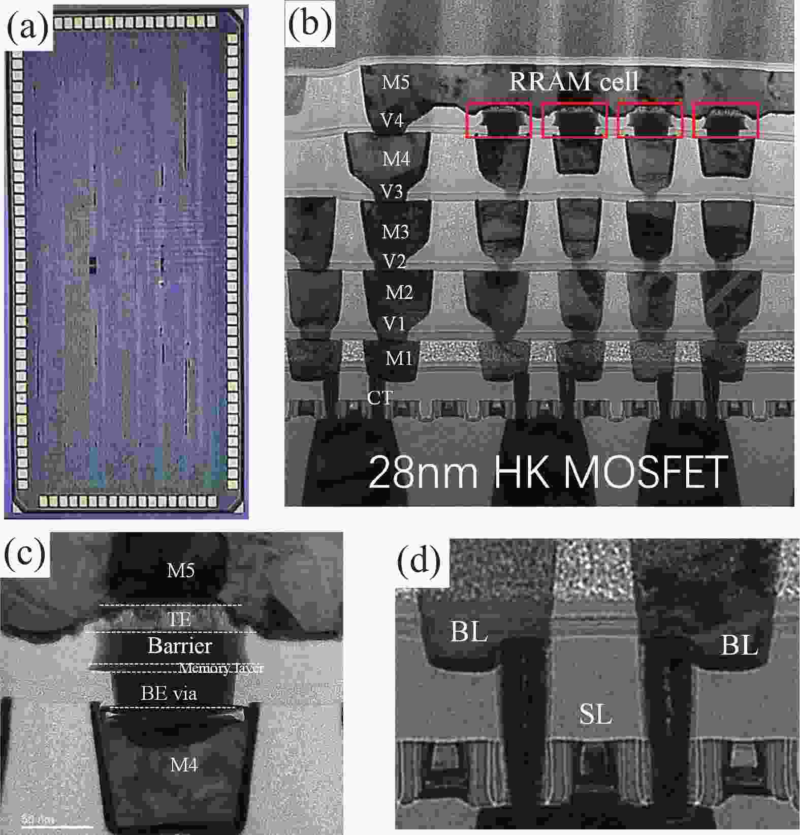
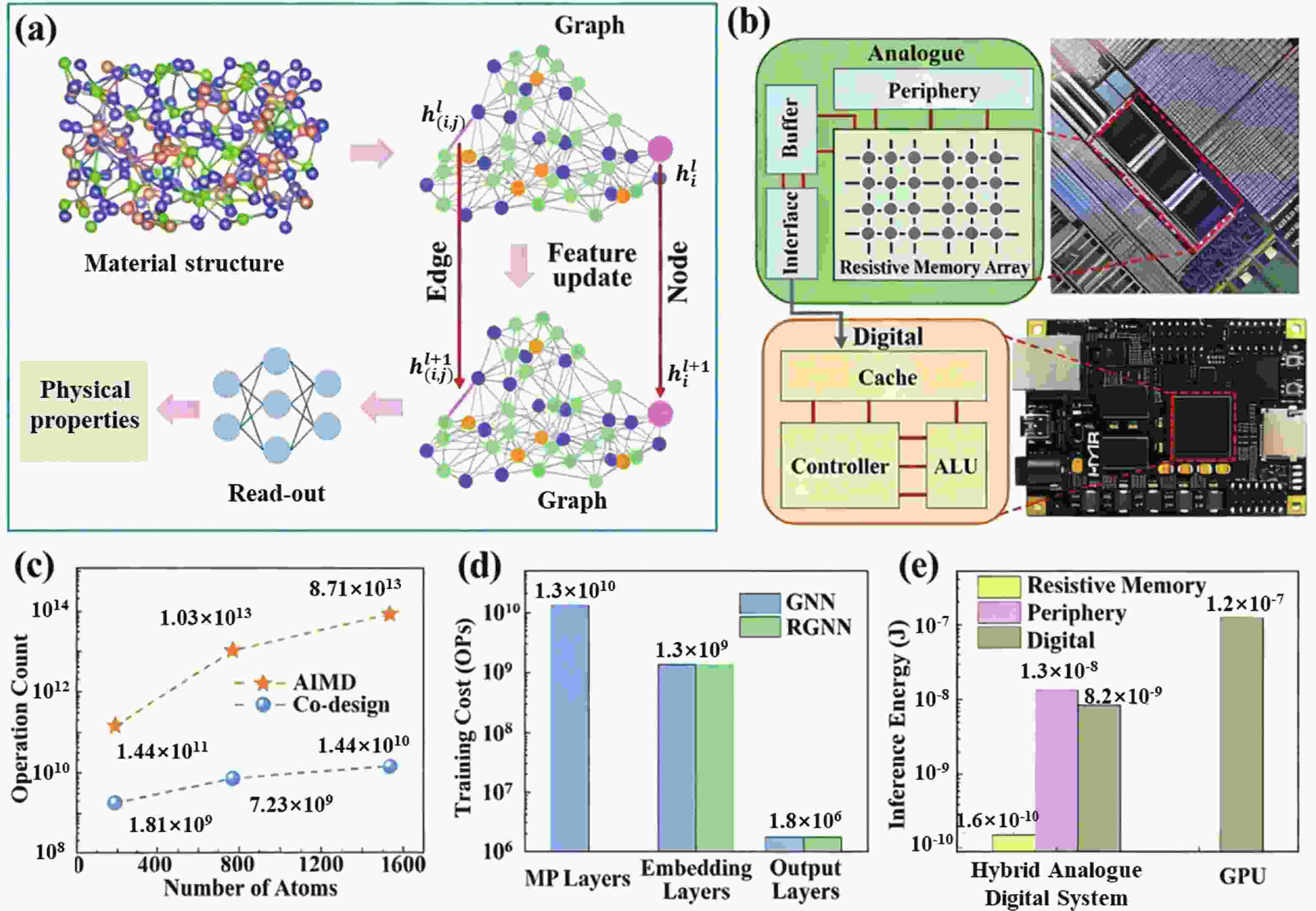
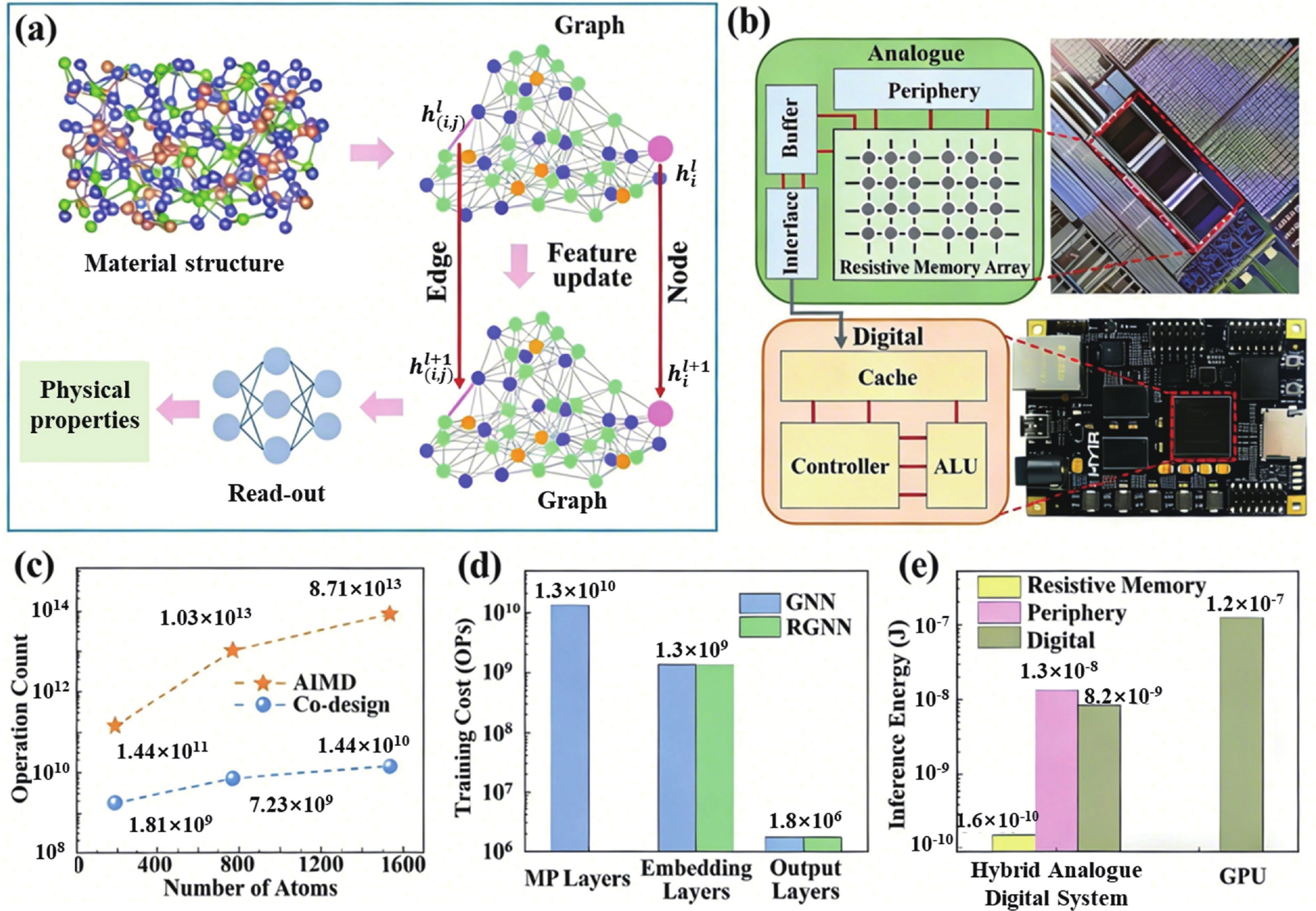
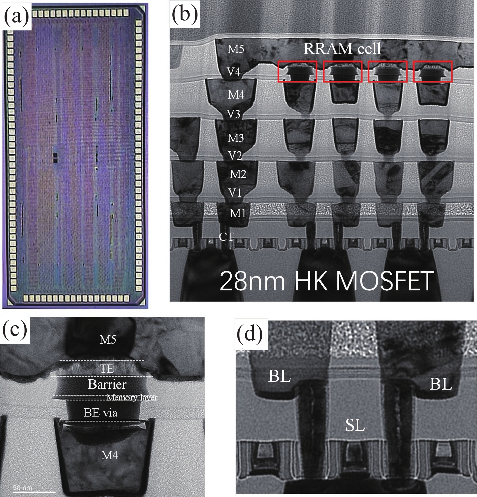
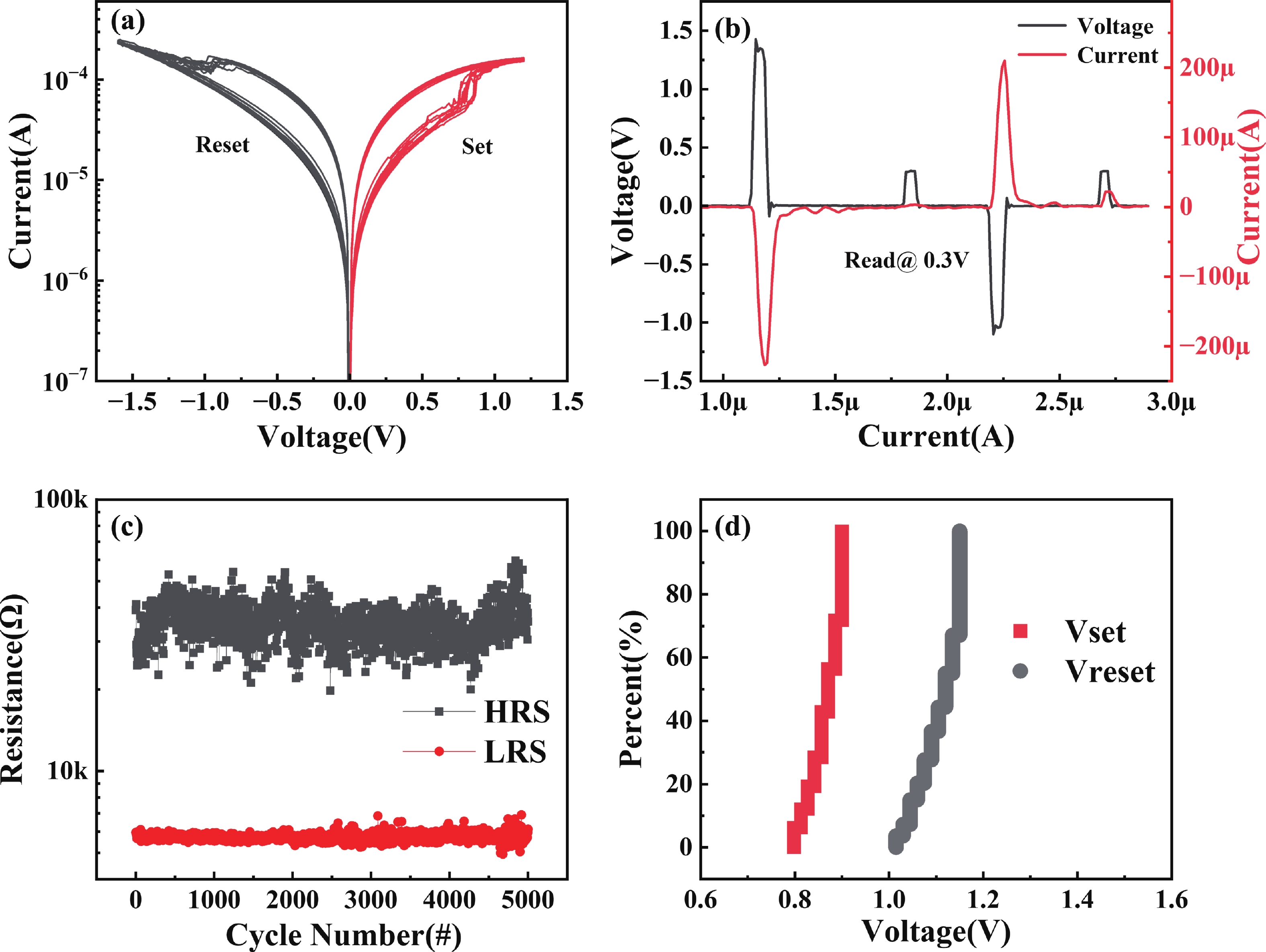
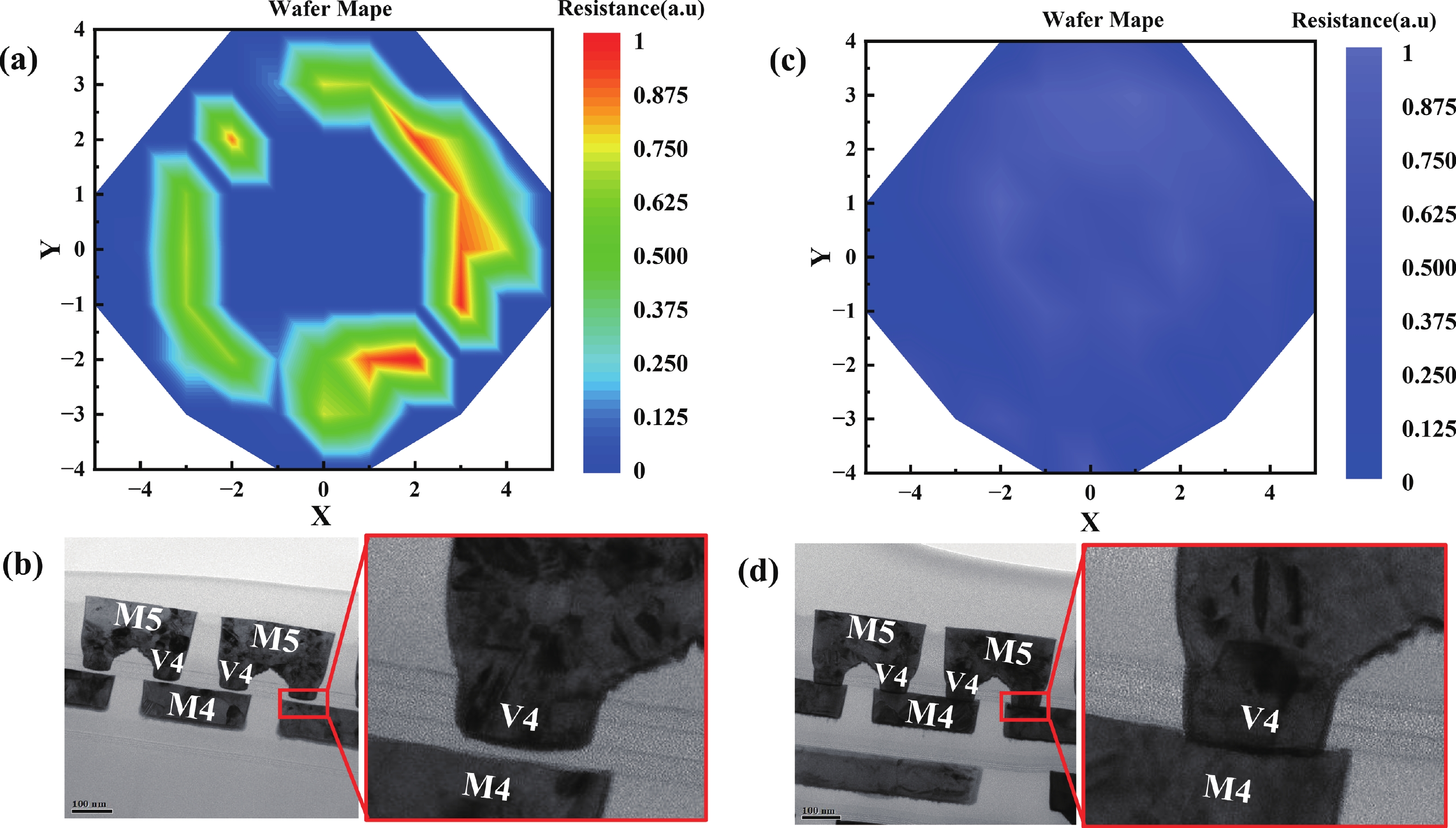
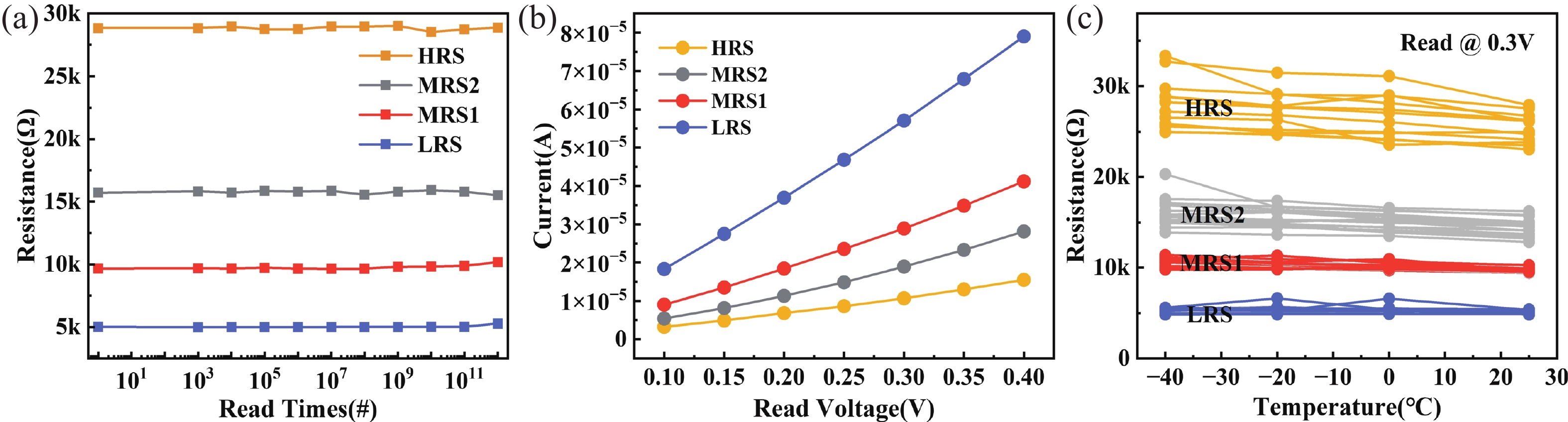
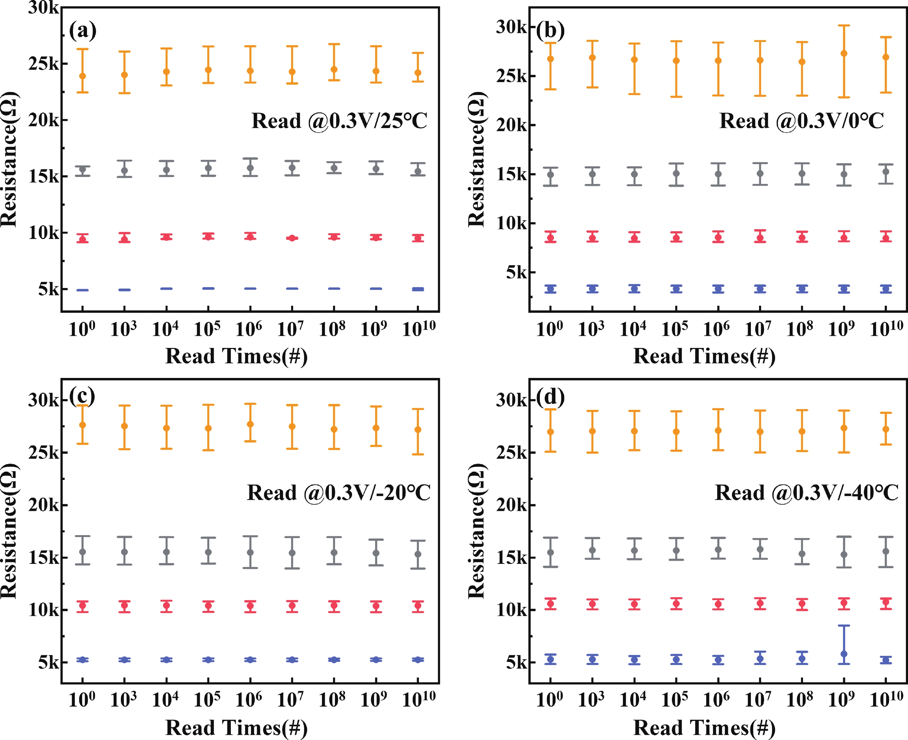
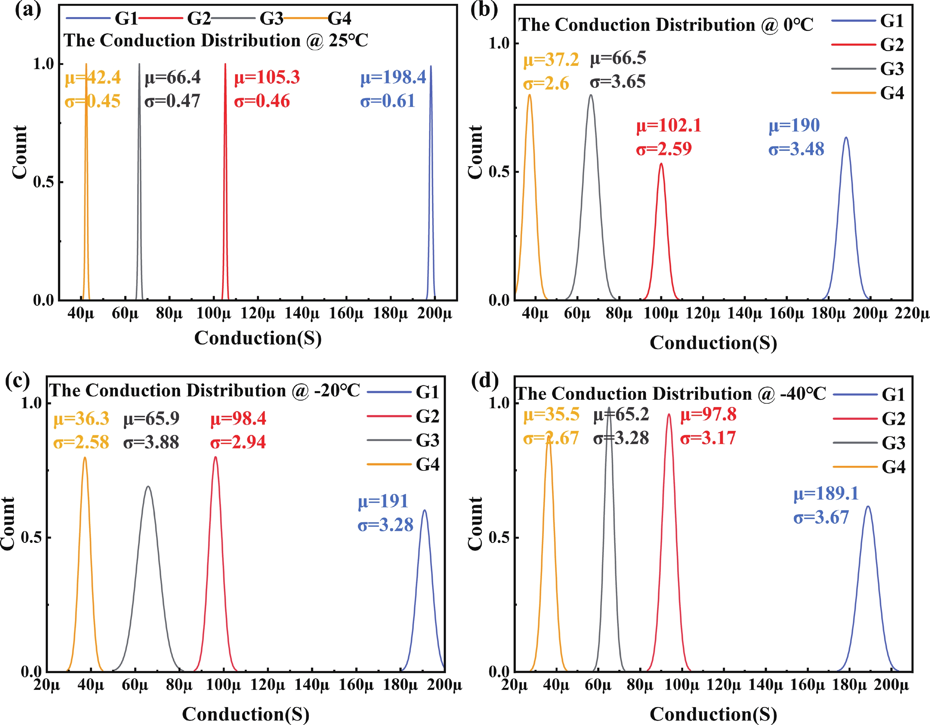
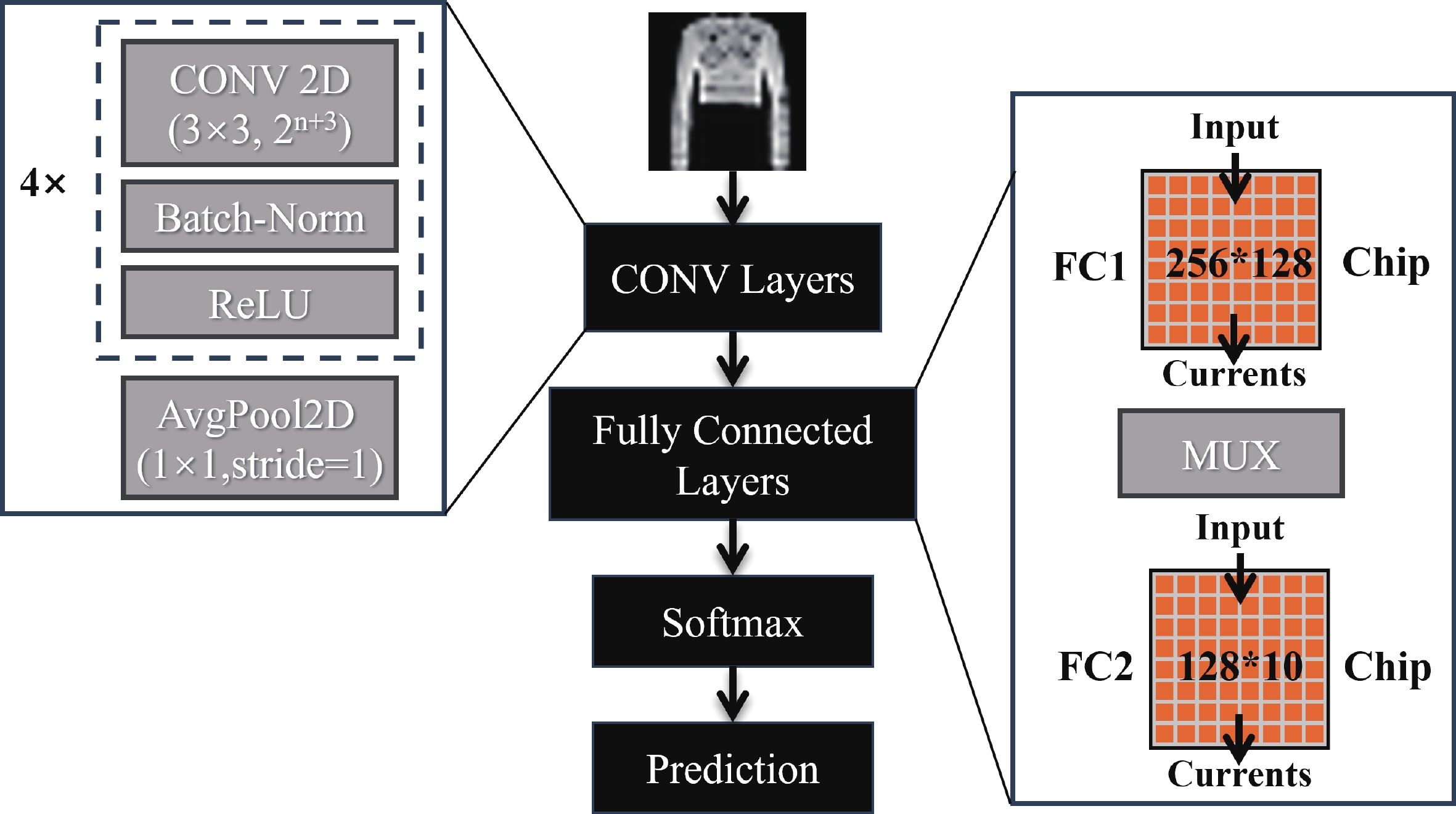
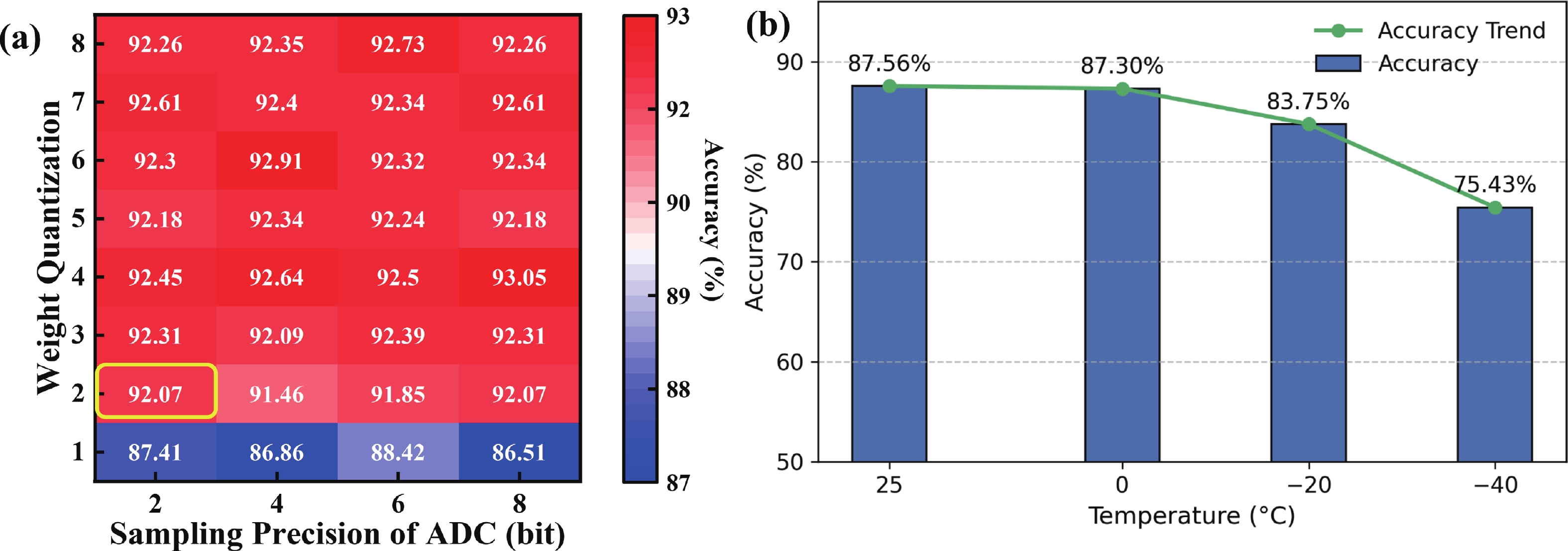
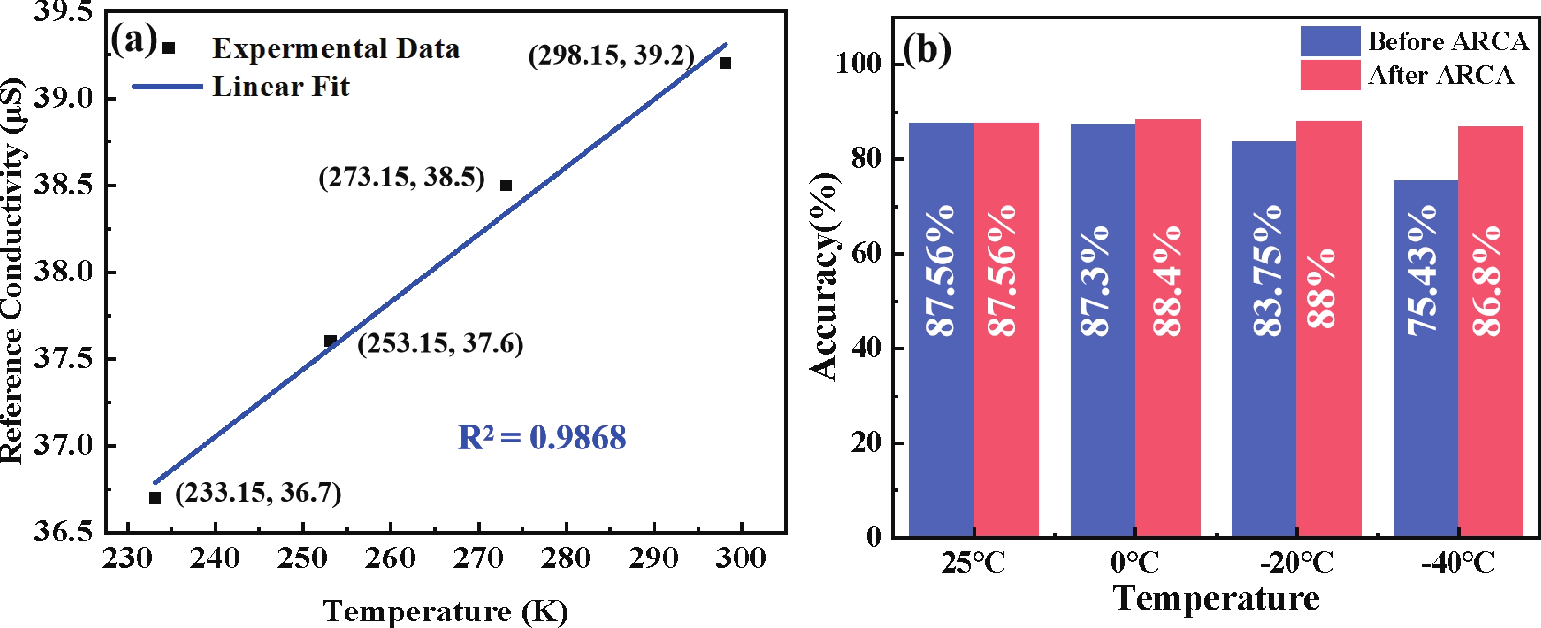
With the widespread application of artificial intelligence (AI) computing in low-temperature scenarios such as deep space and deep sea, RRAM-based edge computing has gradually attracted attention. In this paper, an adaptive reference conductance algorithm (ARCA) is proposed to improve the inference accuracy in low-temperature scenarios due to the conduction drift. The RRAM CIM chips with high read cycles are fabricated based on 28 nm CMOS logic technology, and the read times could reach 1012. By studying the influence of conductance drifting on inference accuracy in low temperature, a model of temperature and optimal reference conductance is proposed. Furthermore, by this model, adaptive selecting optimal reference conductance of analog-to-digital converters (ADCs) to quantize column current of RRAM array under different temperatures. At −40 ℃, the reference accuracy could increase from 75.43% to 86.8%.
J. Semicond.
2026, 47(7): 072401 doi: 10.1088/1674-4926/26030039
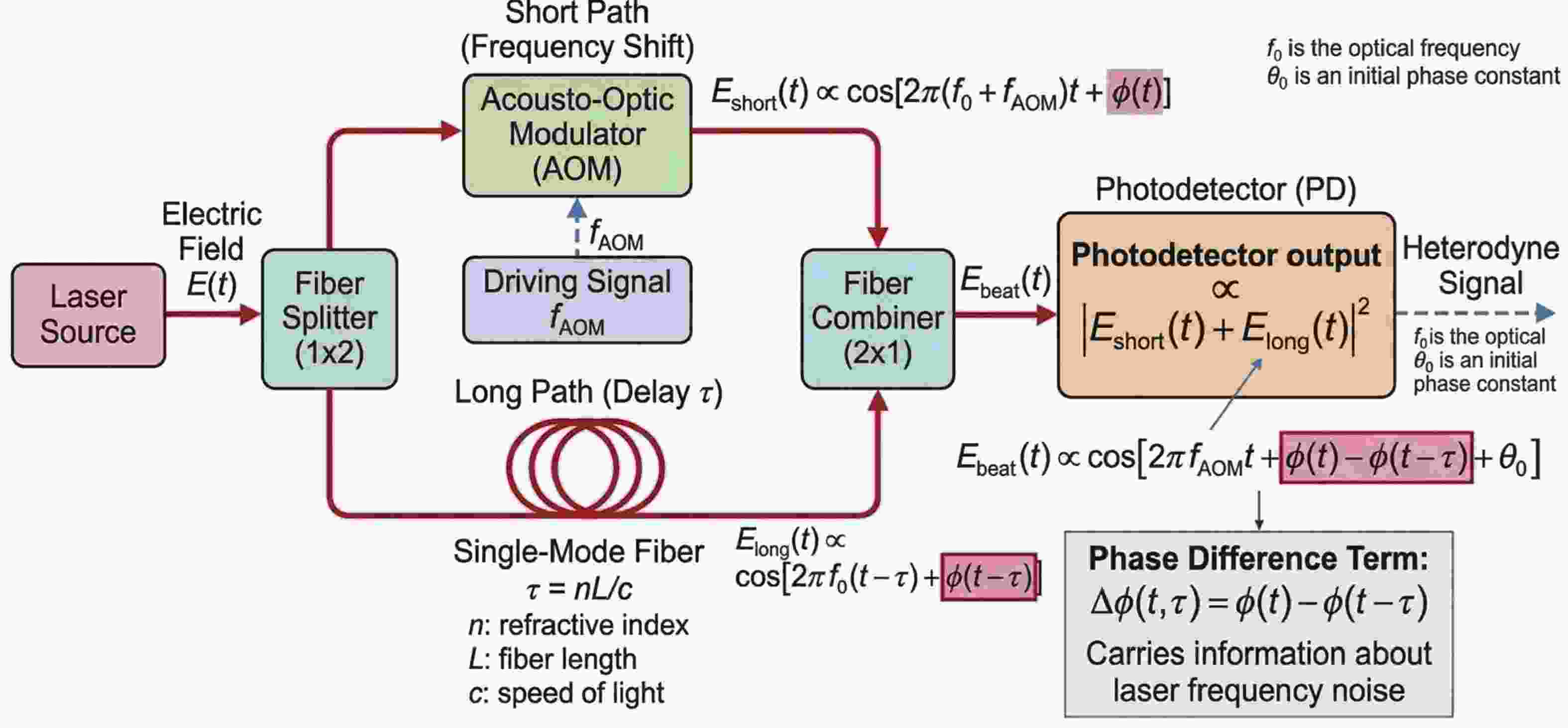
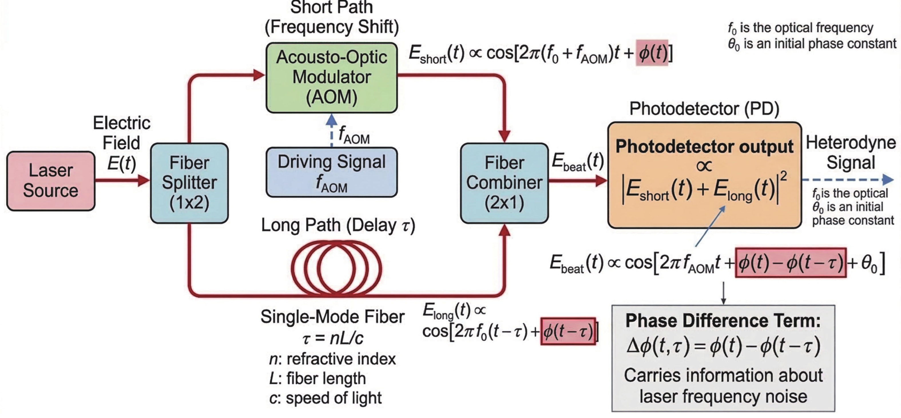
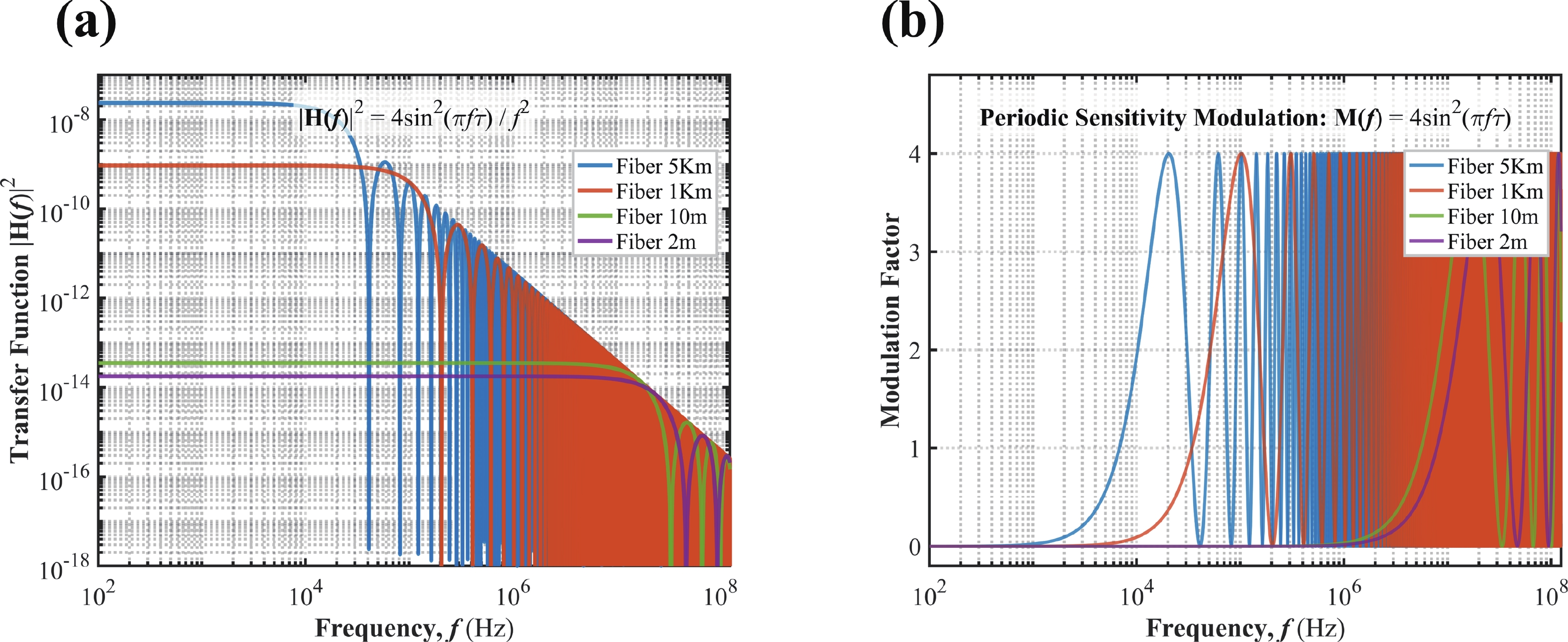
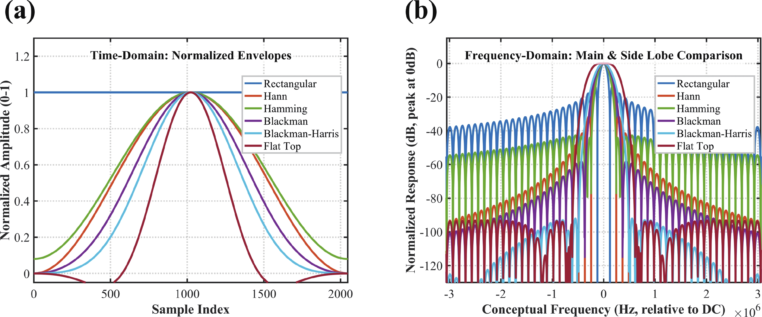
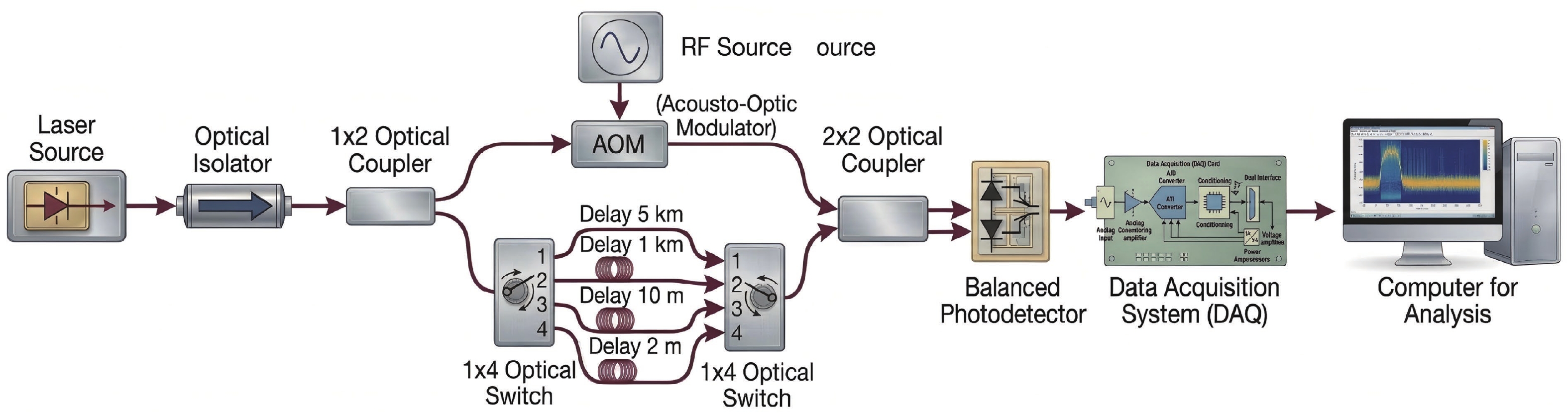
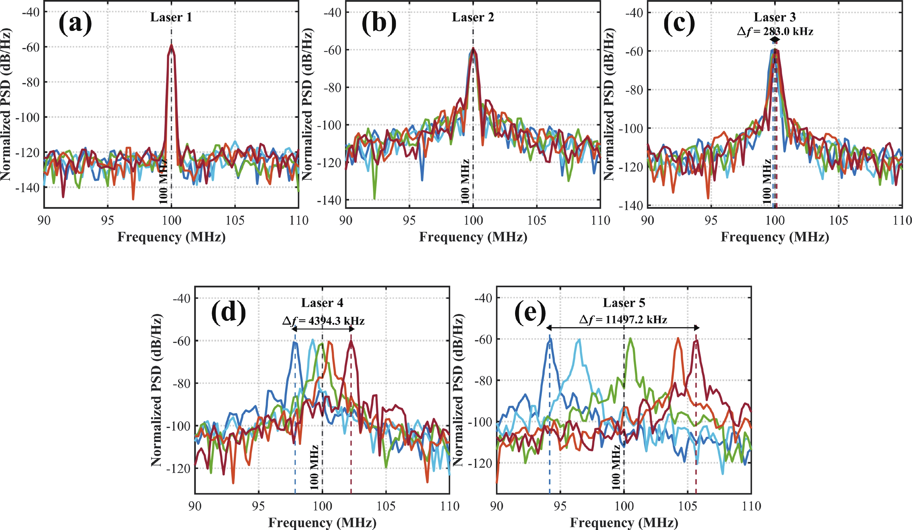
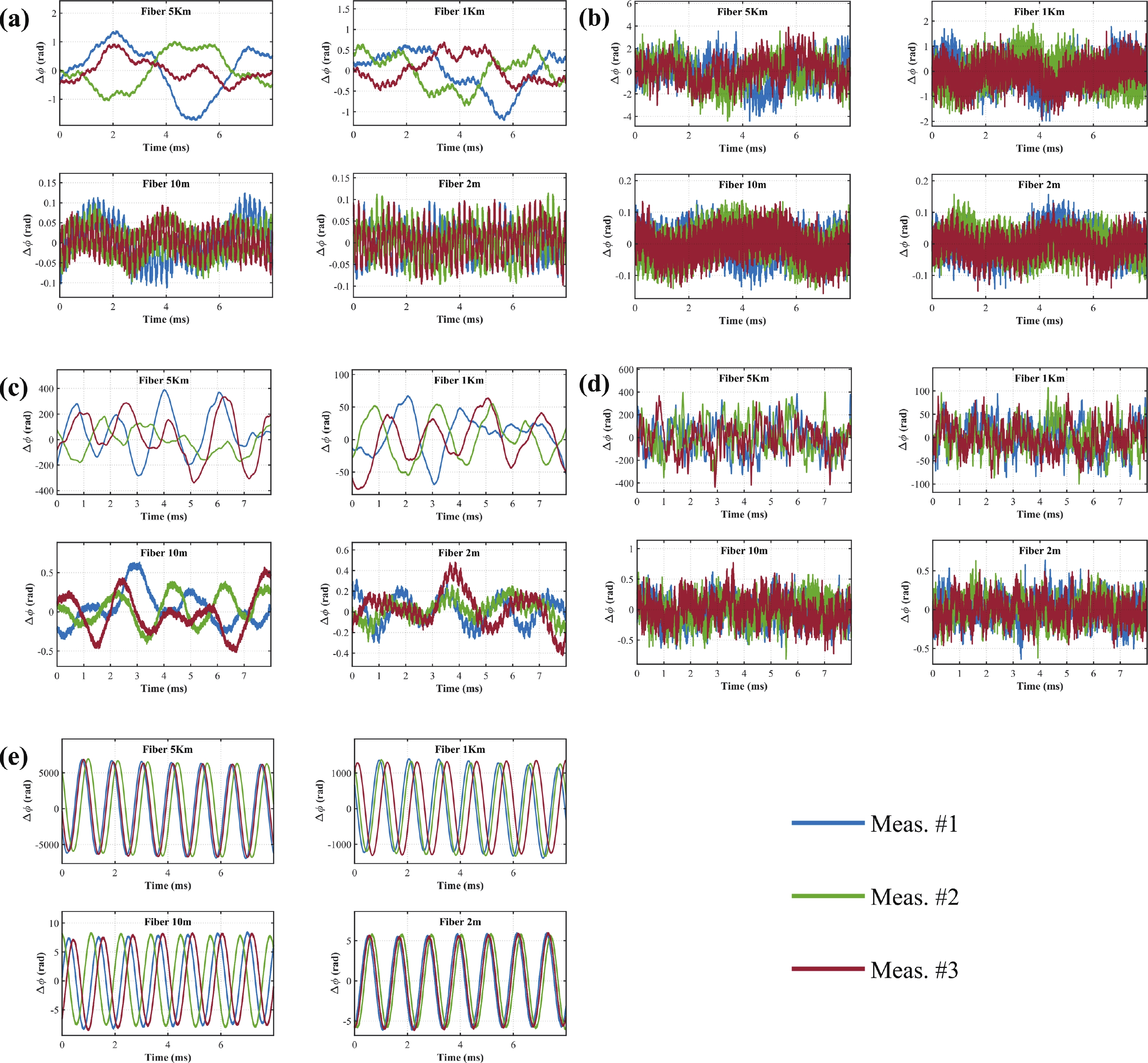
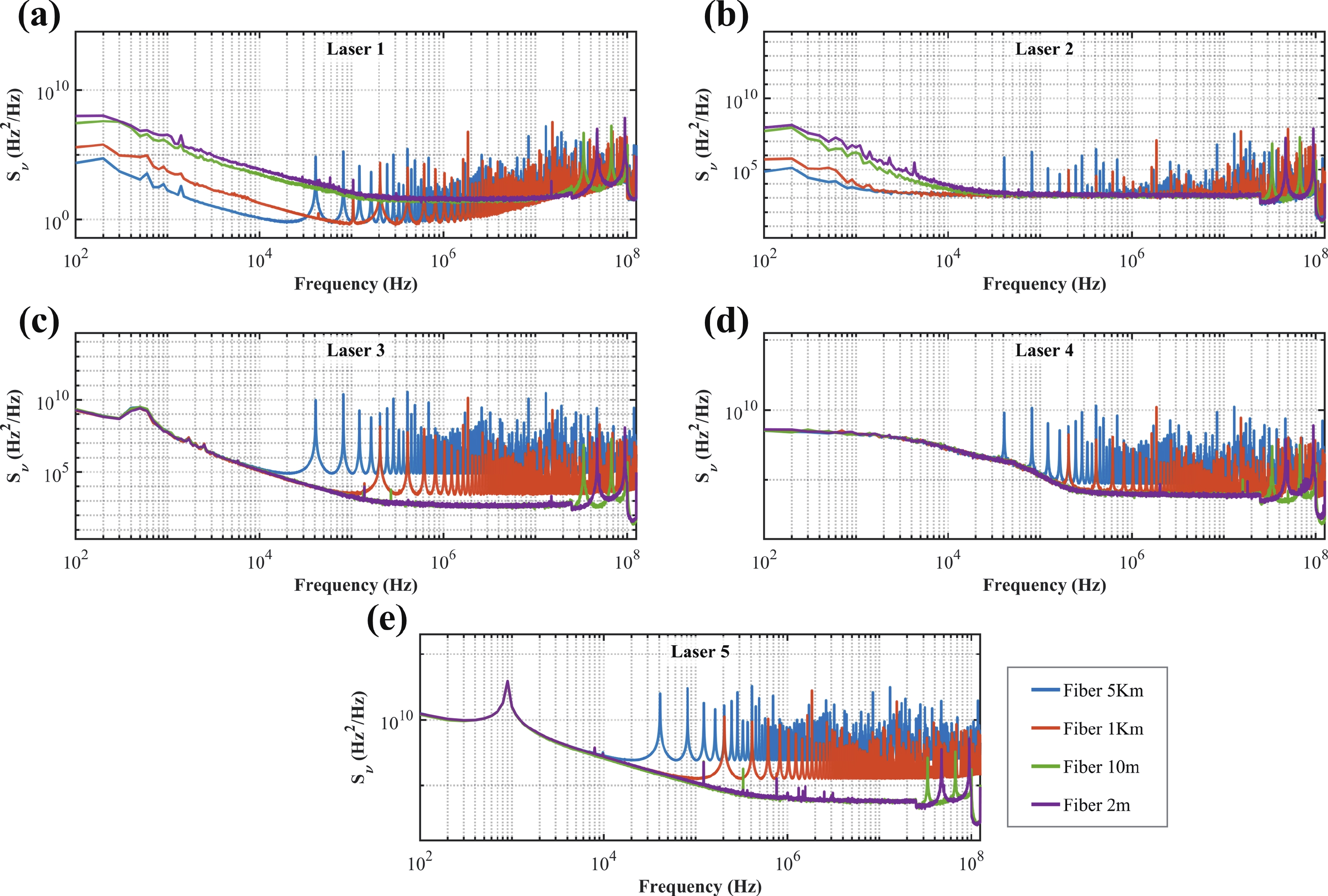
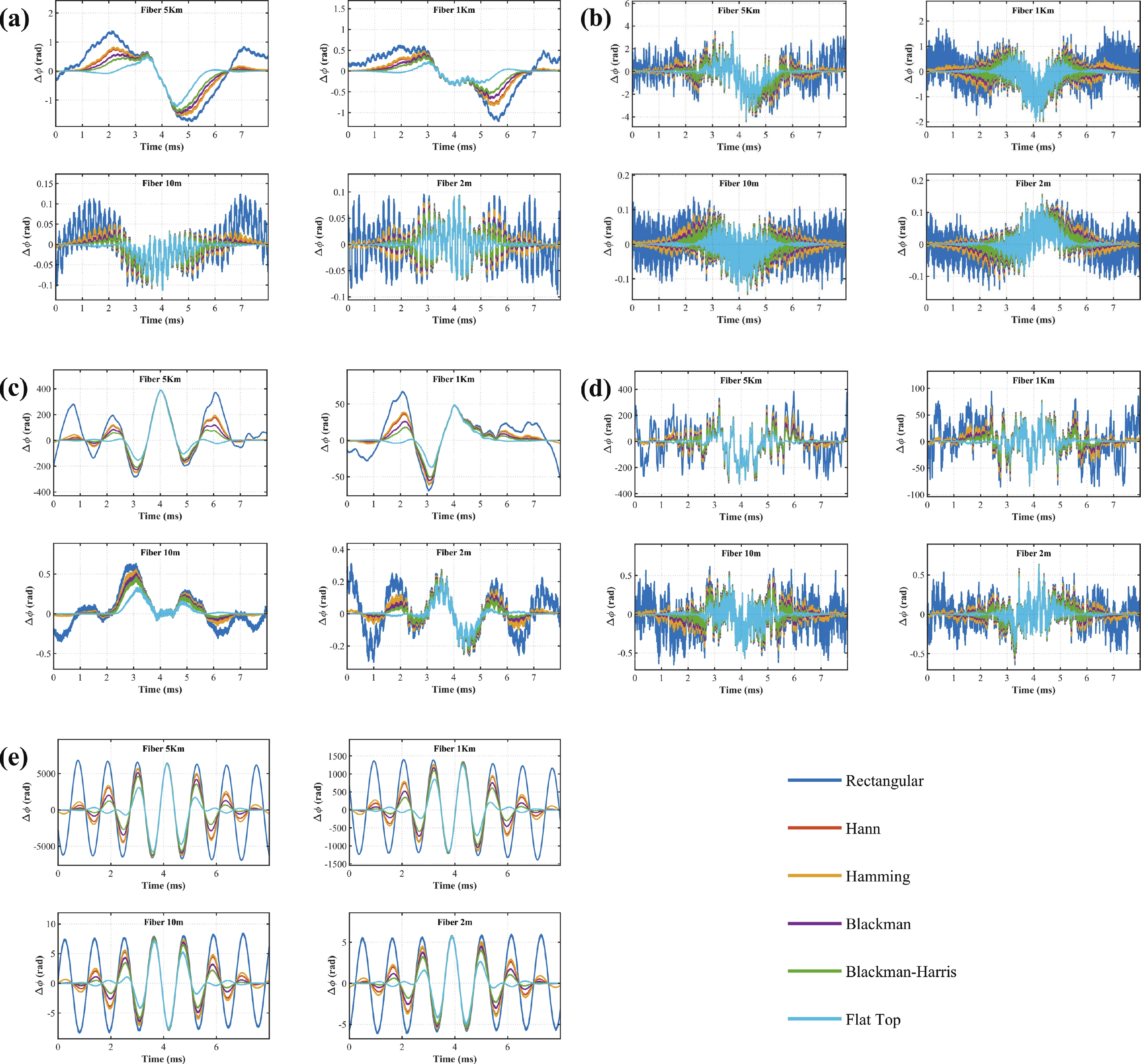
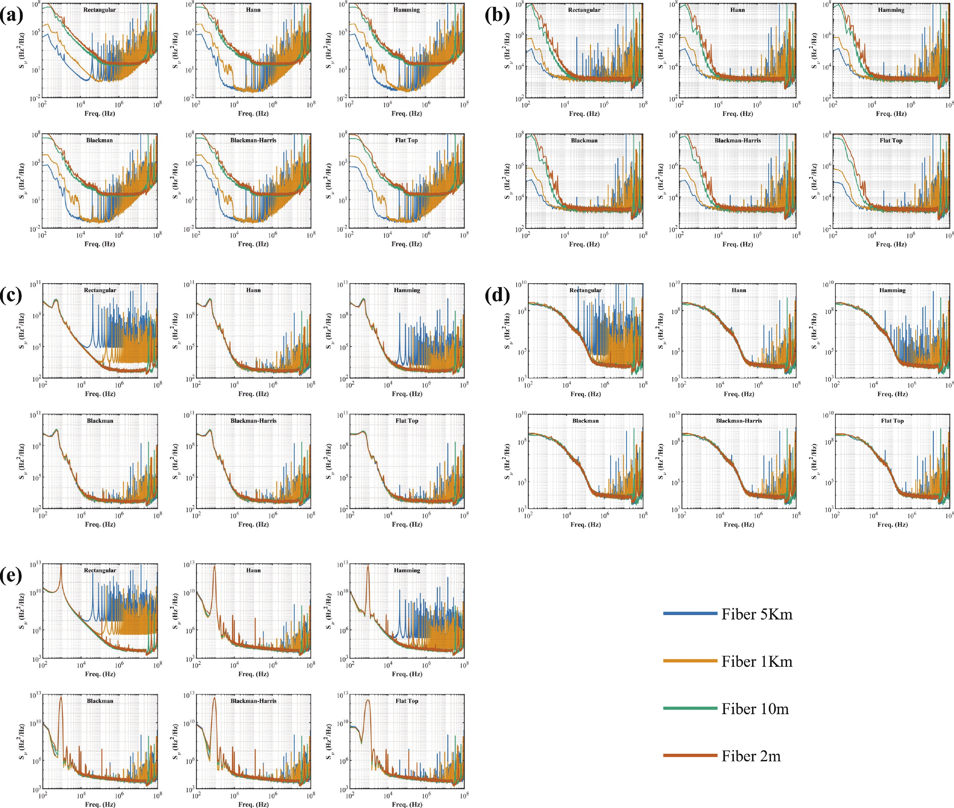
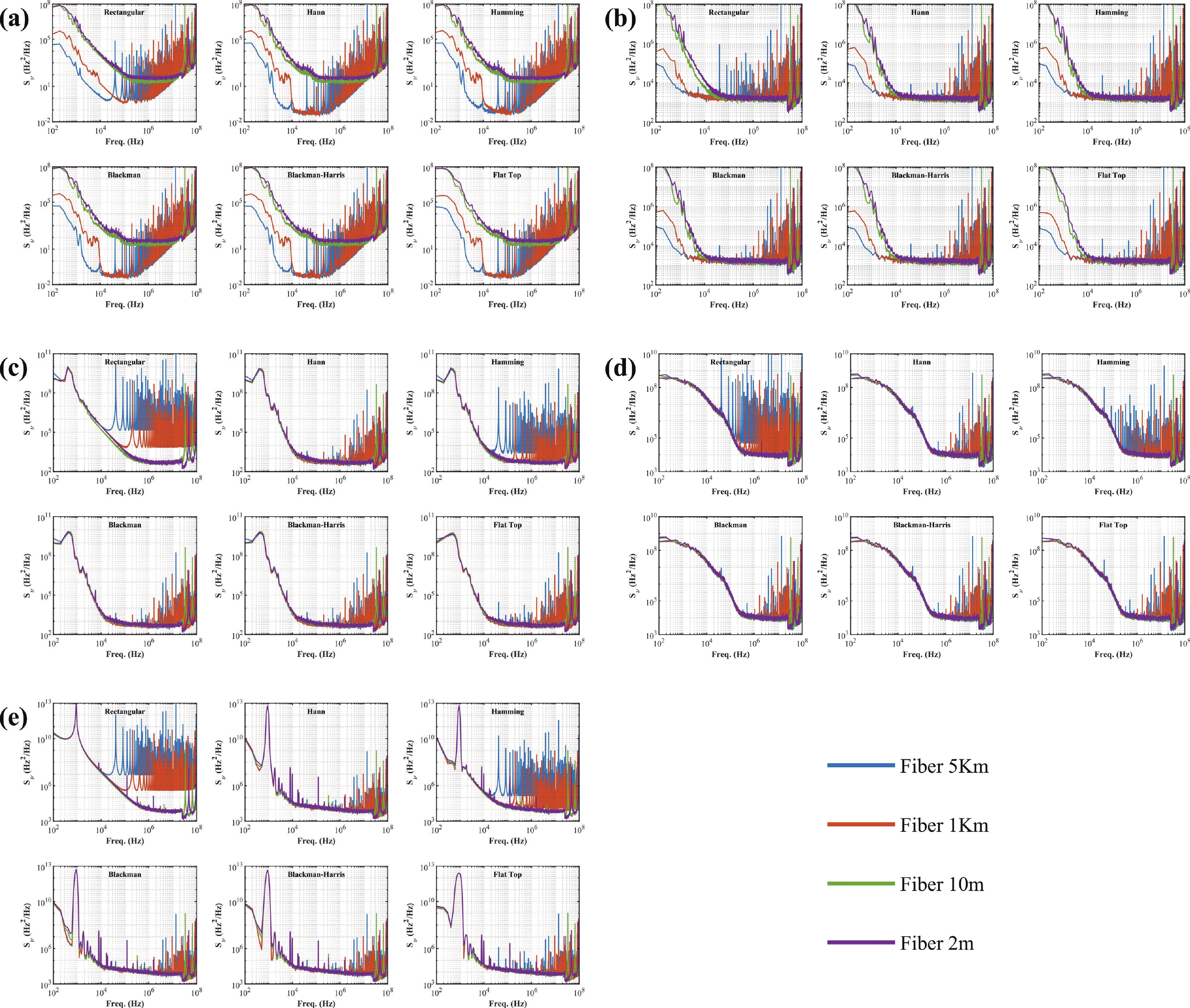
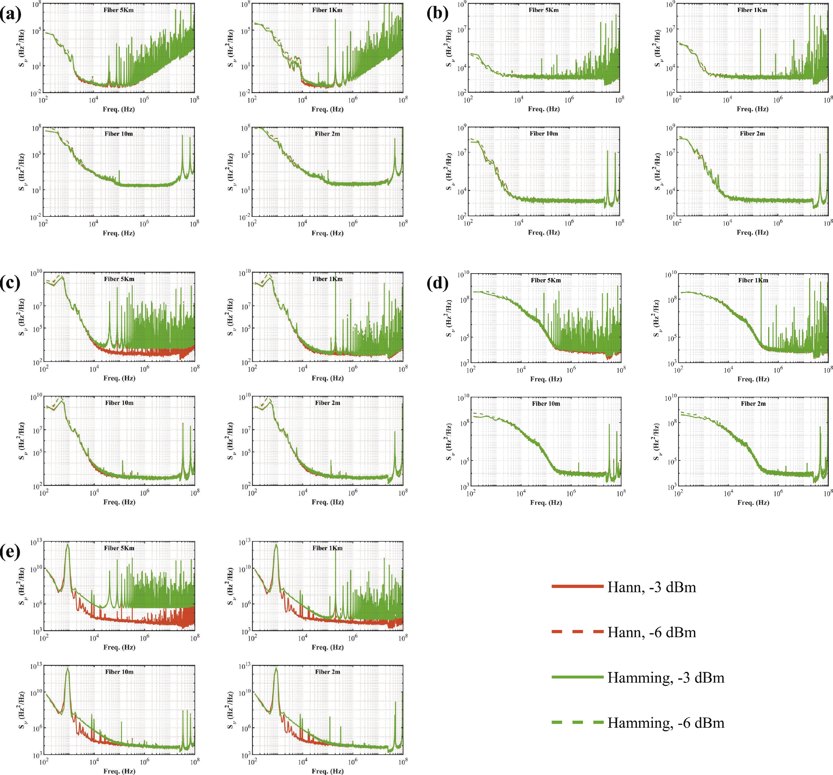
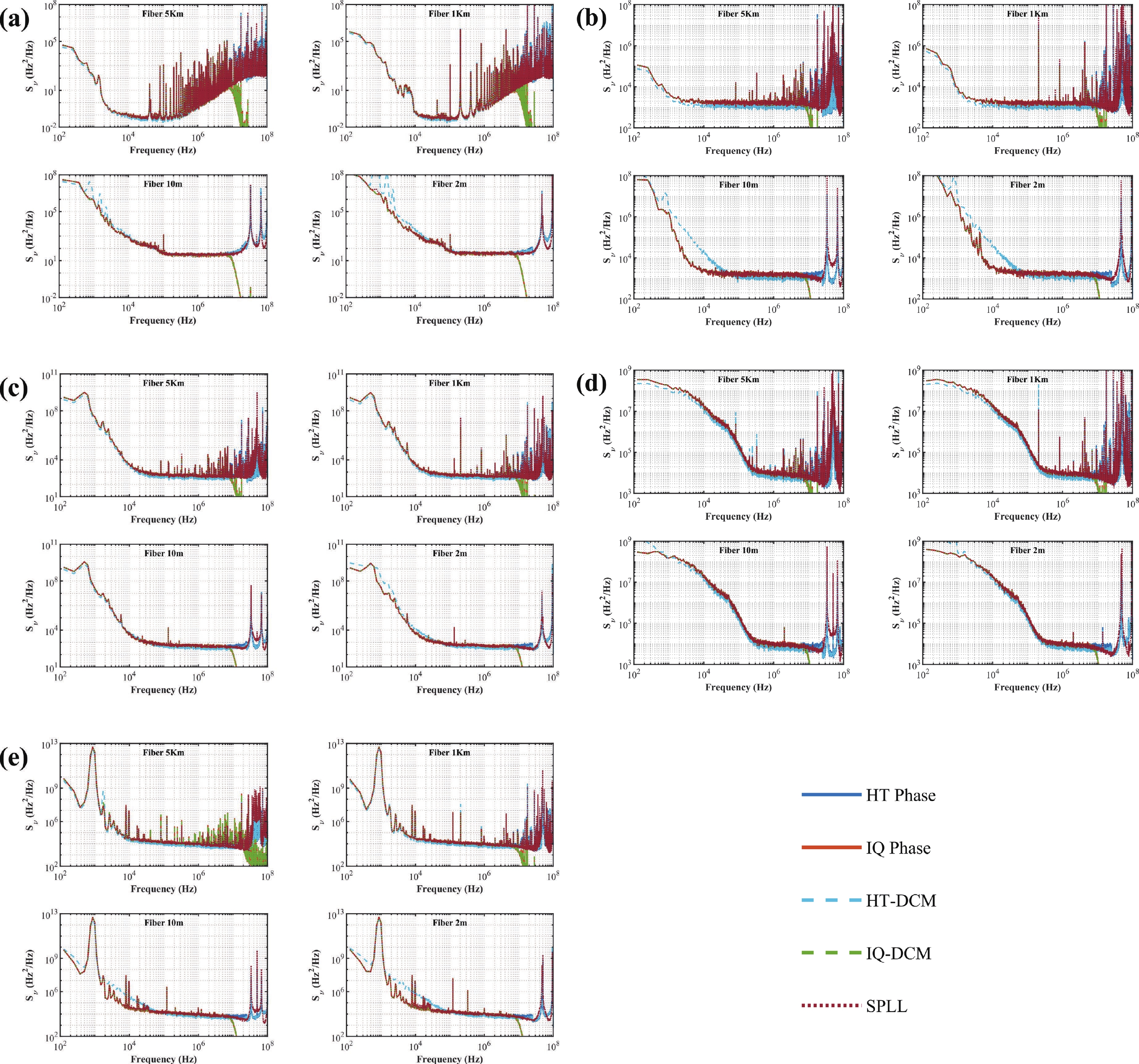
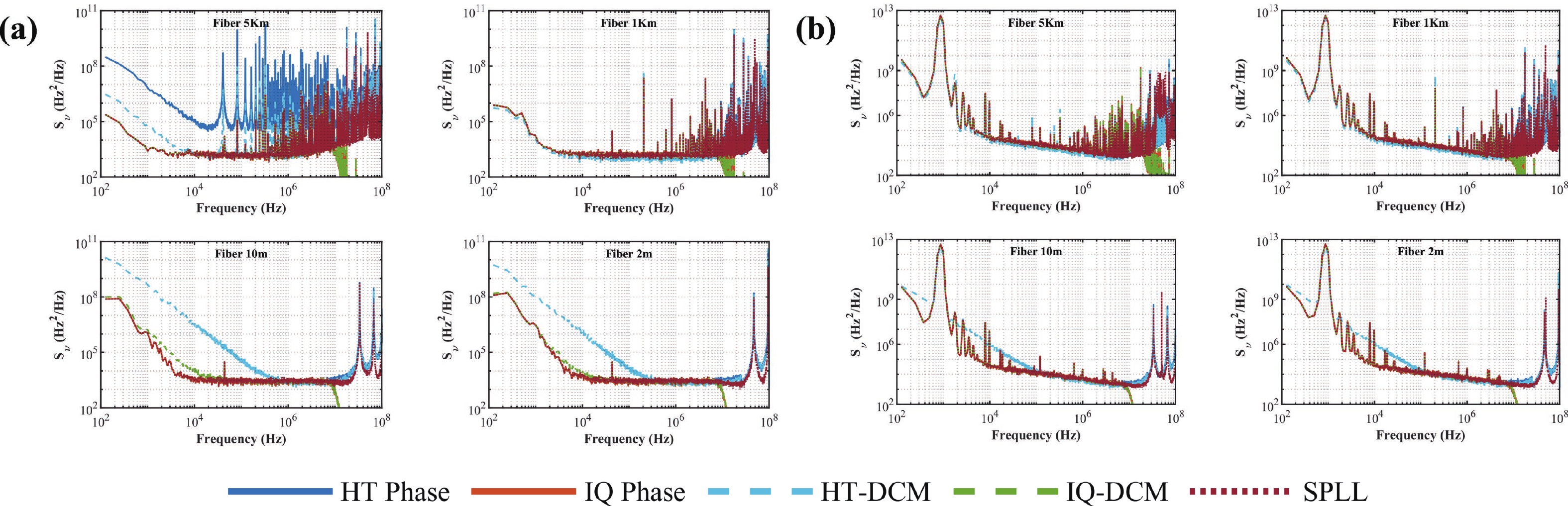
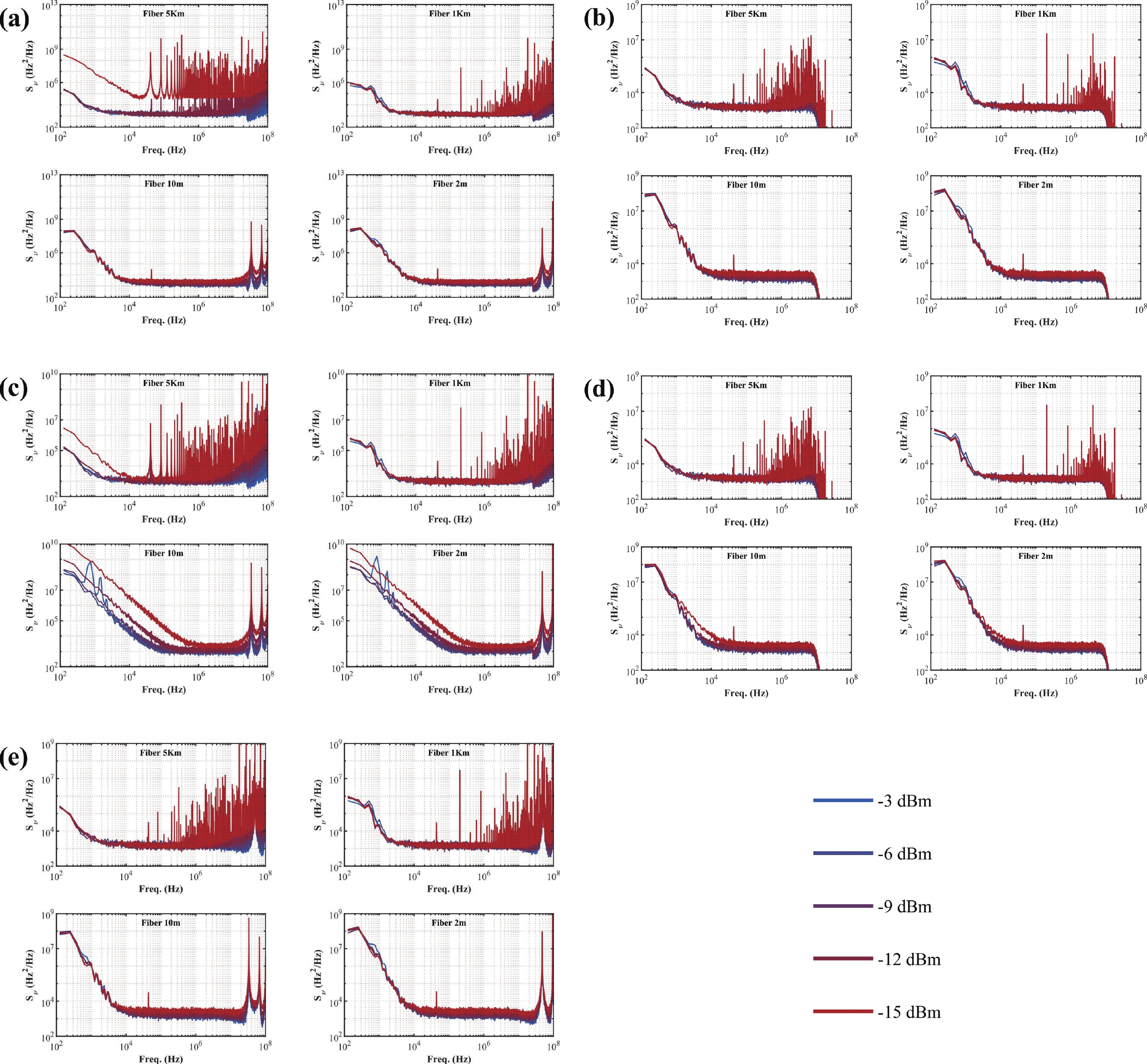
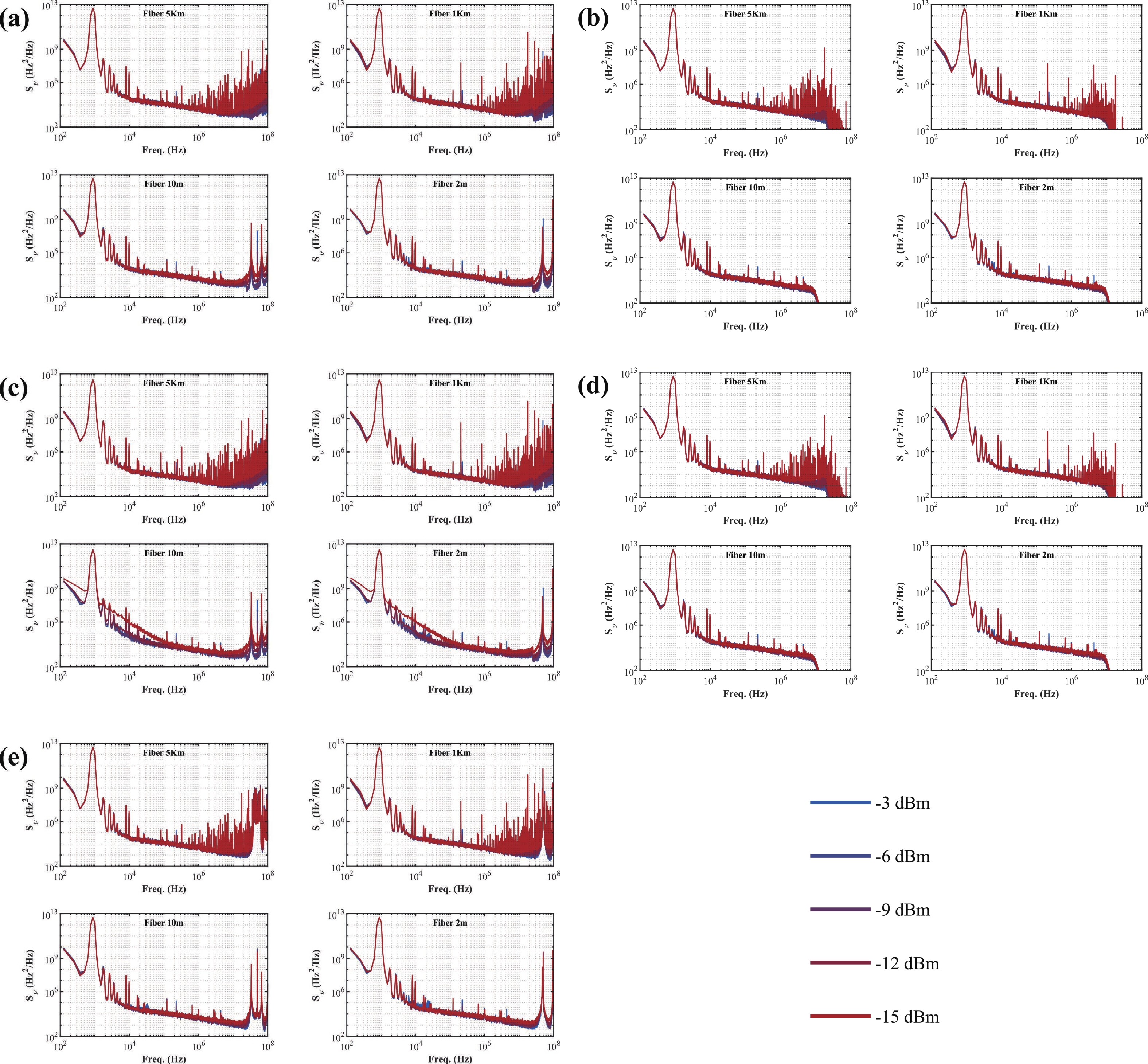
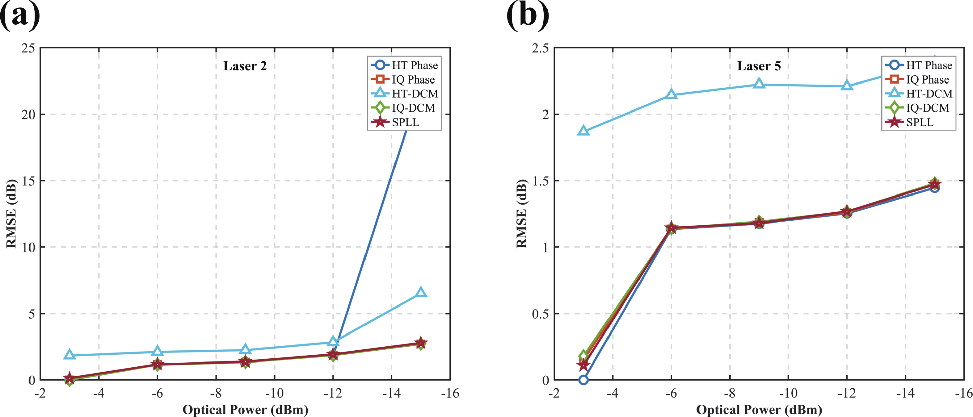
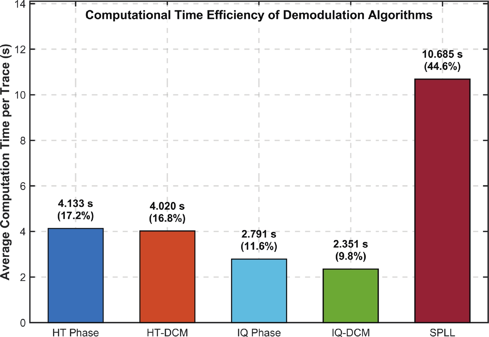
Systematic optimization of the delayed self-heterodyne method for laser frequency noise characterization is investigated across an extensive linewidth range (100 Hz to 10 MHz). By evaluating various fiber lengths, window functions, and five demodulation algorithms, we identify a critical trade-off: long fibers enhance sensitivity for narrow-linewidth lasers but exacerbate spectral leakage in broad-linewidth sources. Our findings demonstrate that Hanning and Blackman windows effectively suppress this leakage, ensuring measurement consistency across different delay lengths. Among the evaluated algorithms, the Hilbert transform offers the superior balance of high-frequency accuracy and computational efficiency. Validated under low-power conditions, this optimized framework provides a robust and power-independent methodology for precise FN analysis, offering significant guidance for high-performance laser development.
J. Semicond.
2026, 47(7): 072402 doi: 10.1088/1674-4926/26030032
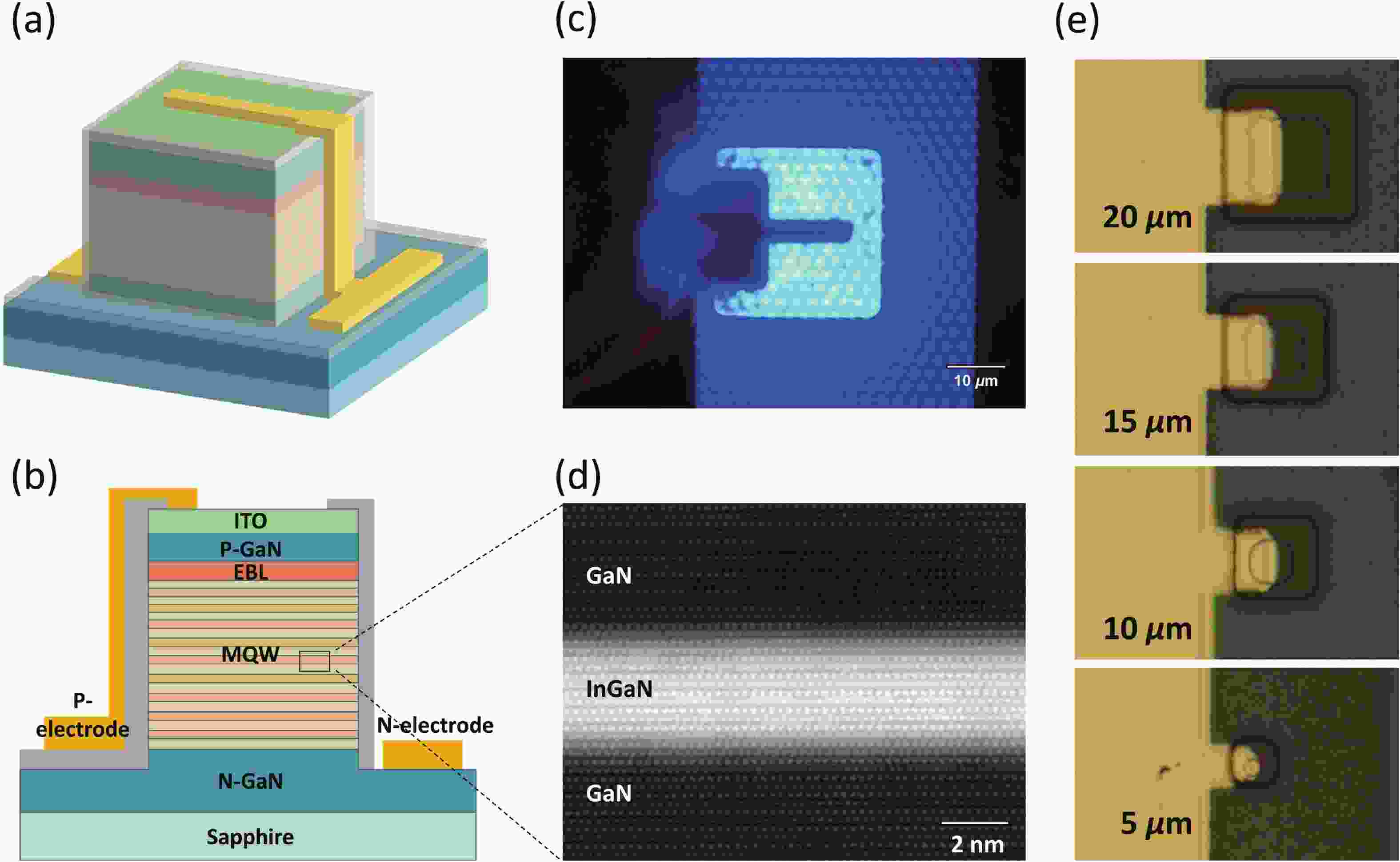
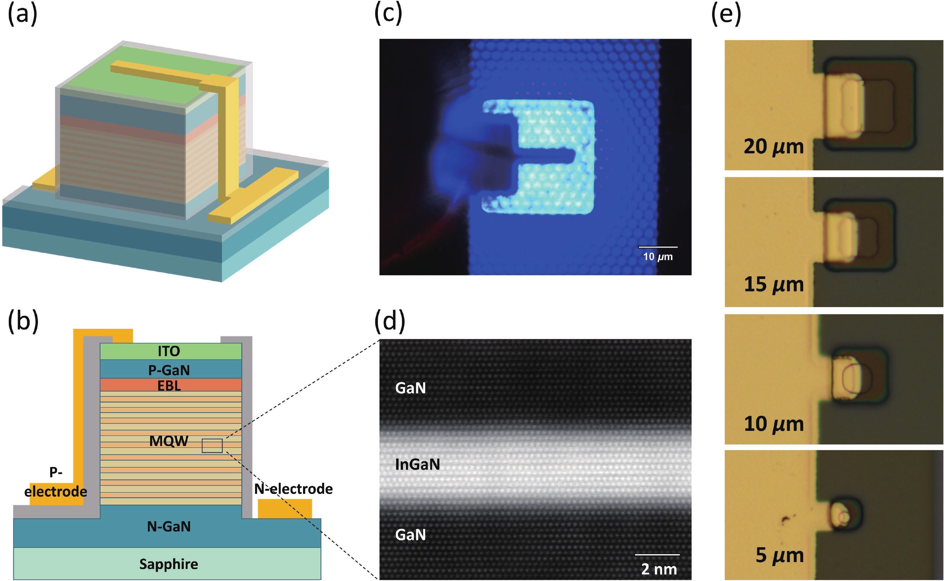
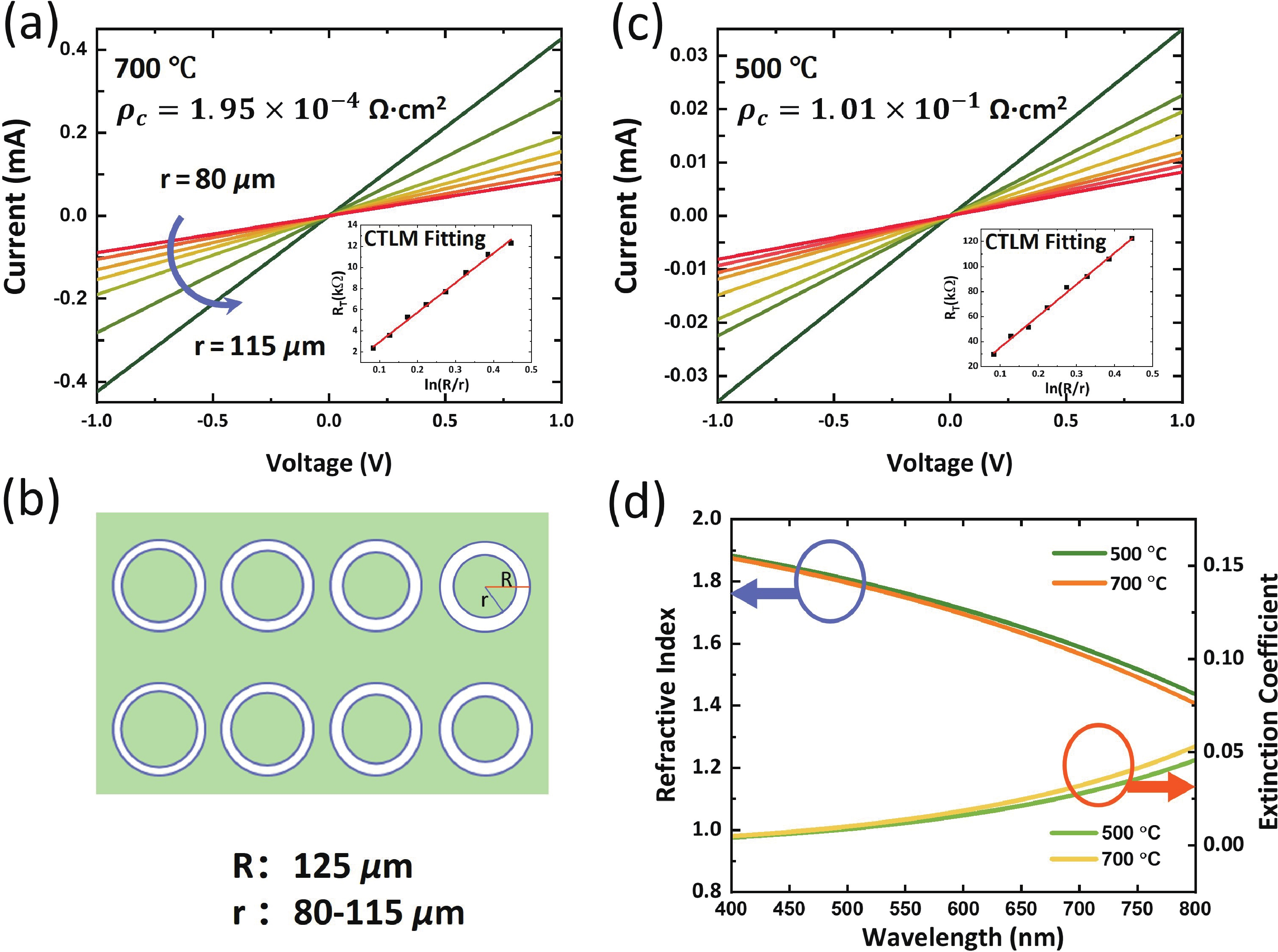
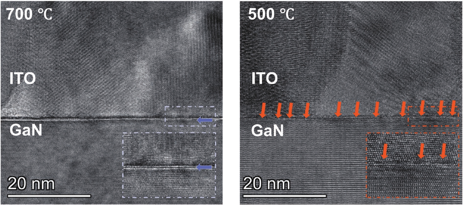
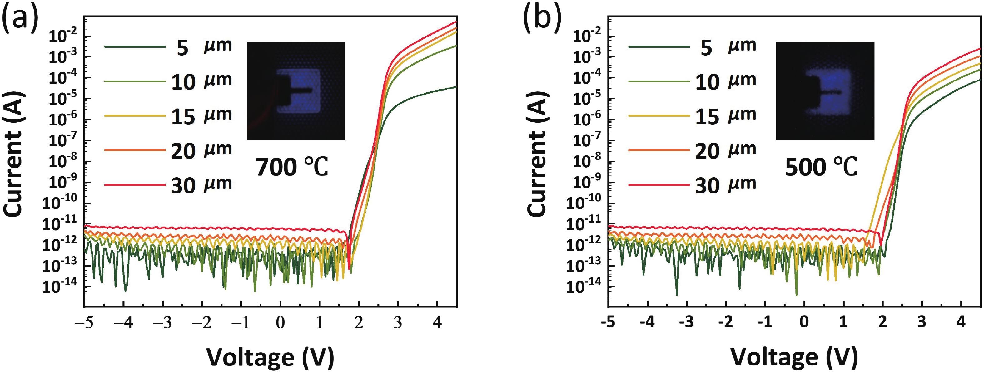
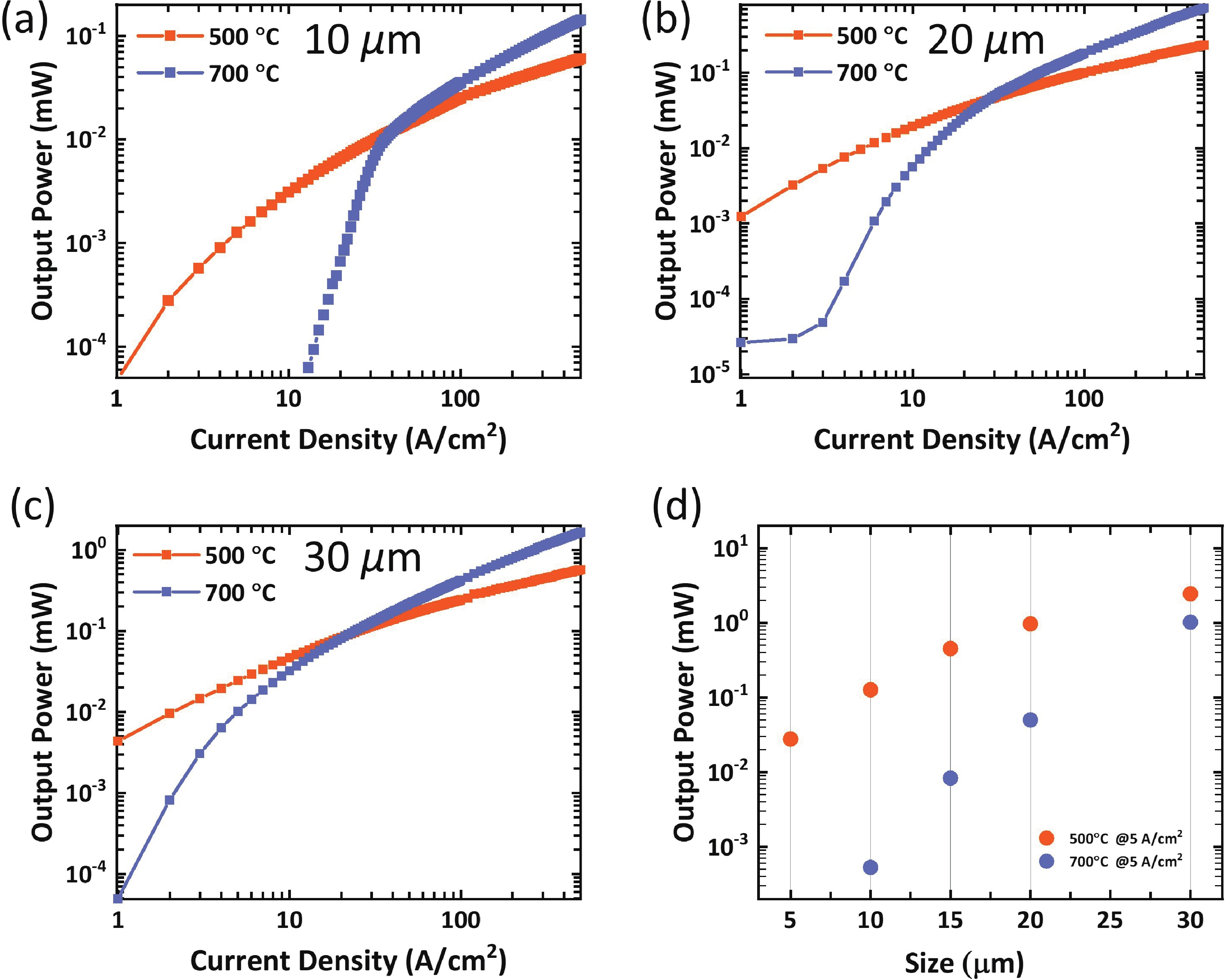
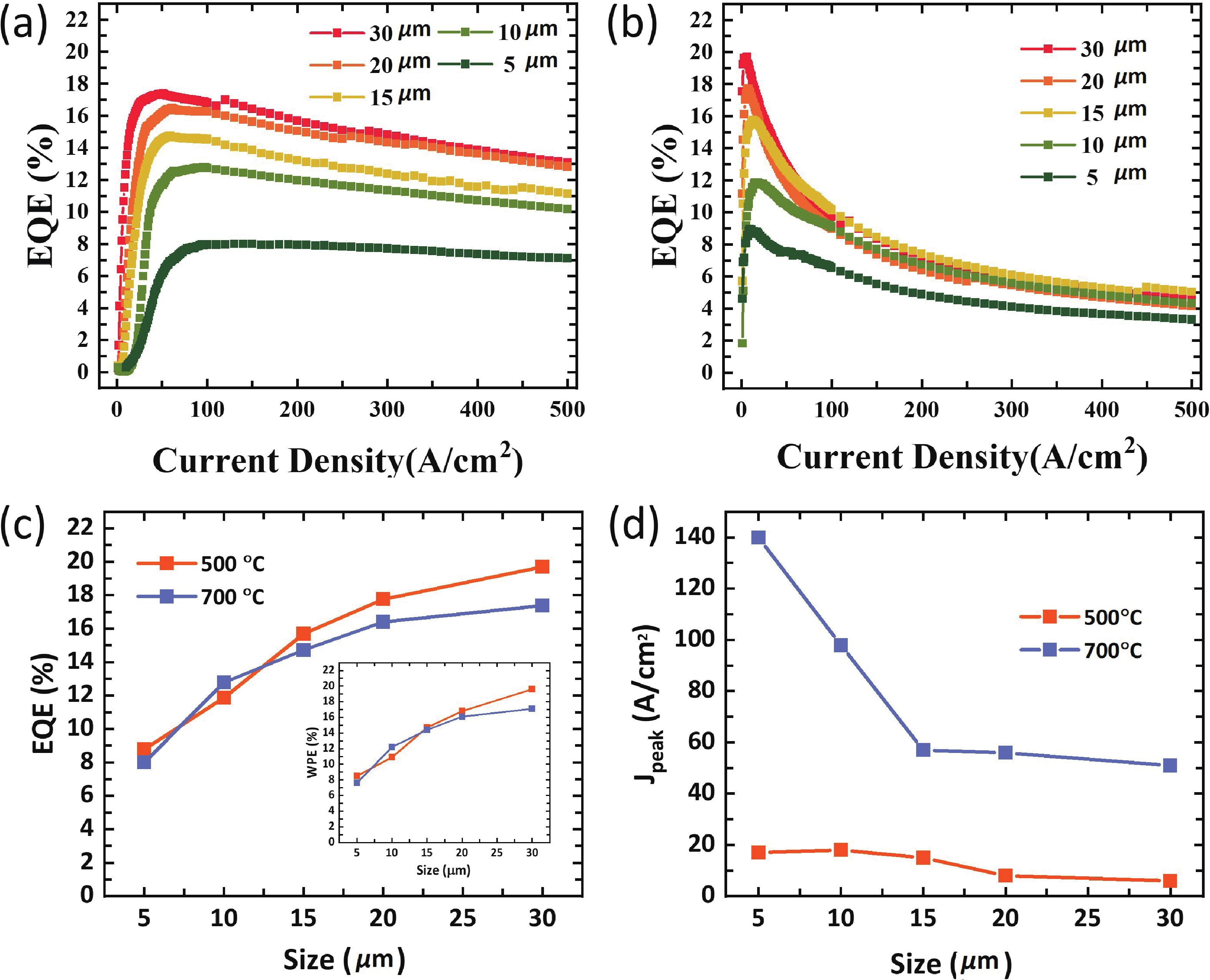
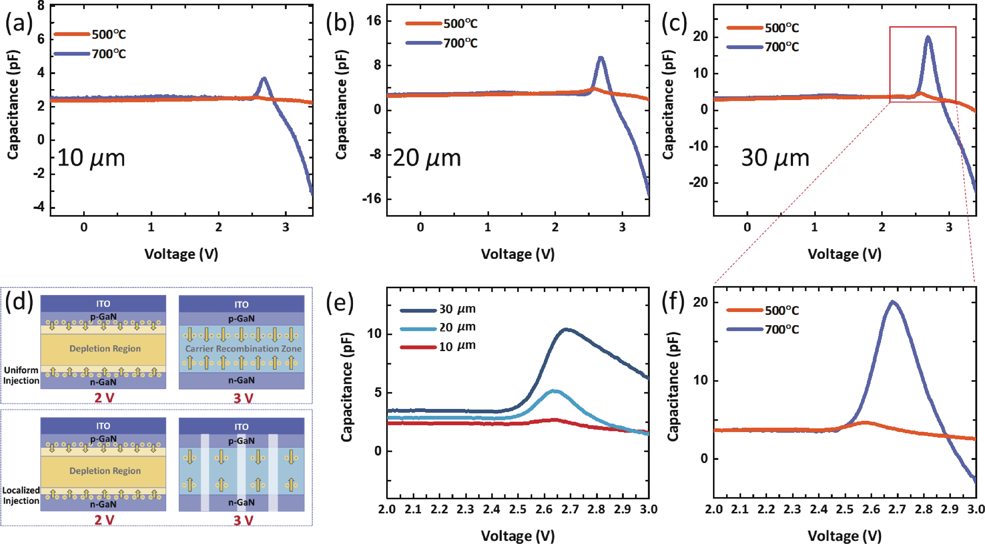
Achieving high emission efficiency at low current densities remains a challenge for micro-LEDs. Here, we demonstrate a controllable interfacial strategy by tuning the annealing temperature of RF-superimposed DC sputtered ITO to modulate carrier injection dynamics. STEM analysis reveals 500 °C annealing triggers discrete substitutional In-atom incorporation into the p-GaN lattice, forming localized nanoscale contact regions. This architecture induces a localized carrier injection mechanism that significantly enhances the efficiency of micro-LEDs at low current densities. Specifically, the 500 °C-annealed 10 μm devices exhibit a dramatic enhancement in light output power (LOP), reaching 1.3 × 10⁻¹ mW at 5 A/cm2, which is significantly higher than the 5.3 × 10⁻⁴ mW measured for 700 °C-annealed devices. Furthermore, the peak efficiency current density (Jpeak) is dramatically shifted from 140 to 17 A/cm2 for 5 μm devices. Capacitance−voltage analysis further corroborates the localized carrier injection mechanism. These findings establish contact interfacial modulation as a robust strategy for optimizing micro-LEDs in low-power display applications and tailoring device-level performance across broader optoelectronics.
J. Semicond.
2026, 47(7): 072501 doi: 10.1088/1674-4926/26010034
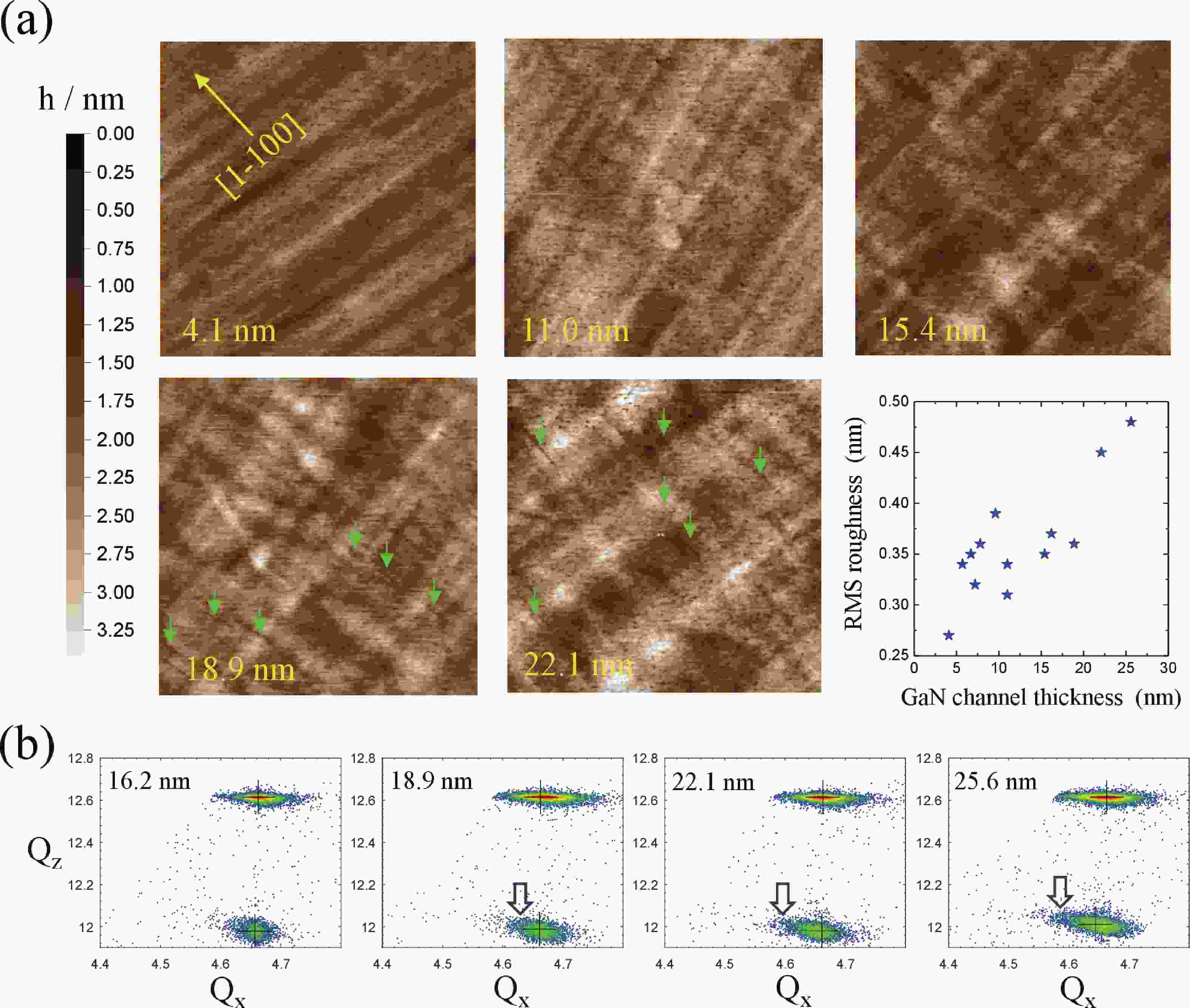
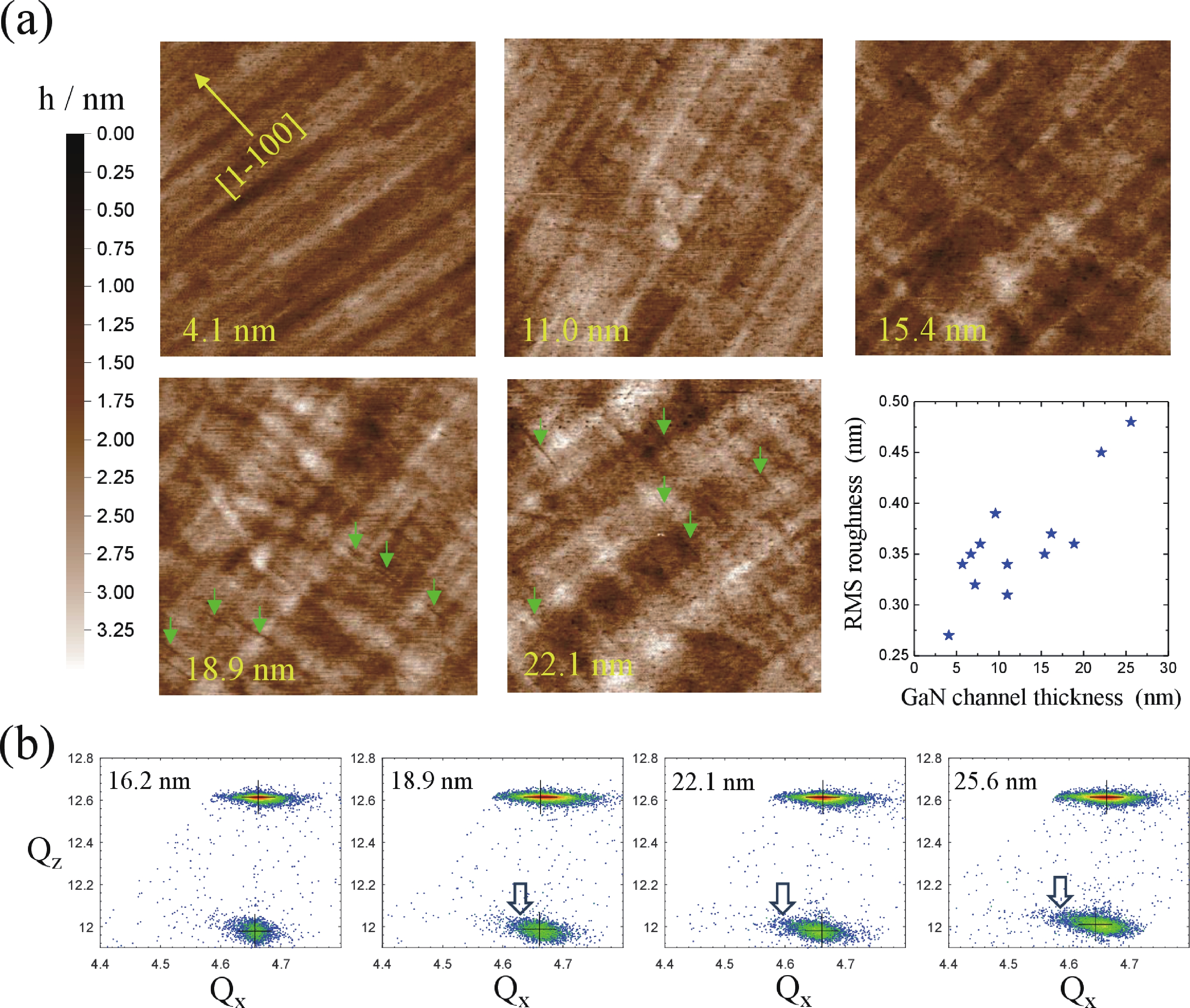
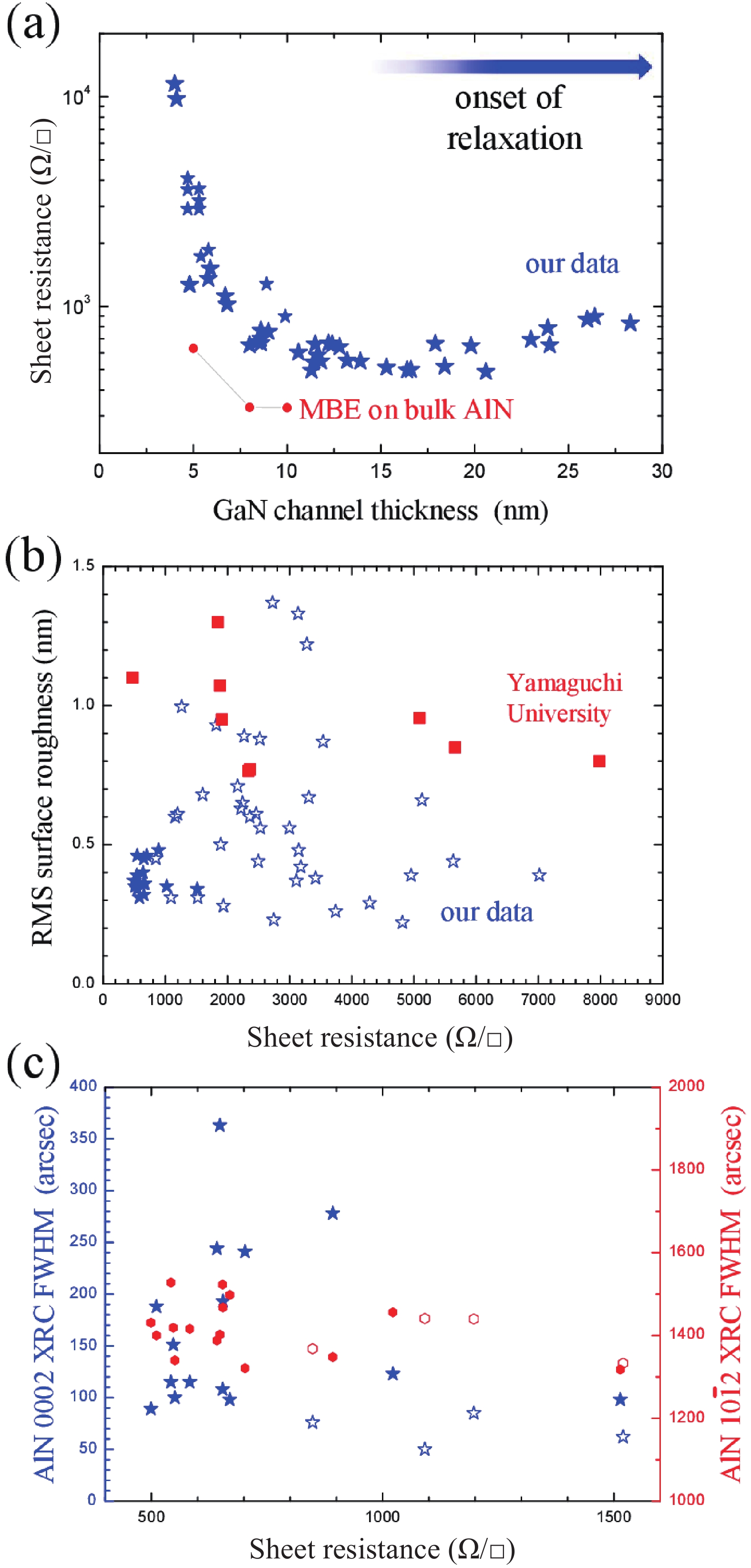
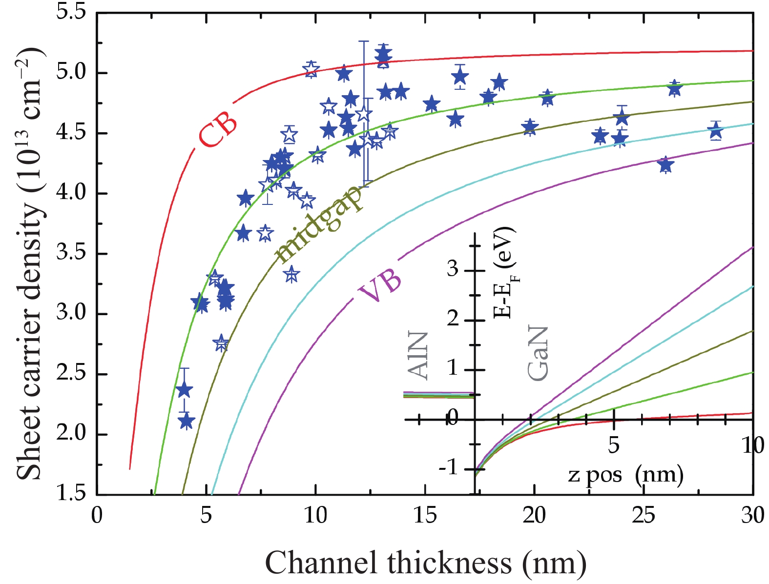
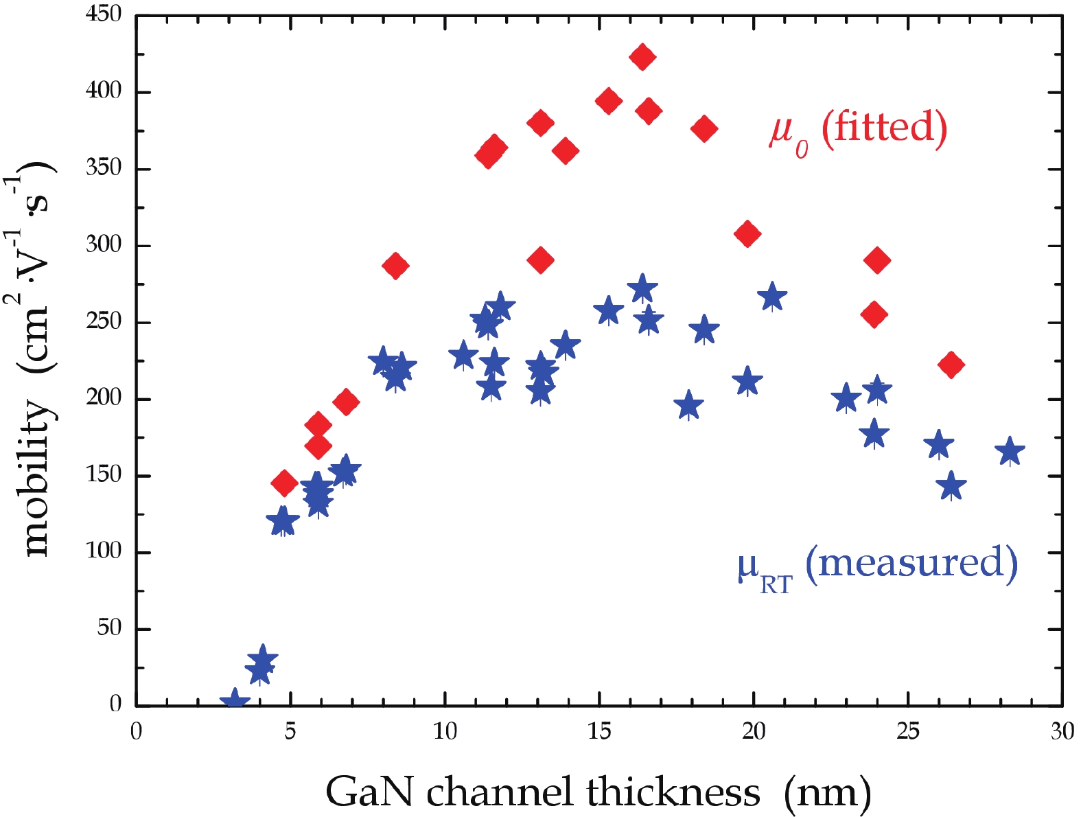
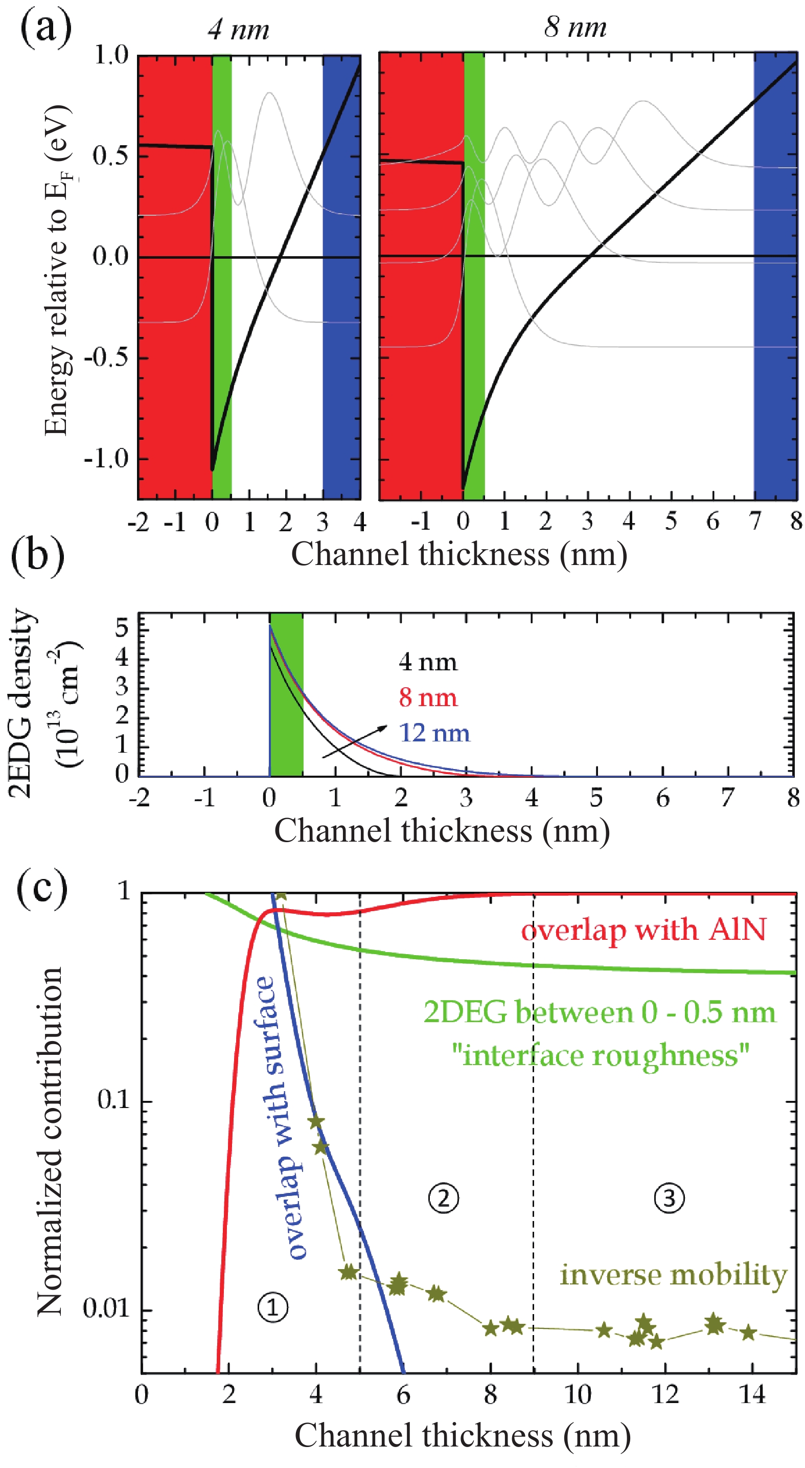
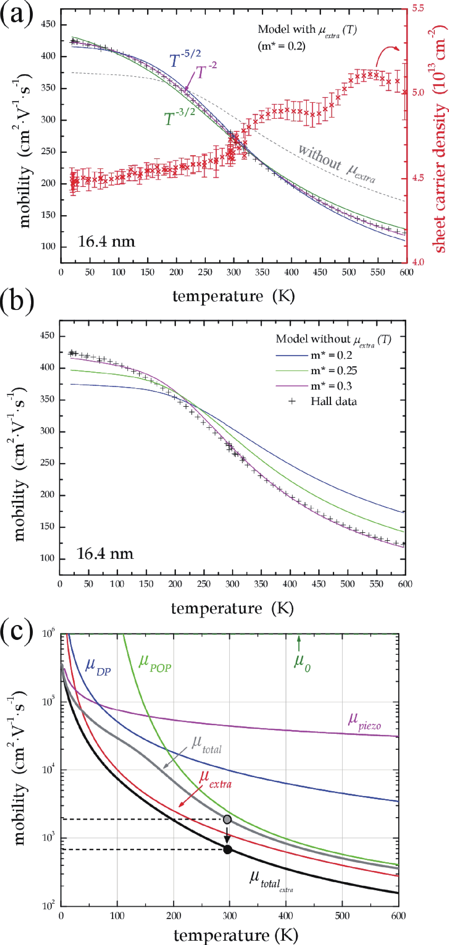
We have systematically studied the impact of thickness on the electrical properties of thin GaN channels on N-polar AlN (0001) templates grown on sapphire. The observed increase in sheet carrier density with increasing GaN thickness can be quantitatively reproduced by calculations assuming a Fermi-level pinning about 0.8 eV below the conduction band. The mobility strongly increases until 6 nm which correlates with reduced overlap of the 2DEG wave function with the surface layer. The mobility then increases more gradually up to 10 nm, corresponding to a reduced fraction of the 2DEG within the first 0.5 nm near the AlN/GaN interface, namely, the region affected by interface roughness. The mobility saturates at approximately 400 cm2·V−1·s−1, probably limited by dislocations and the overlap with deep traps inside the AlN back barrier. If the GaN thickness exceeds 15 nm, the mobility decreases, likely due to the onset of gradual relaxation and appearance of misfit dislocations. Finally, we note that the temperature-dependent mobility exhibits an unexpected contribution proportional to $ T^{-2} $ for all GaN channels on N-polar AlN, including those reported in the literature. Such observation may be explained by a 50% higher effective mass of the electron, which amplify the electron−phonon scattering, ultimately limiting the room-temperature mobility to about 750 cm2·V−1·s−1 and confining the sheet resistivity to values above 200 Ω/□.
J. Semicond.
2026, 47(7): 072502 doi: 10.1088/1674-4926/26030016
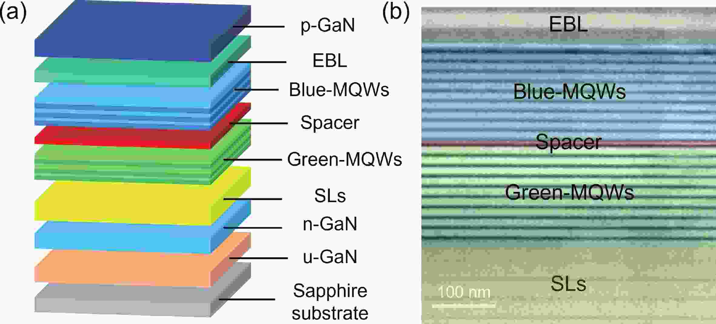
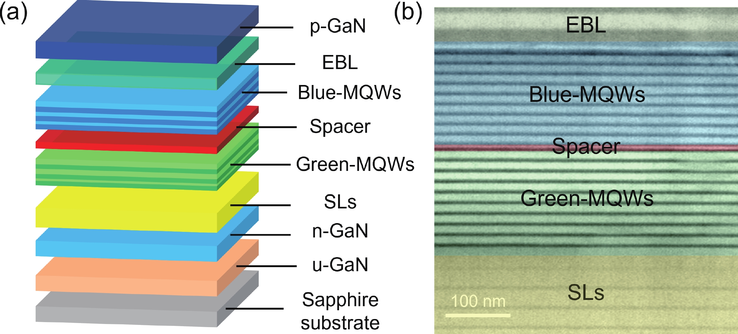
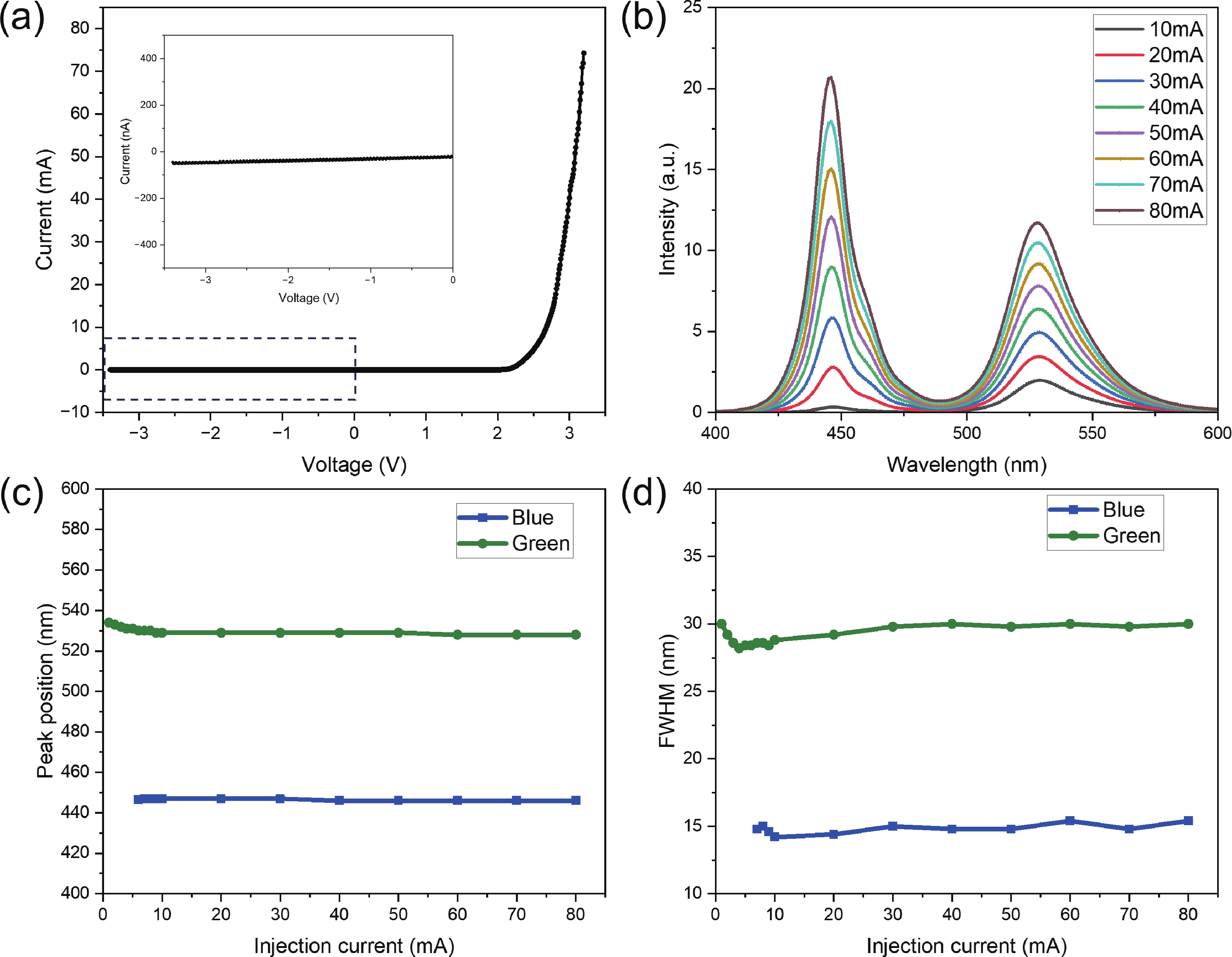
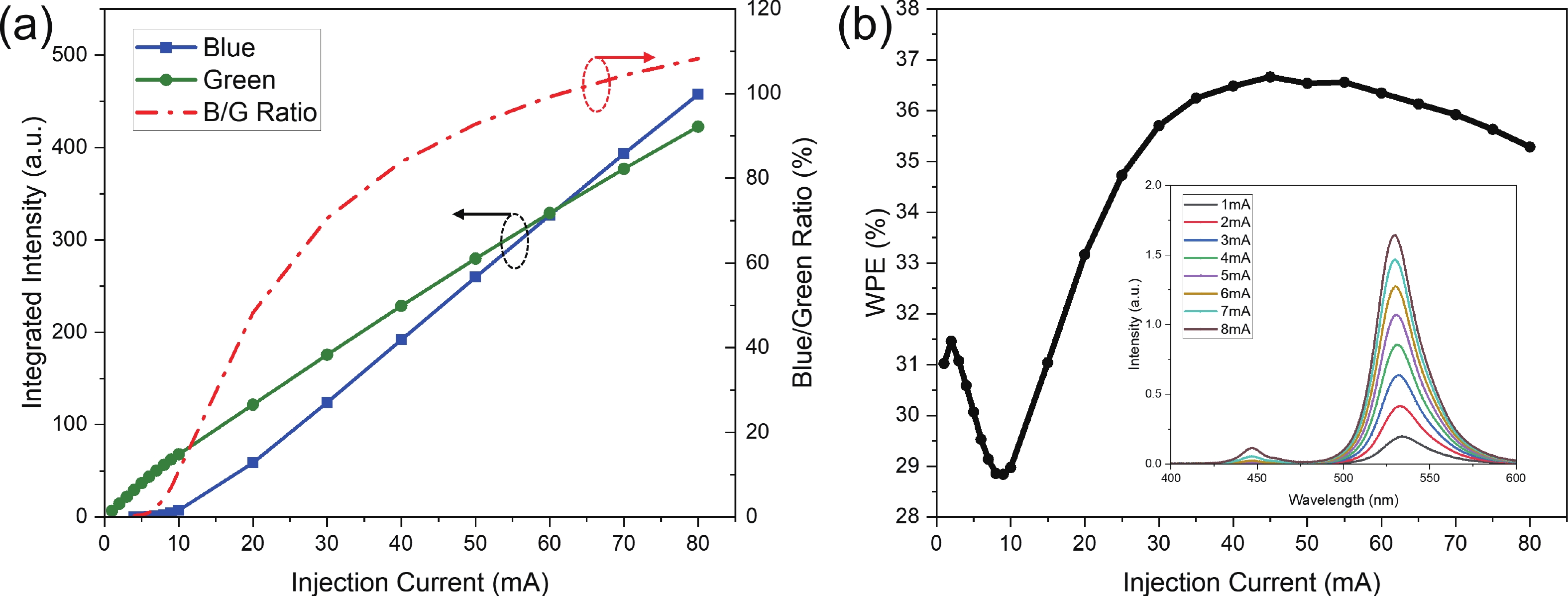
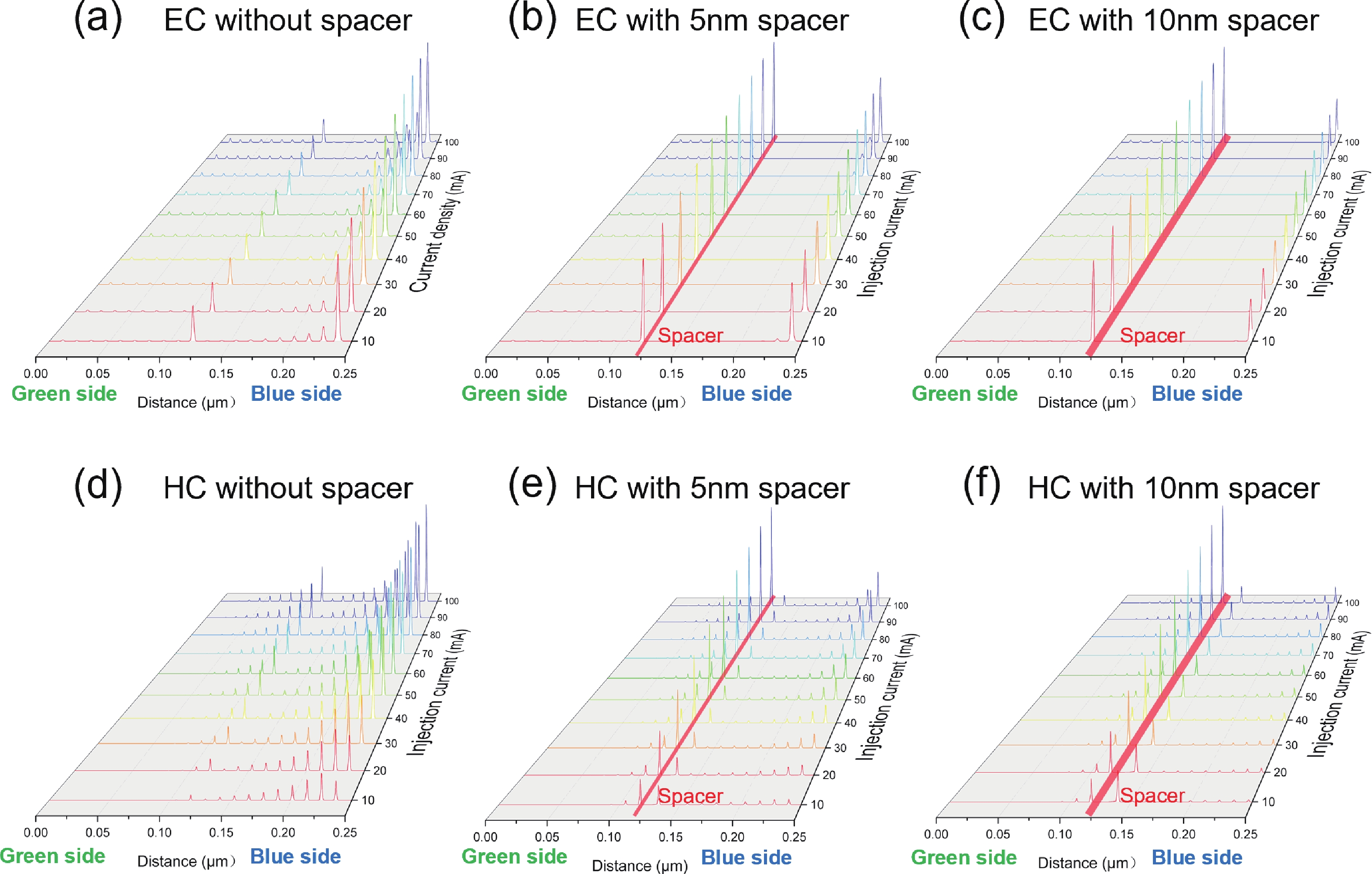
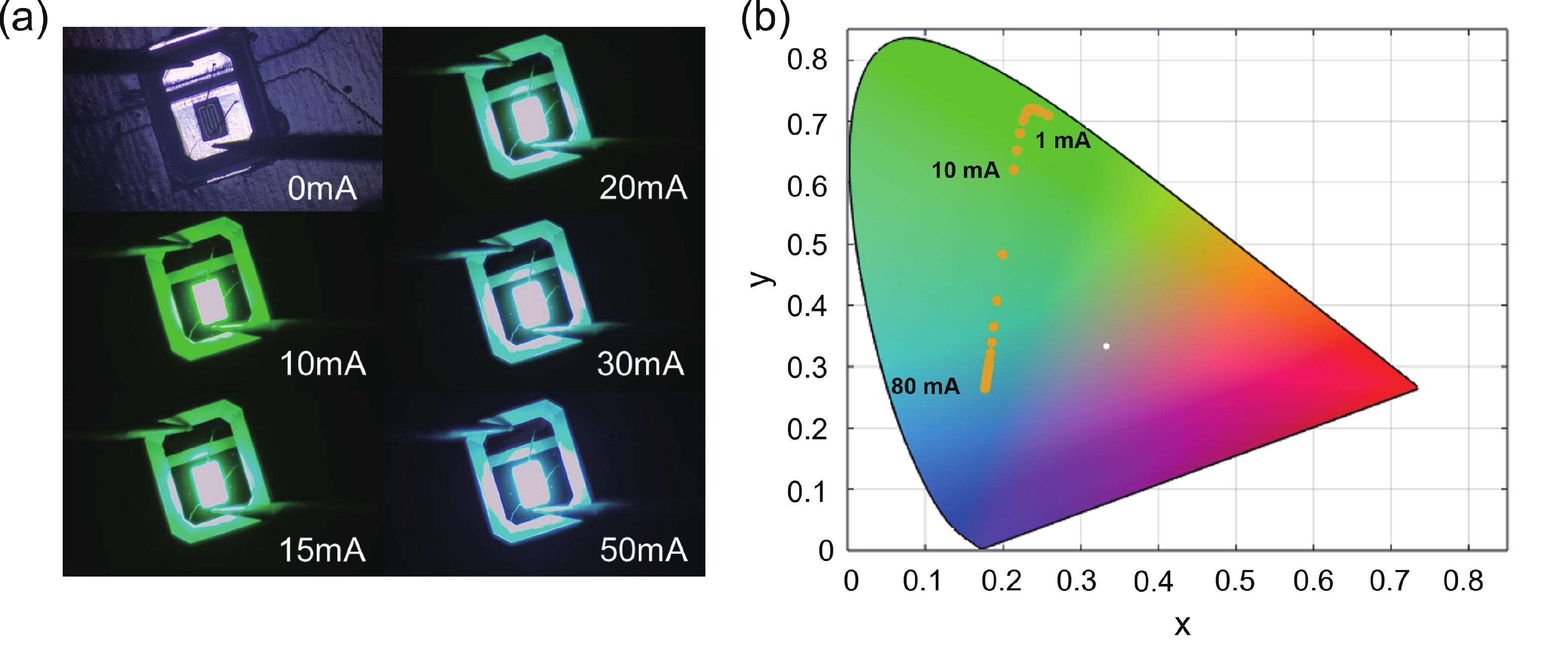
Ⅲ-nitride semiconductors with continuously tunable bandgaps are promising for white light emission and full-color displays. The mainstream RGB LED integration approach suffers from low long-wavelength efficiency and complex packaging. Herein, we demonstrate a novel single-chip dual-wavelength LED structure, which integrates blue (upper) and green (bottom) multiple quantum wells (MQWs) separated by a GaN intermediate spacer layer. The device exhibits two distinct emission peaks at 446 and 528 nm, with excellent luminescence stability. We investigate the role of the spacer layer and reveal its critical effect on the carrier distribution and radiative recombination behavior. The maximum wall-plug efficiency (WPE) of the device reaches approximately 36.7%, and its abnormal droop curve indicates a transition of the green emission mechanism from electroluminescence (EL) to photoluminescence (PL). By tuning the injection current, the dual-wavelength LED achieves a continuous color transition from green to blue, which corresponds to chromaticity coordinates ranging from (0.2584, 0.7098) to (0.1771, 0.2649) in the CIE 1931 chromaticity diagram. This work provides a feasible and flexible strategy for emission color modulation, and also lays a foundation for the development of high-performance solid-state lighting devices.
J. Semicond.
2026, 47(7): 072503 doi: 10.1088/1674-4926/26010043
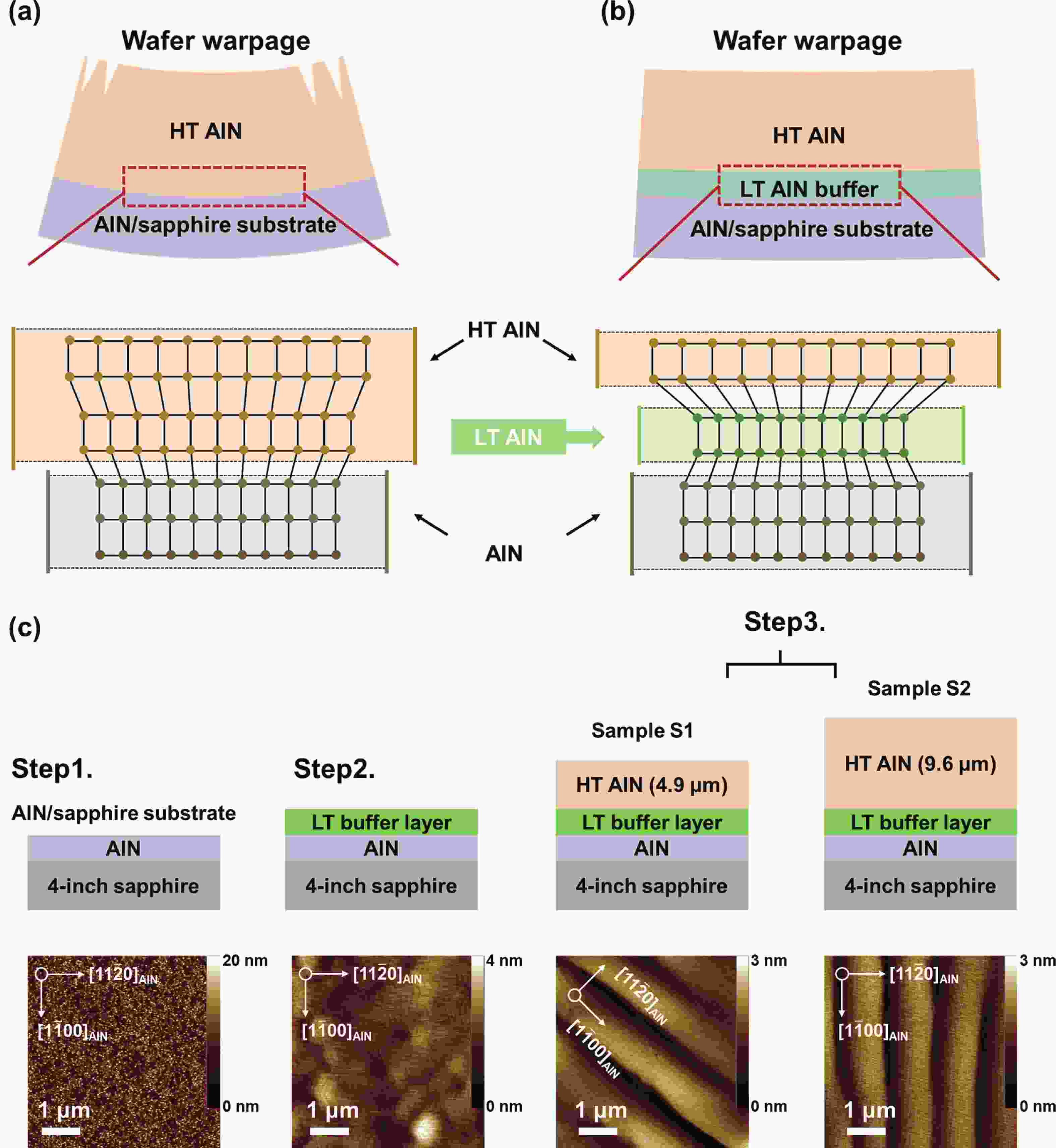
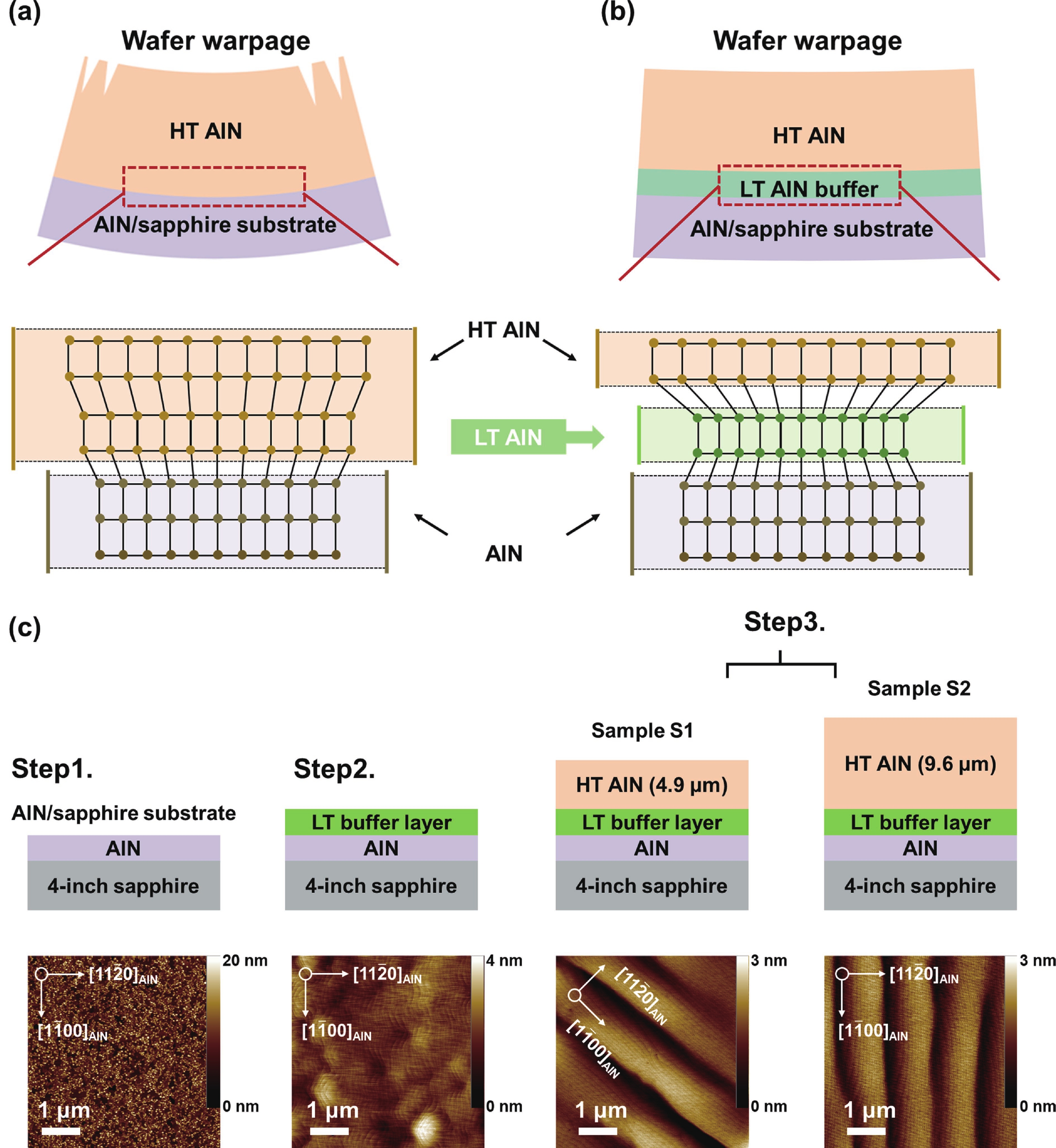
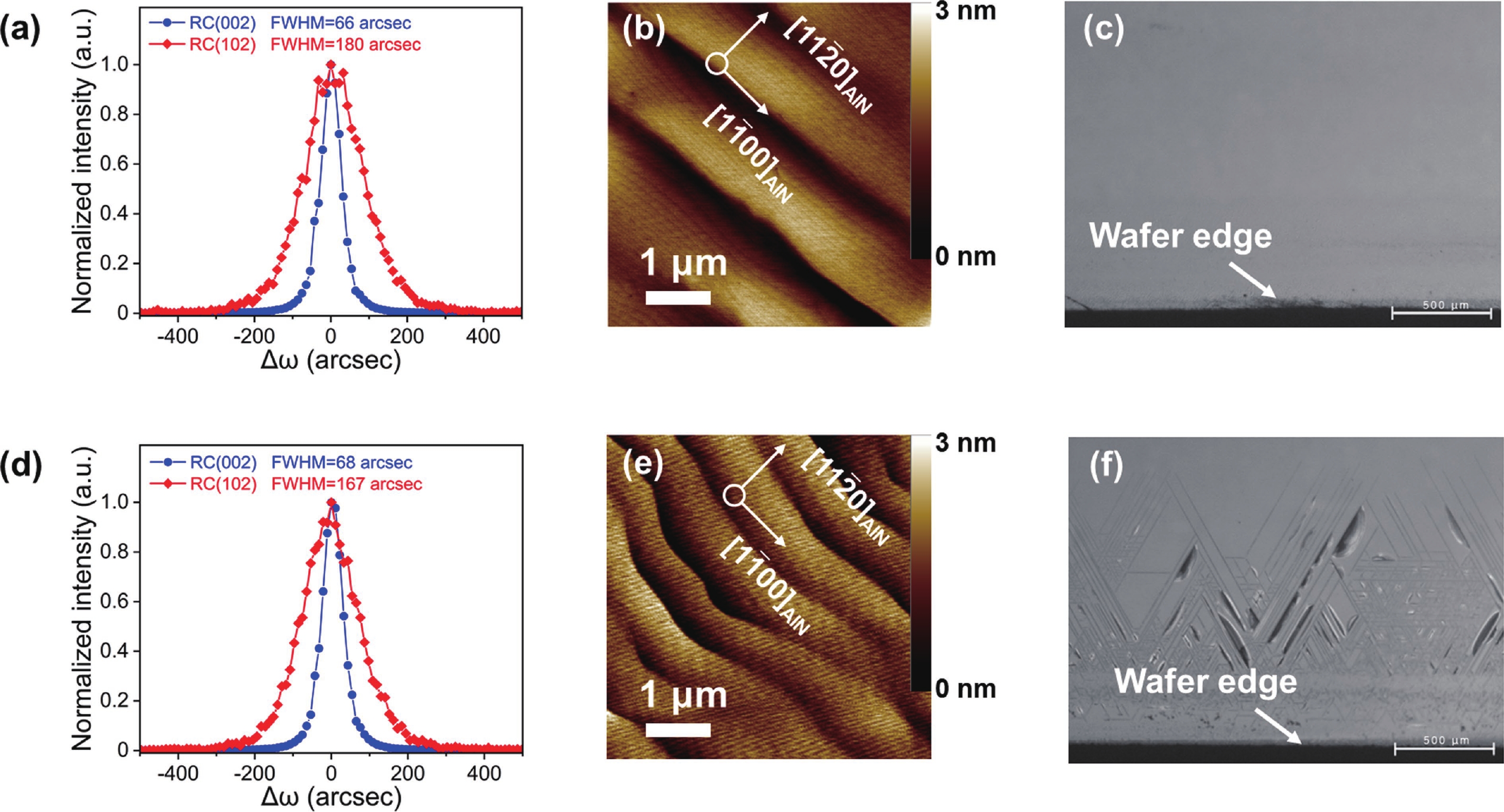
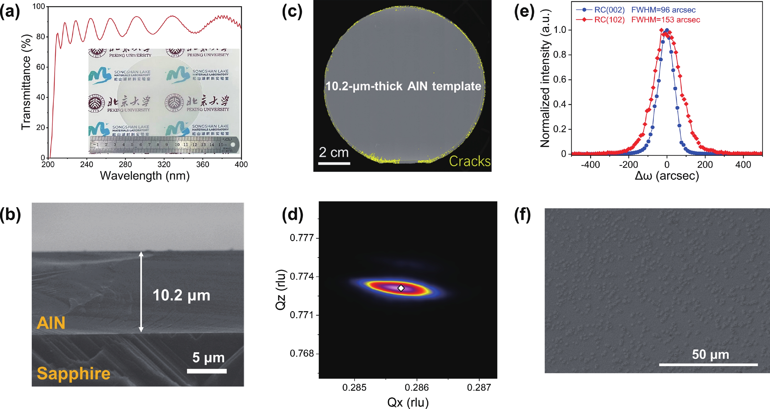
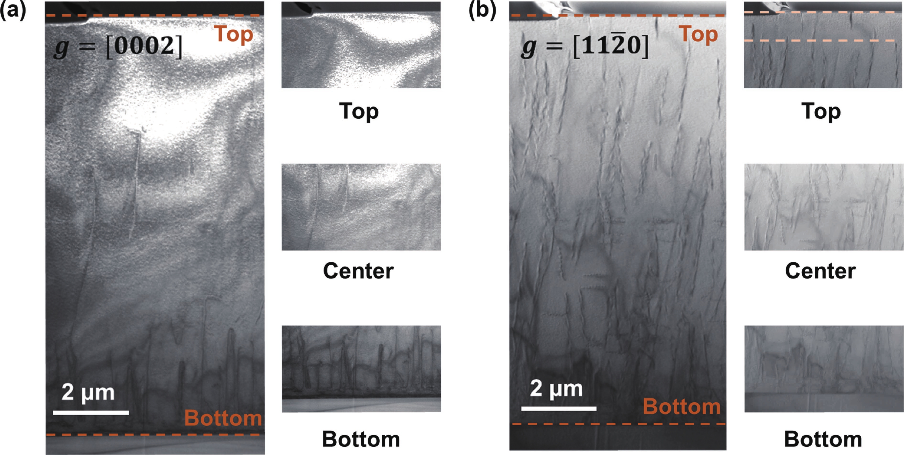
Achieving aluminum nitride (AlN) epilayers with dislocation densities below 107 cm−2 on sapphire remains critical for ultraviolet (UV) optoelectronics applications. However, the lattice and thermal mismatches inherent to heteroepitaxial growth hinder the simultaneous suppression of threading dislocations and surface cracking. In this work, a 10.2-μm-thick, 4-inch AlN film was fabricated on an AlN/sapphire substrate. A strain-modulated buffer was embedded beneath the AlN epilayer to pre-introduce a well-balanced compressive strain, which counteracted tensile strain accumulation during thick-layer growth while maintaining continuous two-dimensional epitaxy for effective defect suppression. This strain management strategy, combined with progressive dislocation annihilation as the layer thickness increased, yielded a surface dislocation density of 7.6 × 106 cm−2 and limited cracking to within approximately 2 mm from the wafer edge. This scalable and cost-effective approach enables the growth of crack-suppressed, high-quality AlN epilayers on sapphire, offering a practical pathway for UV optoelectronic devices in light of the current limitations of bulk AlN substrates.
J. Semicond.
2026, 47(7): 072504 doi: 10.1088/1674-4926/26020066
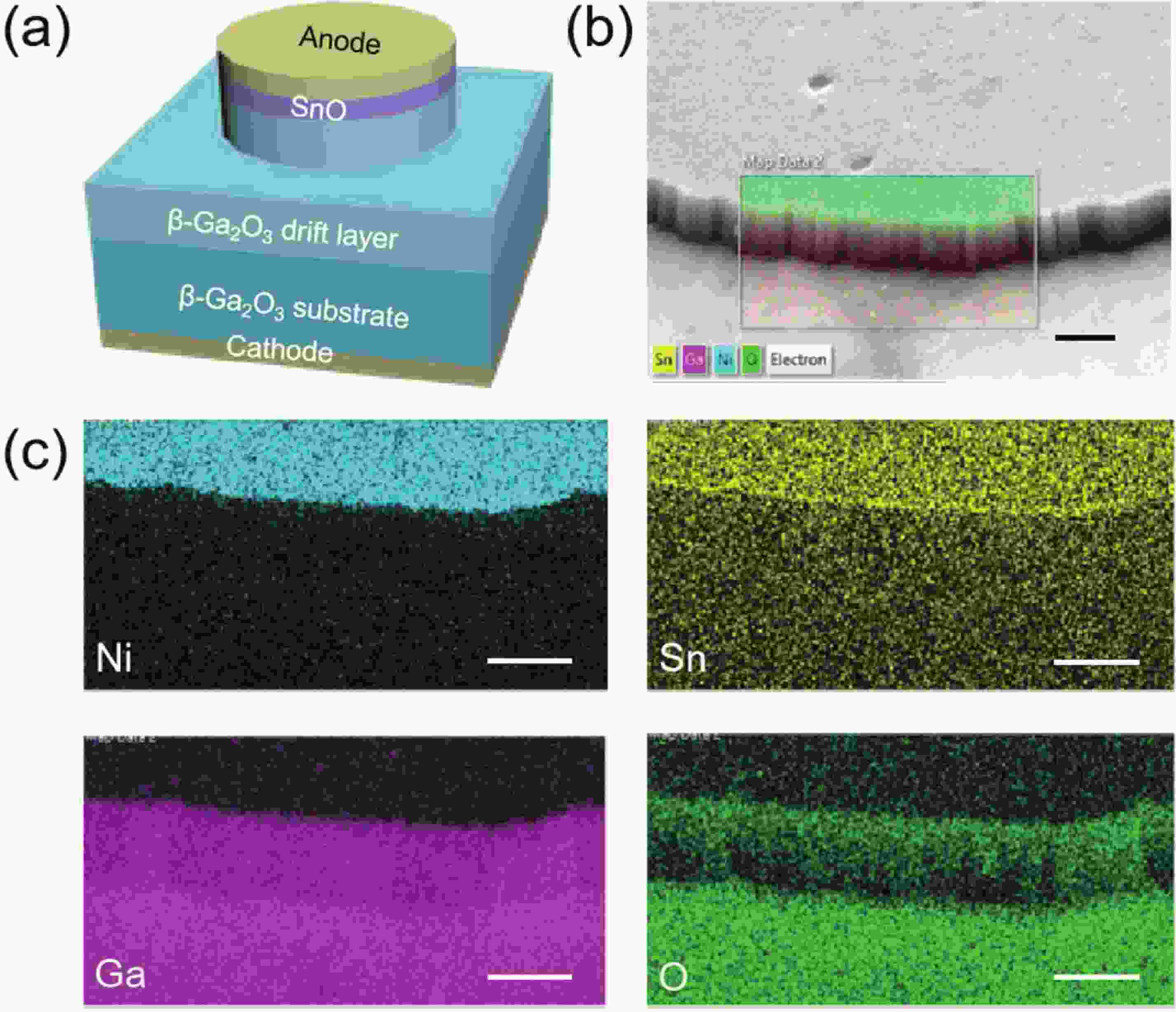
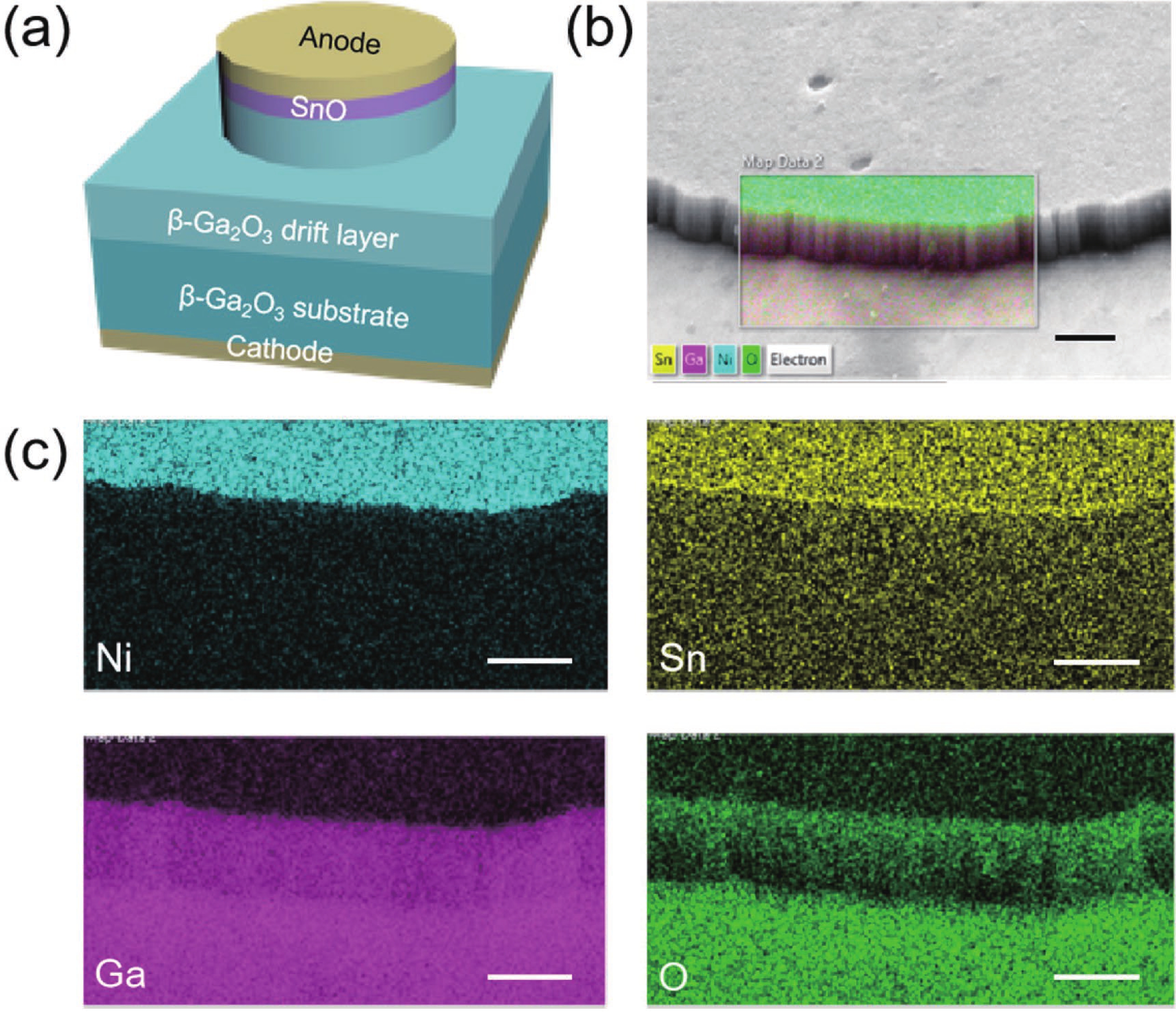
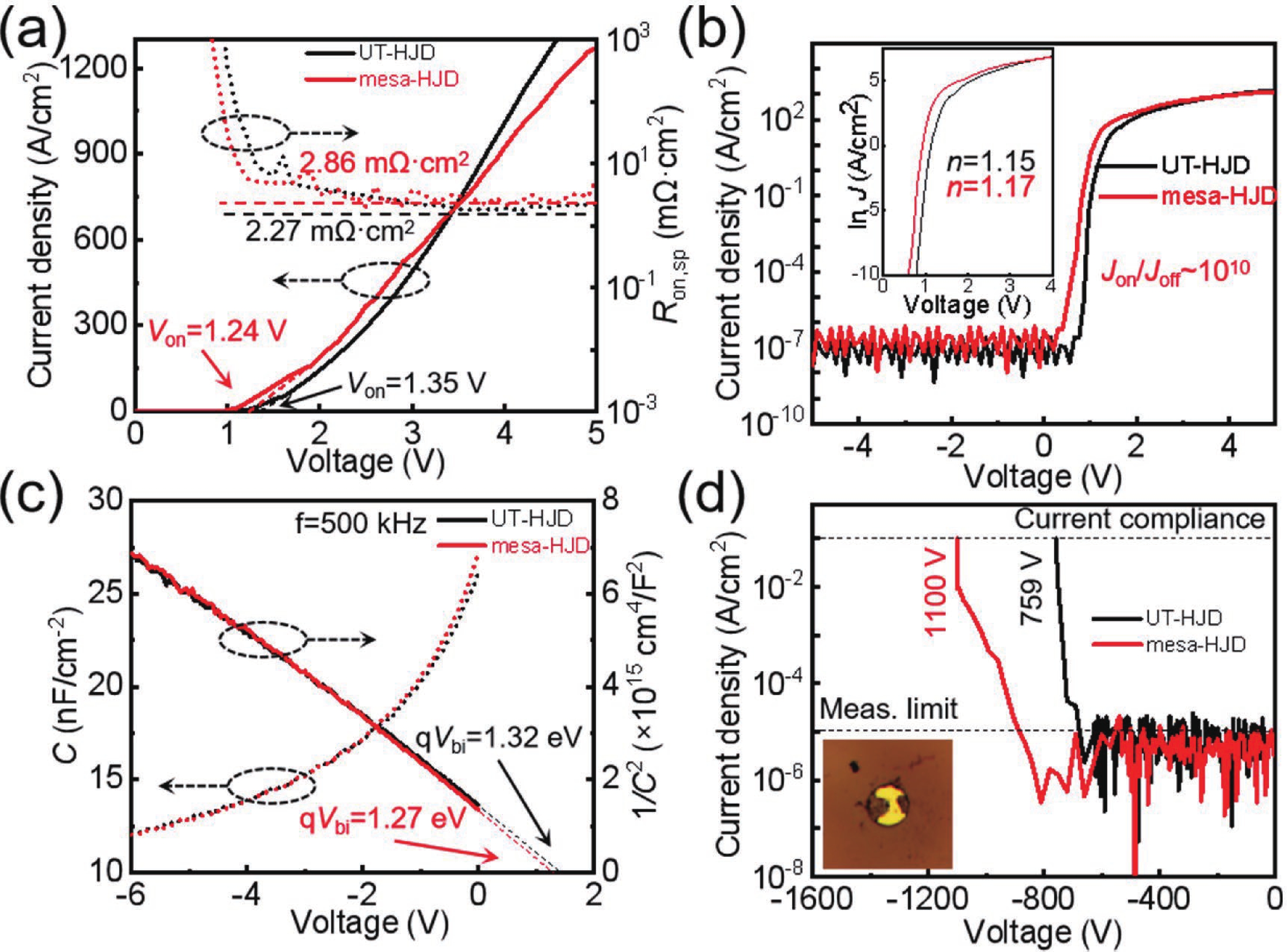
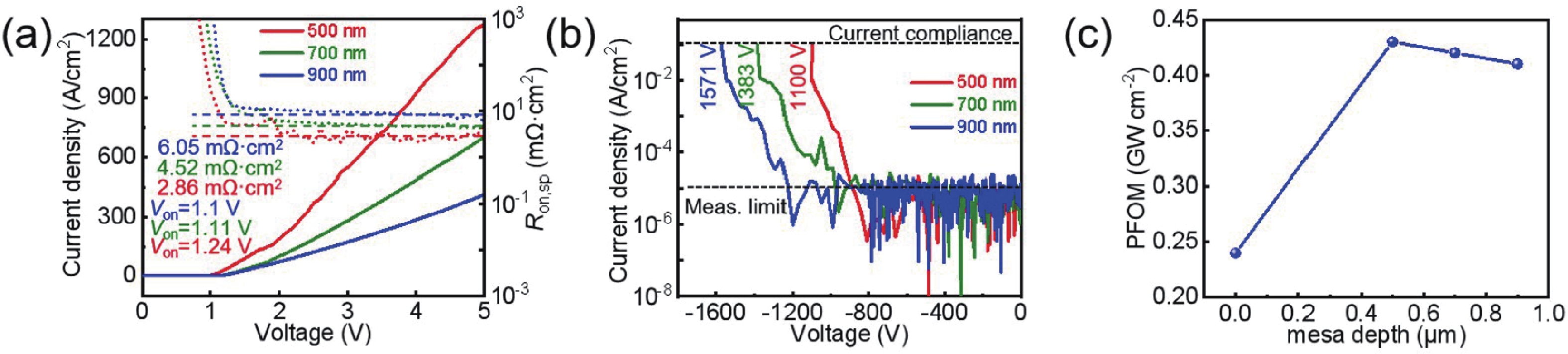
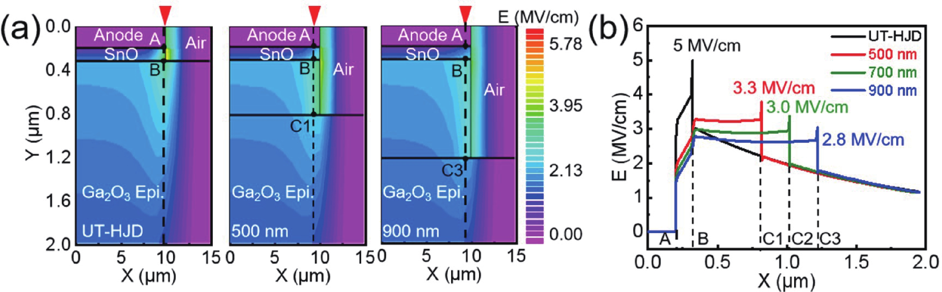
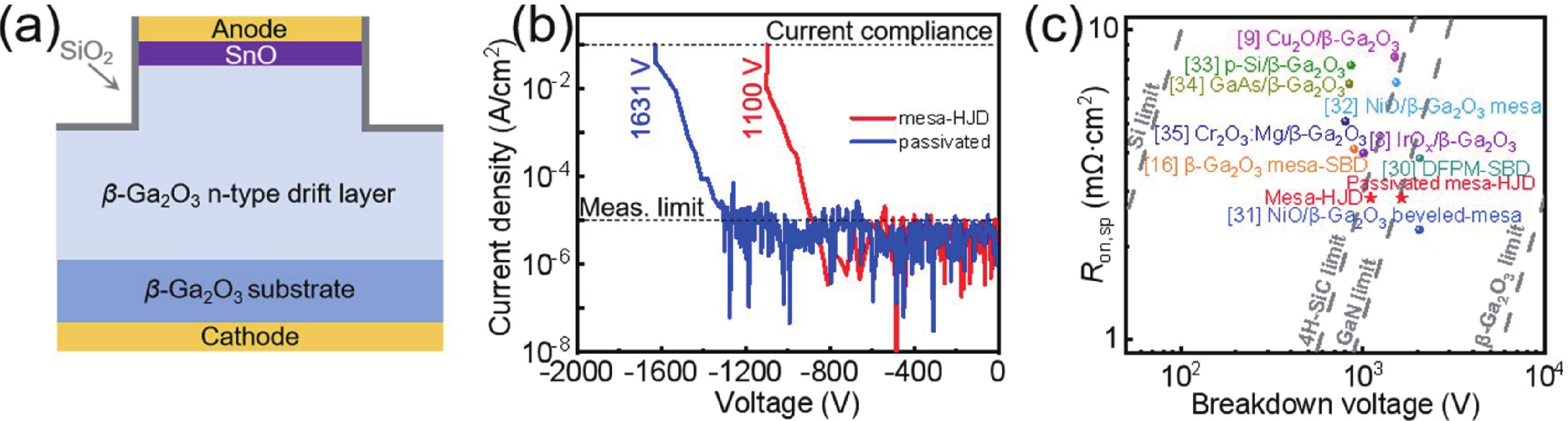
In this article, a vertical SnO/β-Ga2O3 mesa heterojunction diode (mesa-HJD) fabricated through self-aligned etching is reported. The mesa structure eliminates the influence of lateral depletion at the region, leading to an improved breakdown characteristics in comparison with its unterminated heterojunction diode (UT-HJD) counterpart. The SnO/β-Ga2O3 mesa-HJD, featuring a 500 nm mesa depth, achieves a breakdown voltage (BV) of 1100 V, which can be improved to 1631 V by sidewall passivation. With the increase of mesa depth, BV increases, accompanied by the increase of specific on-resistance (Ron,sp). Therefore, a maximum Baliga’s power figure of merit (PFOM) can be achieved for the optimized device with 500 nm mesa depth, giving the value of 0.93 GW/cm2 for the passivated device. The mesa-HJD demonstrates considerable potential for application in high BV β-Ga2O3 power electronic devices in the future.
J. Semicond.
2026, 47(7): 072701 doi: 10.1088/1674-4926/26010032
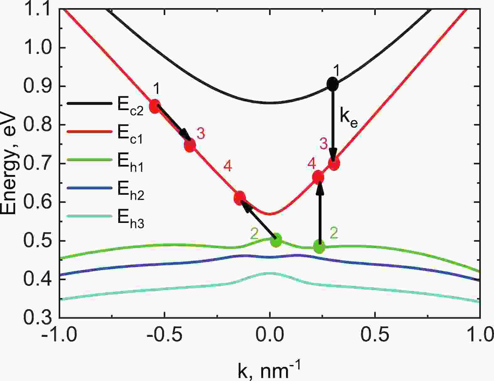
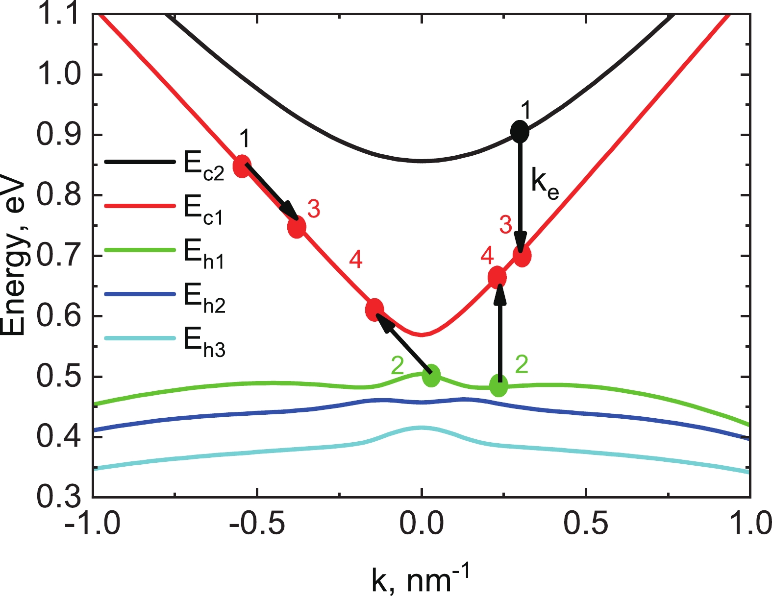
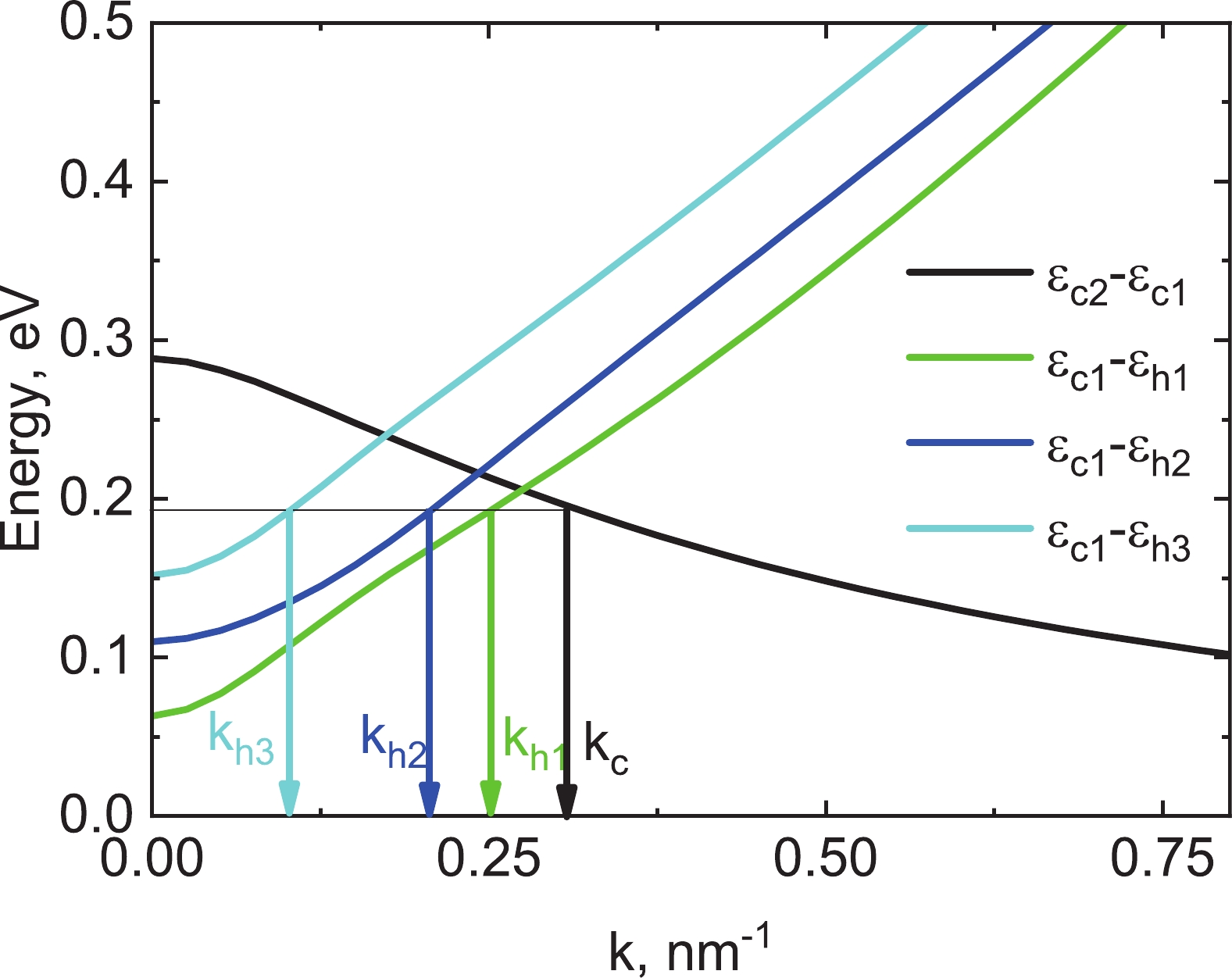
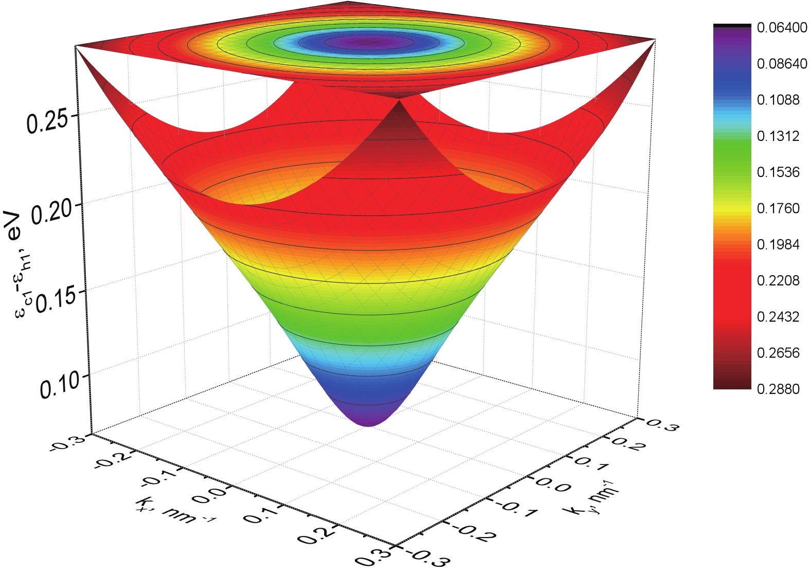
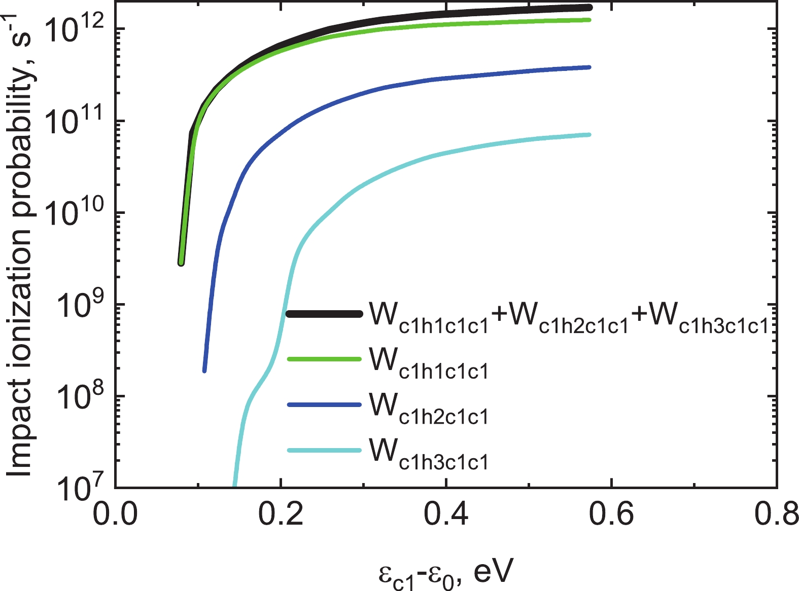
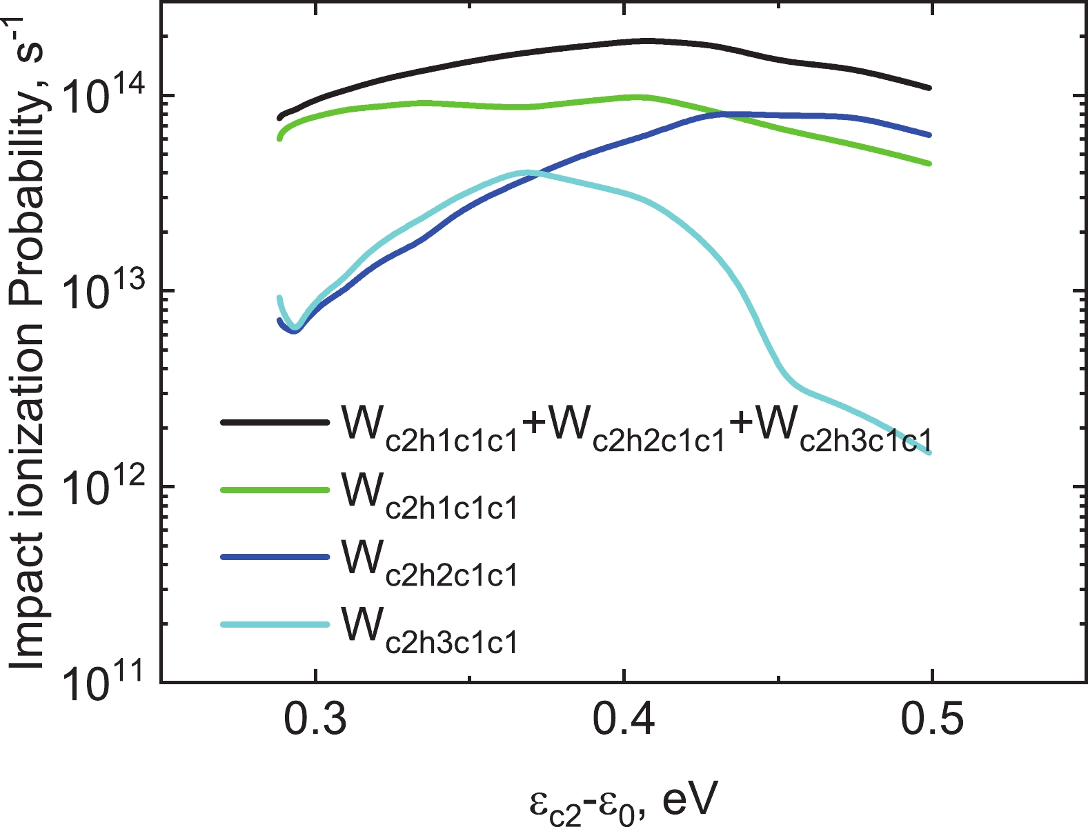
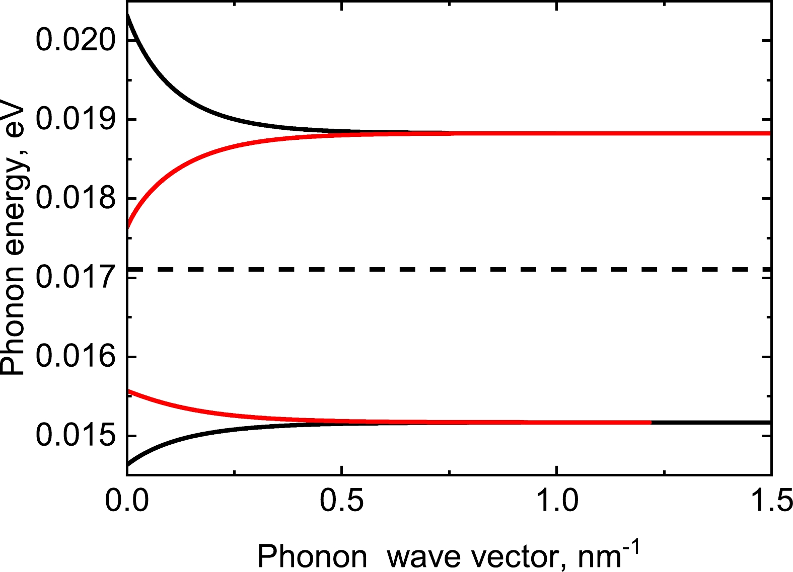
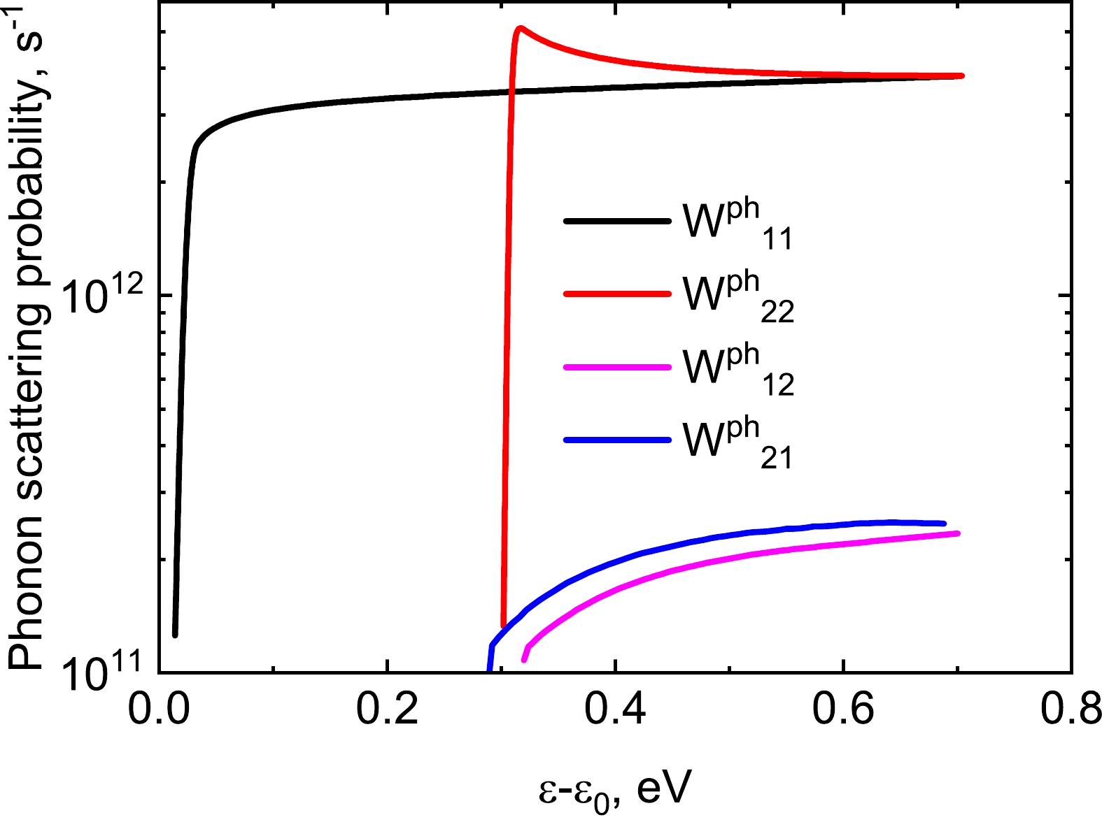
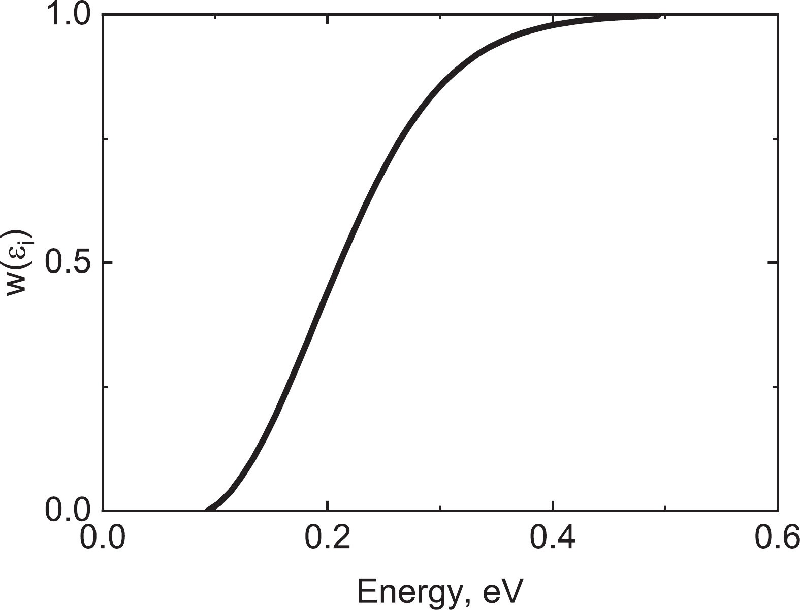
Impact ionization probabilities were calculated in a CdHgTe quantum well, where the distance between electron subbands is close to the band gap energy. This band structure enables impact ionization with small momentum transfer for electrons in the second subband. The study demonstrates that such processes increase the impact ionization probability by approximately two orders of magnitude compared to the impact ionization probability for electrons in the first subband, for which transitions with small momentum changes are impossible. The probability of single impact ionization during the electron energy loss due to optical phonon emission is estimated. Experimental methods for detecting impact ionization in this structure are discussed.
J. Semicond.
2026, 47(7): 072702 doi: 10.1088/1674-4926/26010009
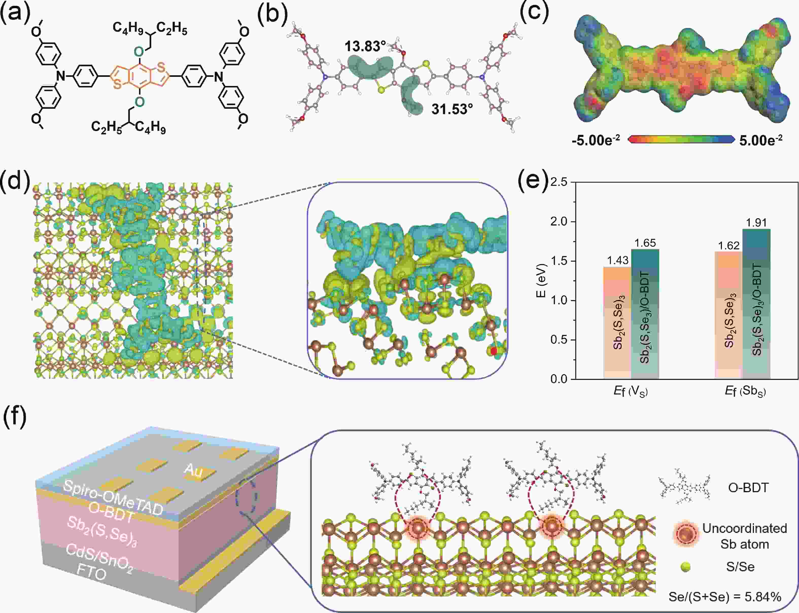
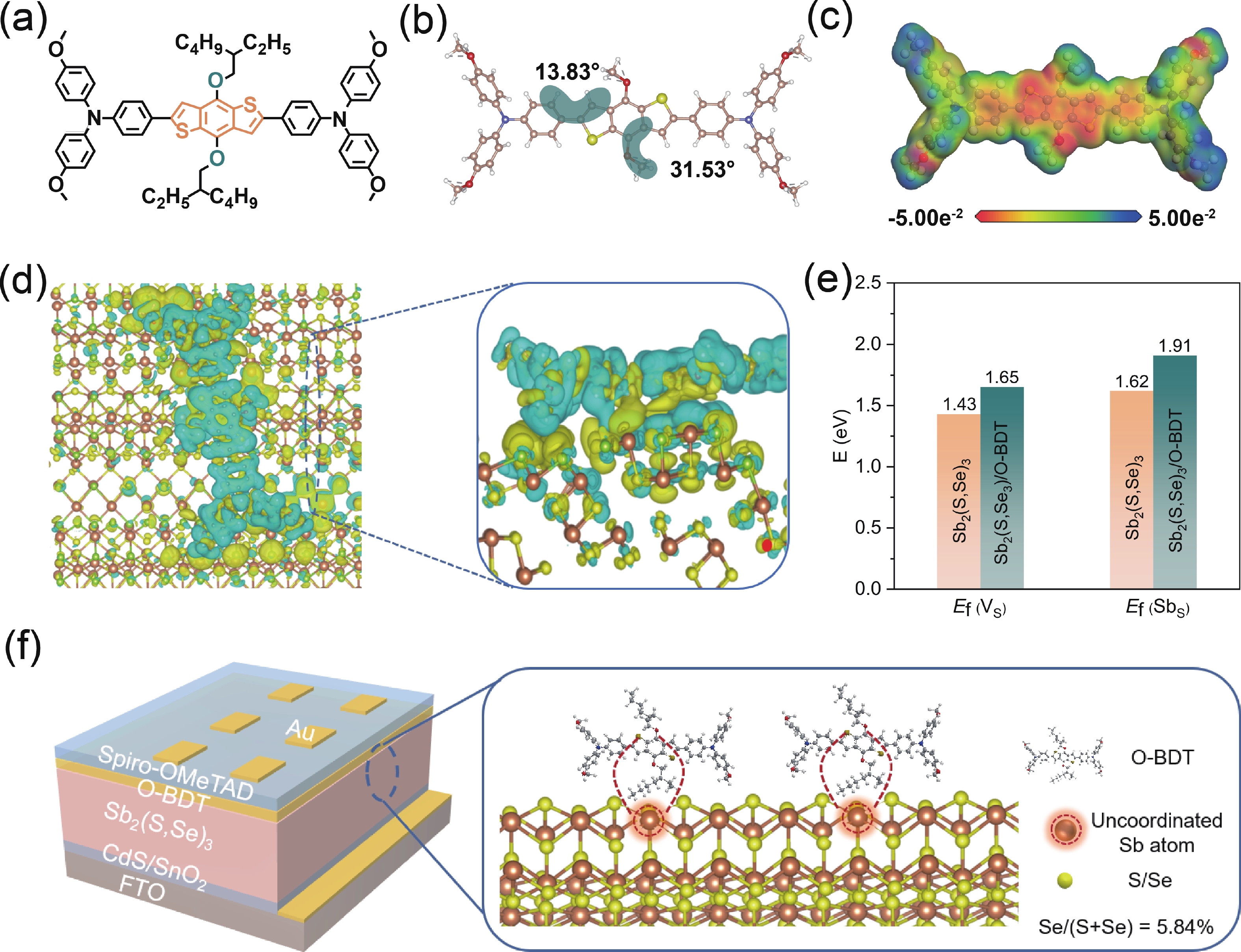
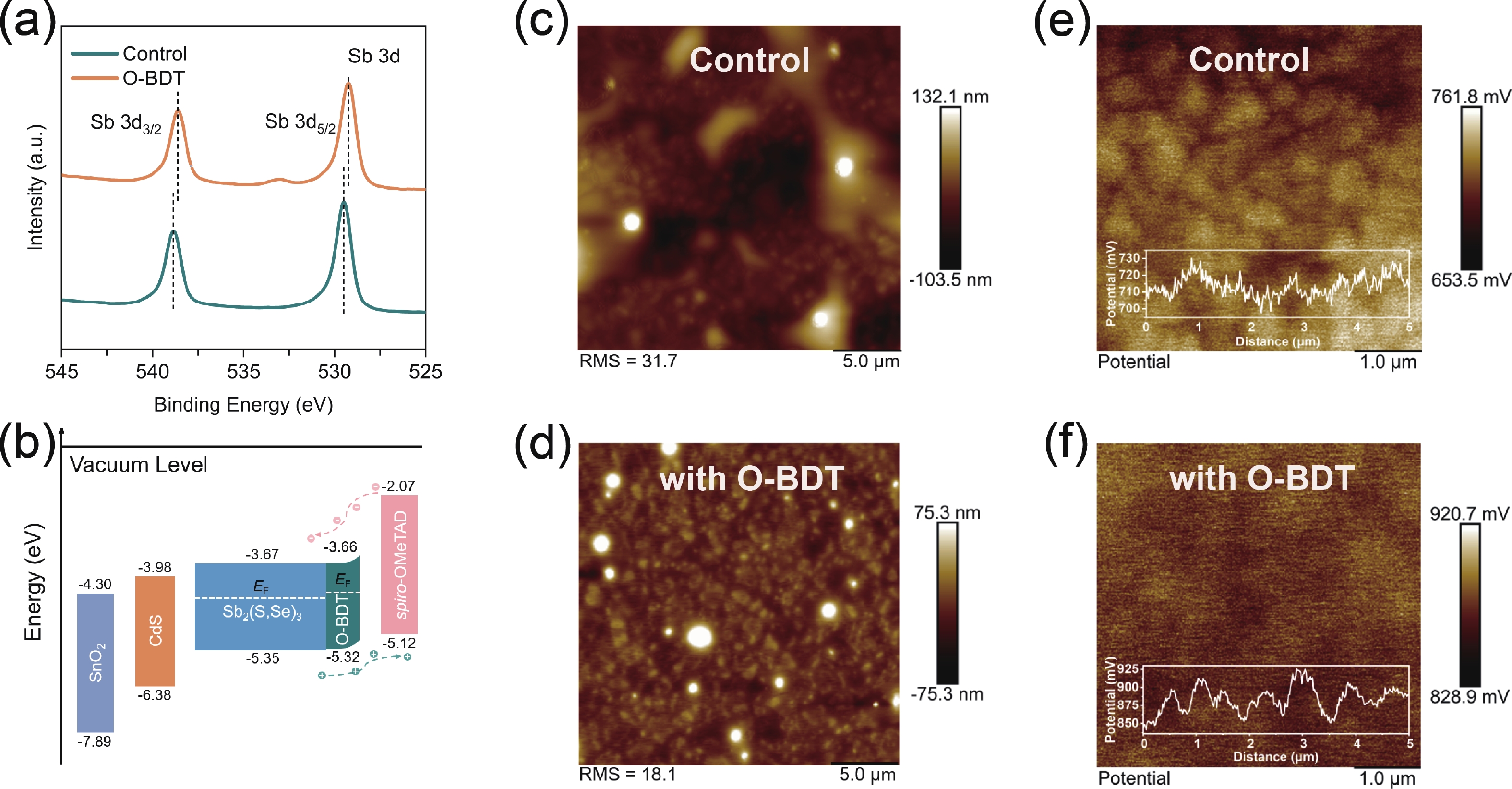
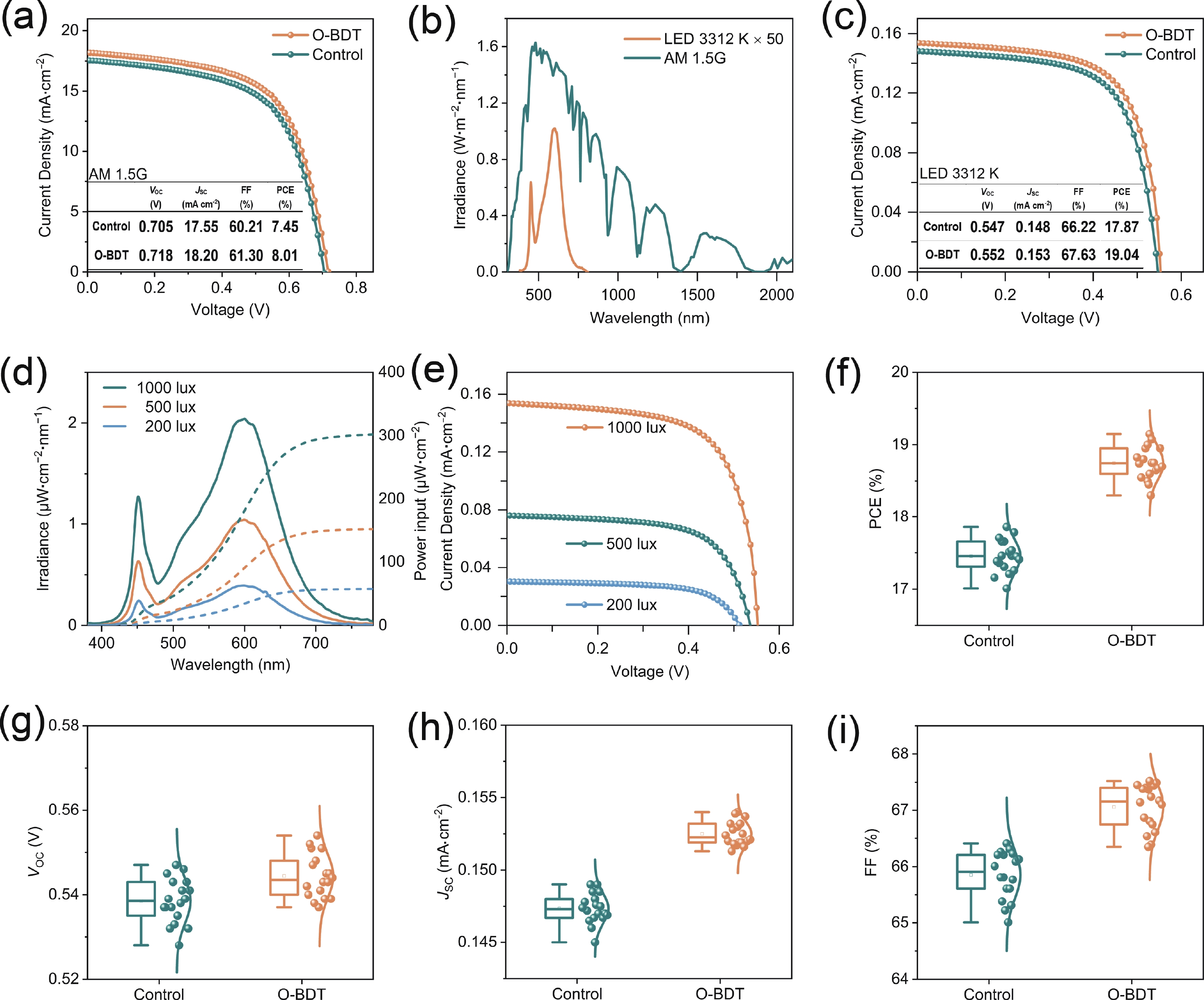
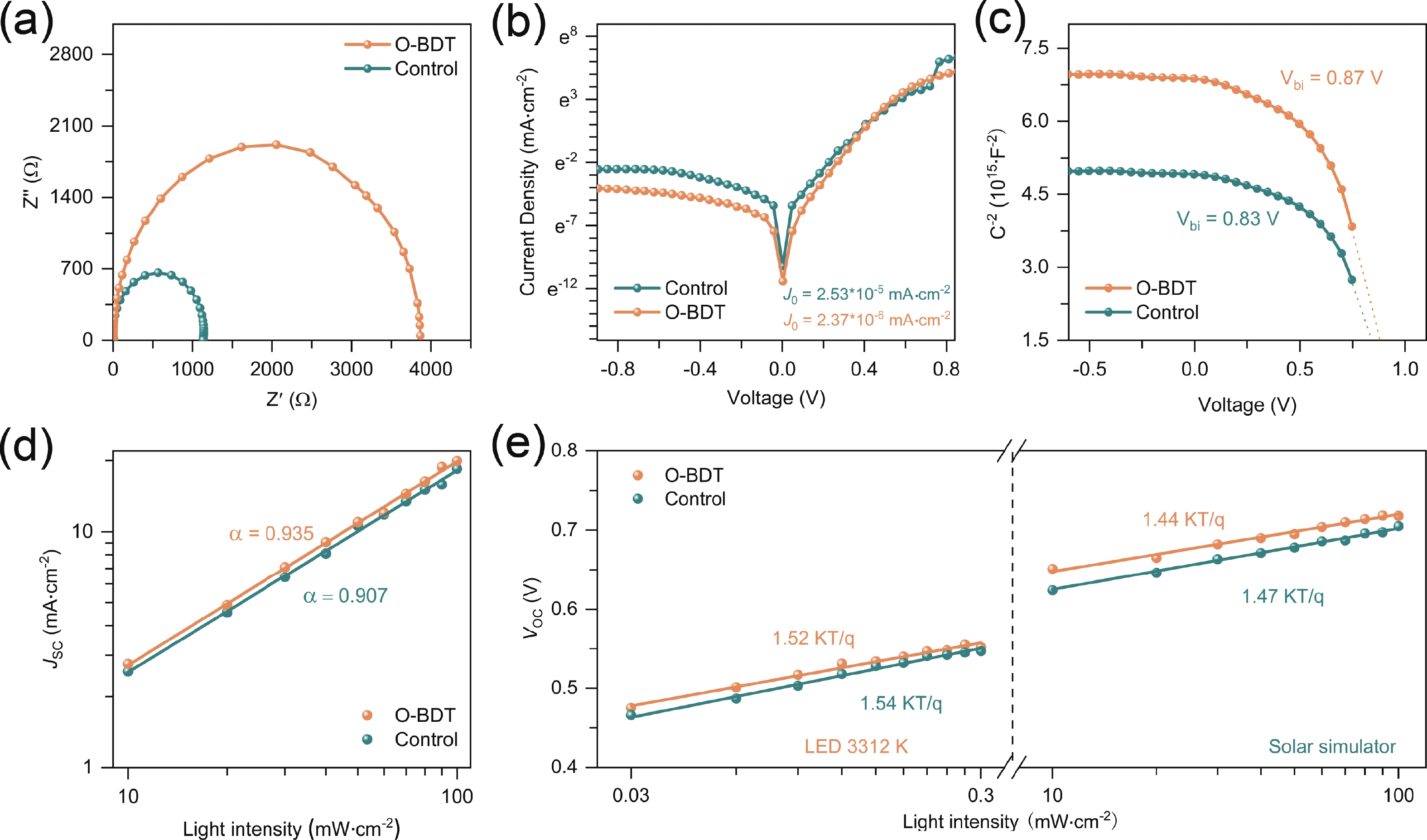
Antimony selenosulfide (Sb2(S,Se)3) is a promising photovoltaic absorber material for both outdoor and indoor application scenarios. Nevertheless, the performance of Sb2(S,Se)3 solar cells remains constrained by the severe interface trap-induced nonradiative recombination. Interface engineering has been recognized as an effective approach to suppress recombination and boost charge transport. In this work, we introduce an organic modifier (O-BDT) between Sb2(S,Se)3 absorber and hole transport layer. The theoretical and experimental results evidence that O-BDT can simultaneously passivates interface defects and optimizes the energy-level alignment, leading to a significantly reduced voltage loss. Finally, the O-BDT modified solar cell achieves a power conversion efficiency (PCE) of 8.01% under AM 1.5G illumination. Moreover, the device delivers a PCE of 19.04% under 1000 lux, 3312 K LED lighting, among the best list of IPVs based on antimony chalcogenide compounds.
J. Semicond.
2026, 47(7): 072801 doi: 10.1088/1674-4926/26040046

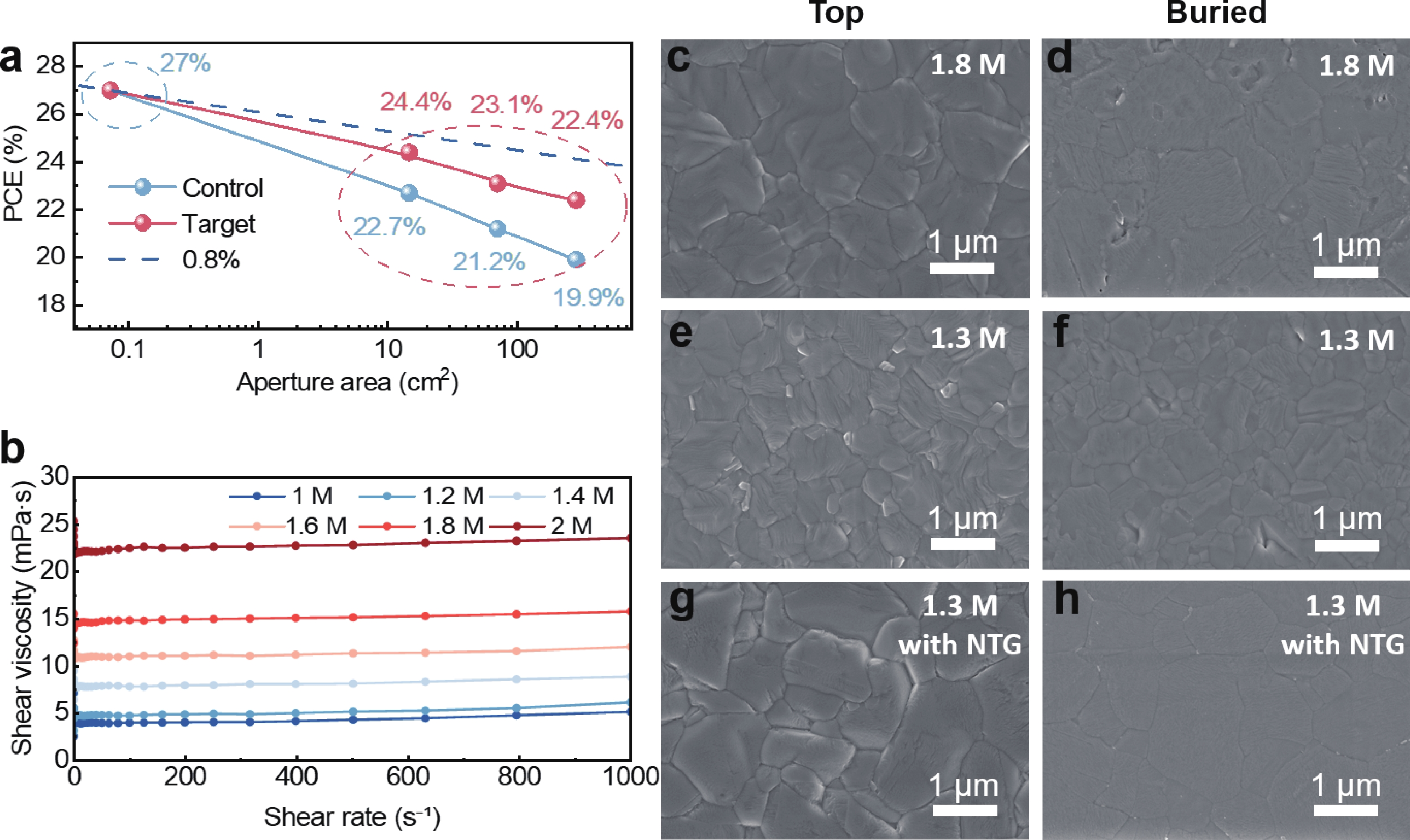
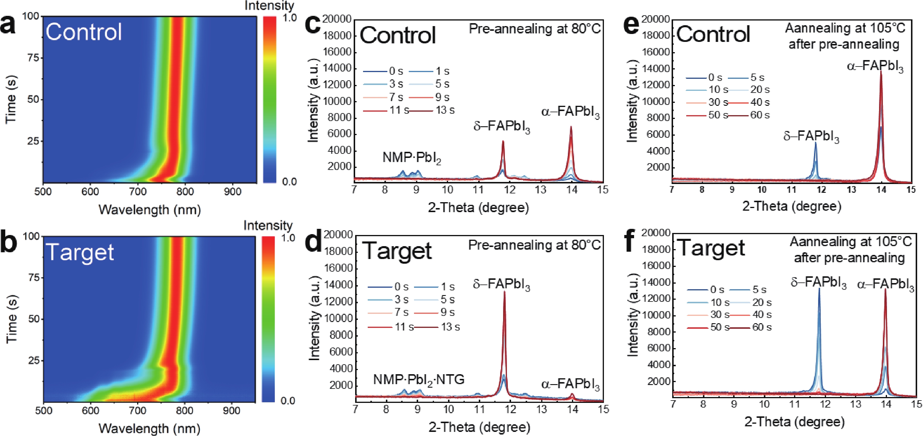
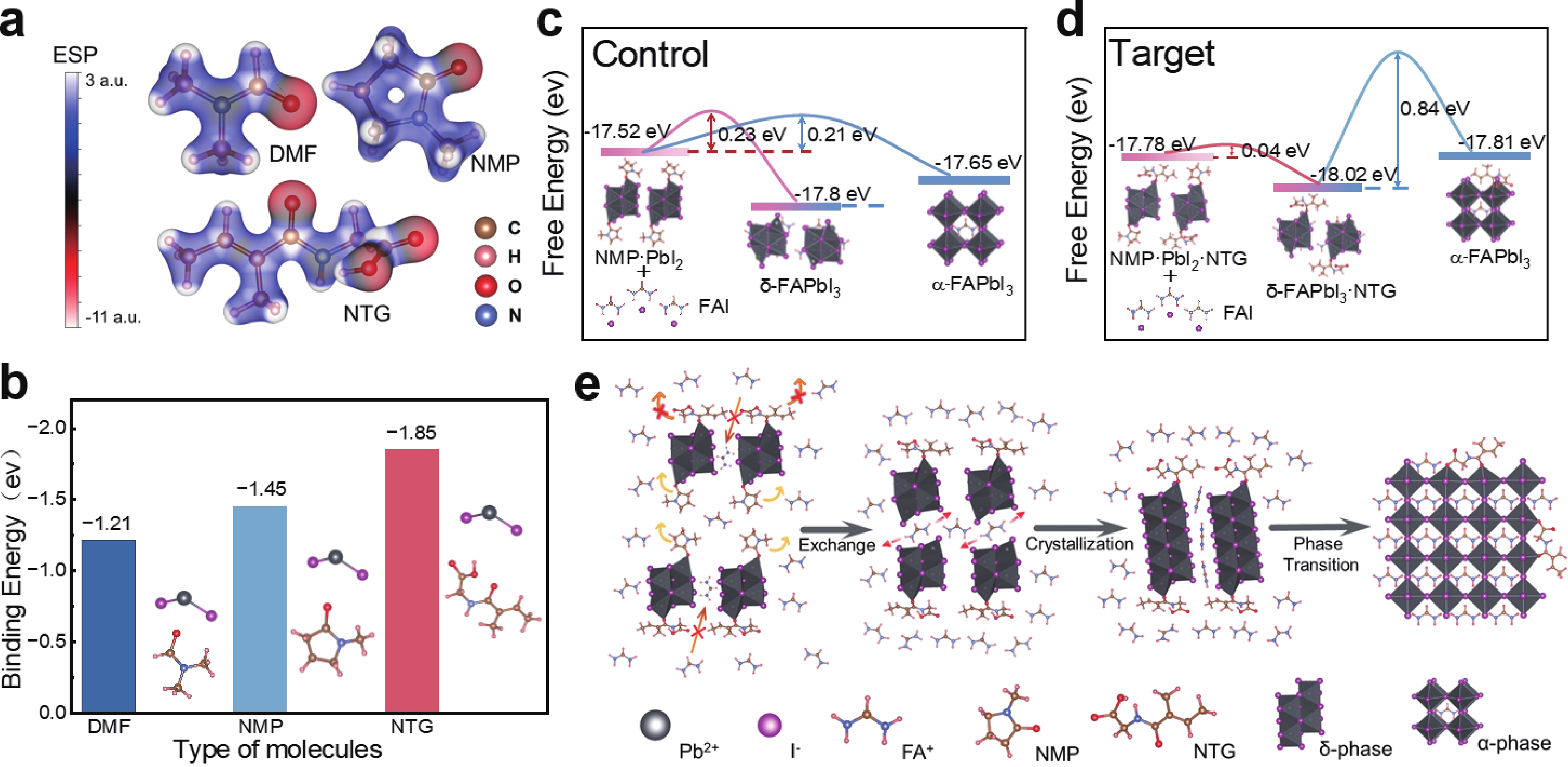
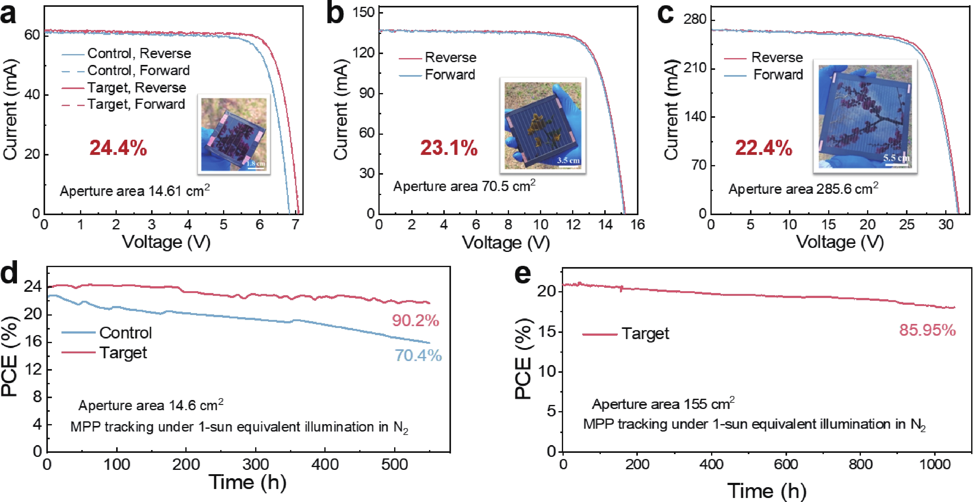
Large-area perovskite solar cell modules efficiency remains lower than small-area devices, perovskite crystallization between small and large areas difference could be one reason. Previously, diluted solution was often used to reduce viscosity to achieve uniform perovskite thin films, but this approach could narrow the crystallization window and leave insufficient time for controlled crystal growth. Meanwhile, insufficient solute supply often results in interrupted material availability for grain growth, leading to the formation of excessive small crystal nuclei and thus poor thin-film quality. Here, we developed a strategy that use a bi-functional group additive to stabilize the δ-FAPbI3 intermediate phase, which delays the direct and rapid conversion of lead iodide into α-FAPbI3 during large-area perovskite film growth. Based on this strategy, the efficiencies of perovskite modules with aperture areas of 14.6, 70.5, and 285.6 cm2 developed in this work are 24.4% (certified steady-state efficiency: 24.4%), 23.1%, and 22.4%, respectively. The efficiency loss per order-of-magnitude increase in area was reduced from 2.0% to 1.3%, which is approaching the state of the art of traditional thin-film CdTe solar cells (0.8%). In addition, the large-area module (155 cm2) retained 86% of its initial efficiency after 1053 h of maximum power point (MPP) tracking.