Issue Browser
Volume 47, Issue 6,
Jun 2026
J. Semicond.
2026, 47(6): 062201 doi: 10.1088/1674-4926/25120027
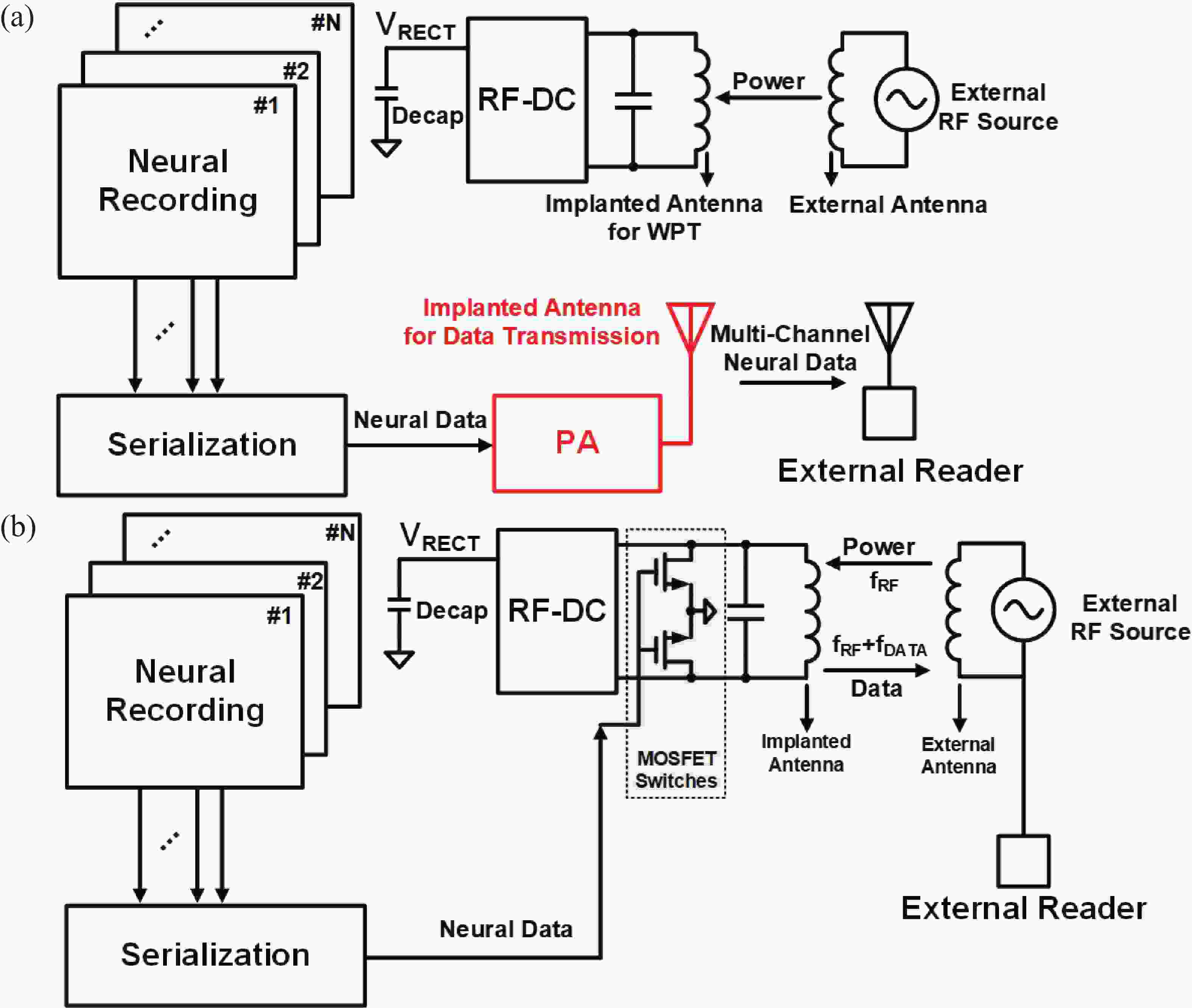
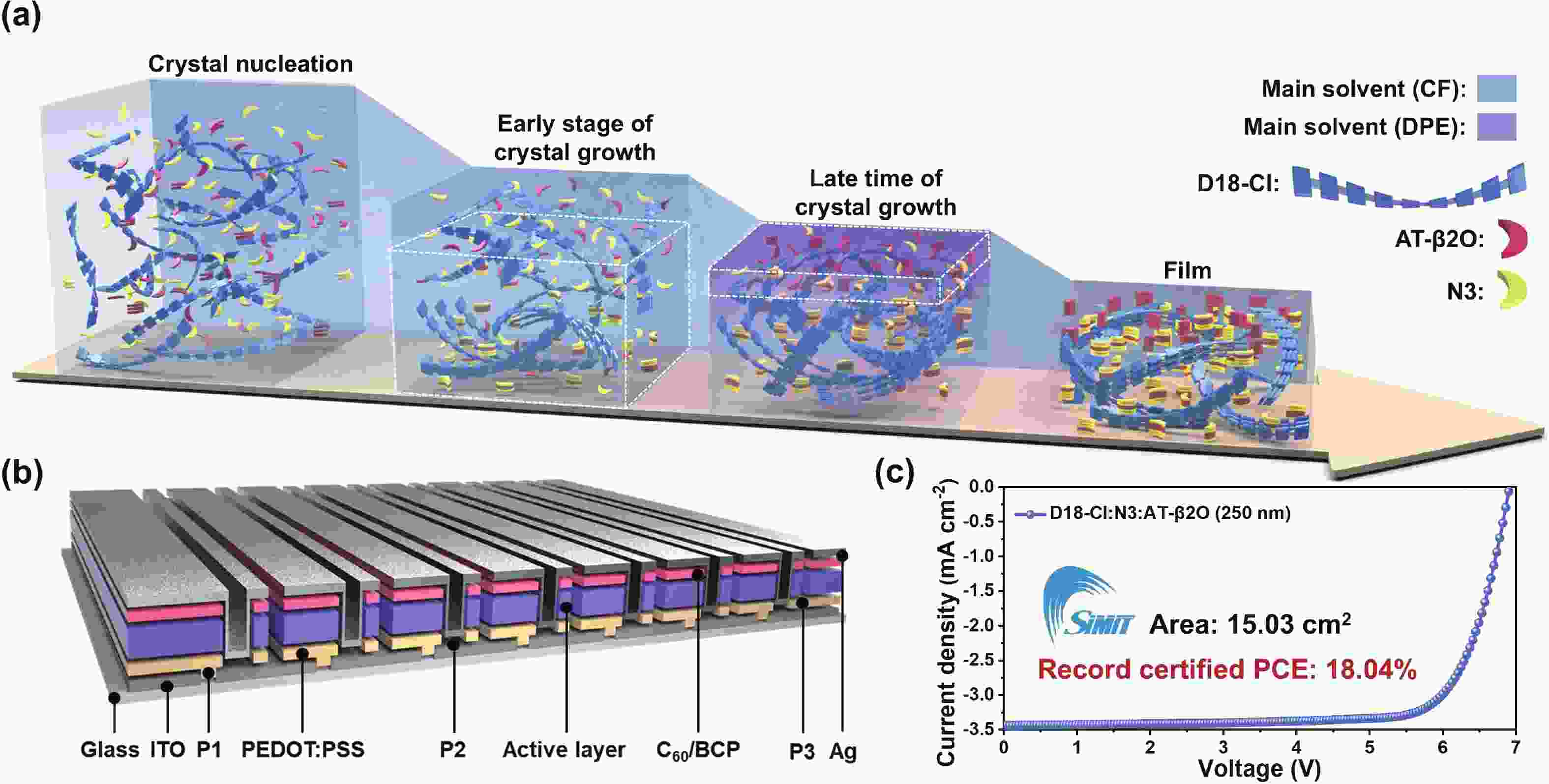
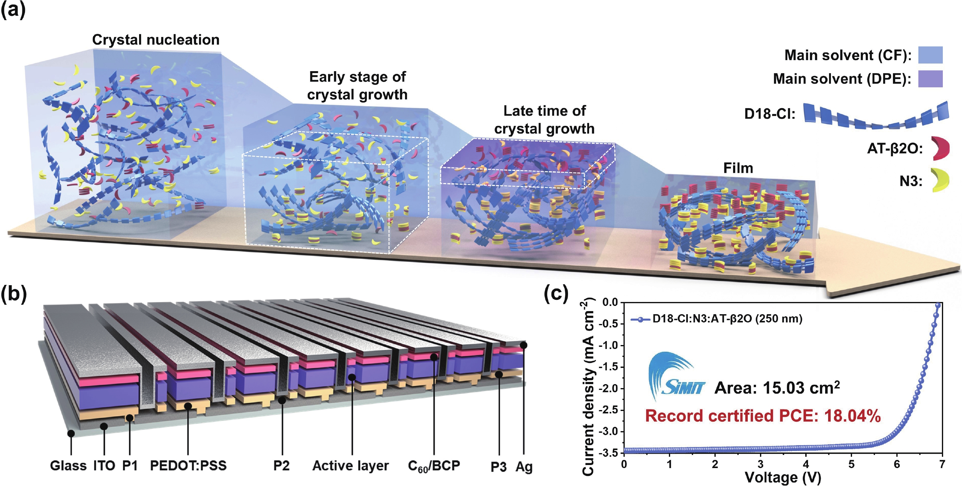
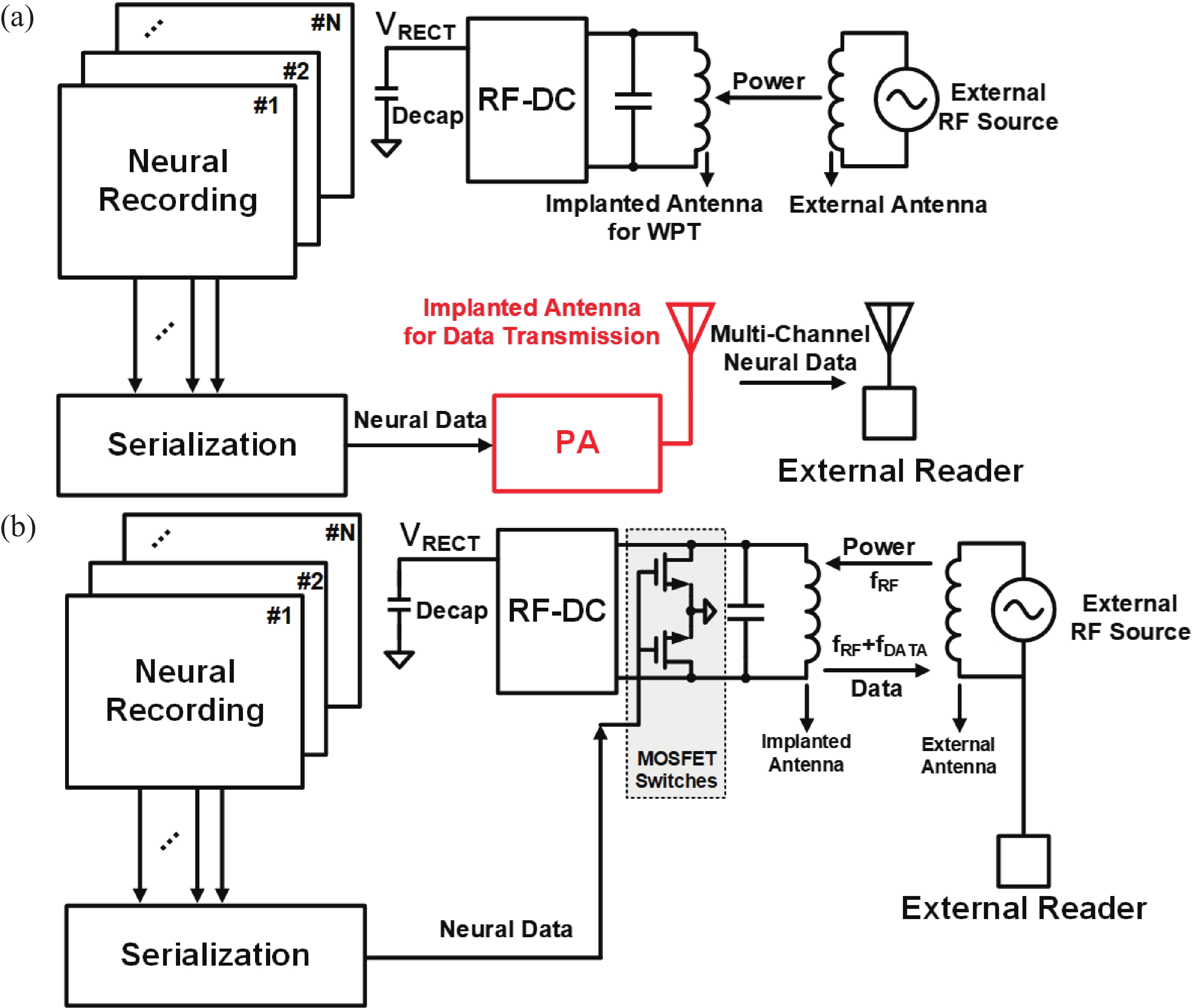
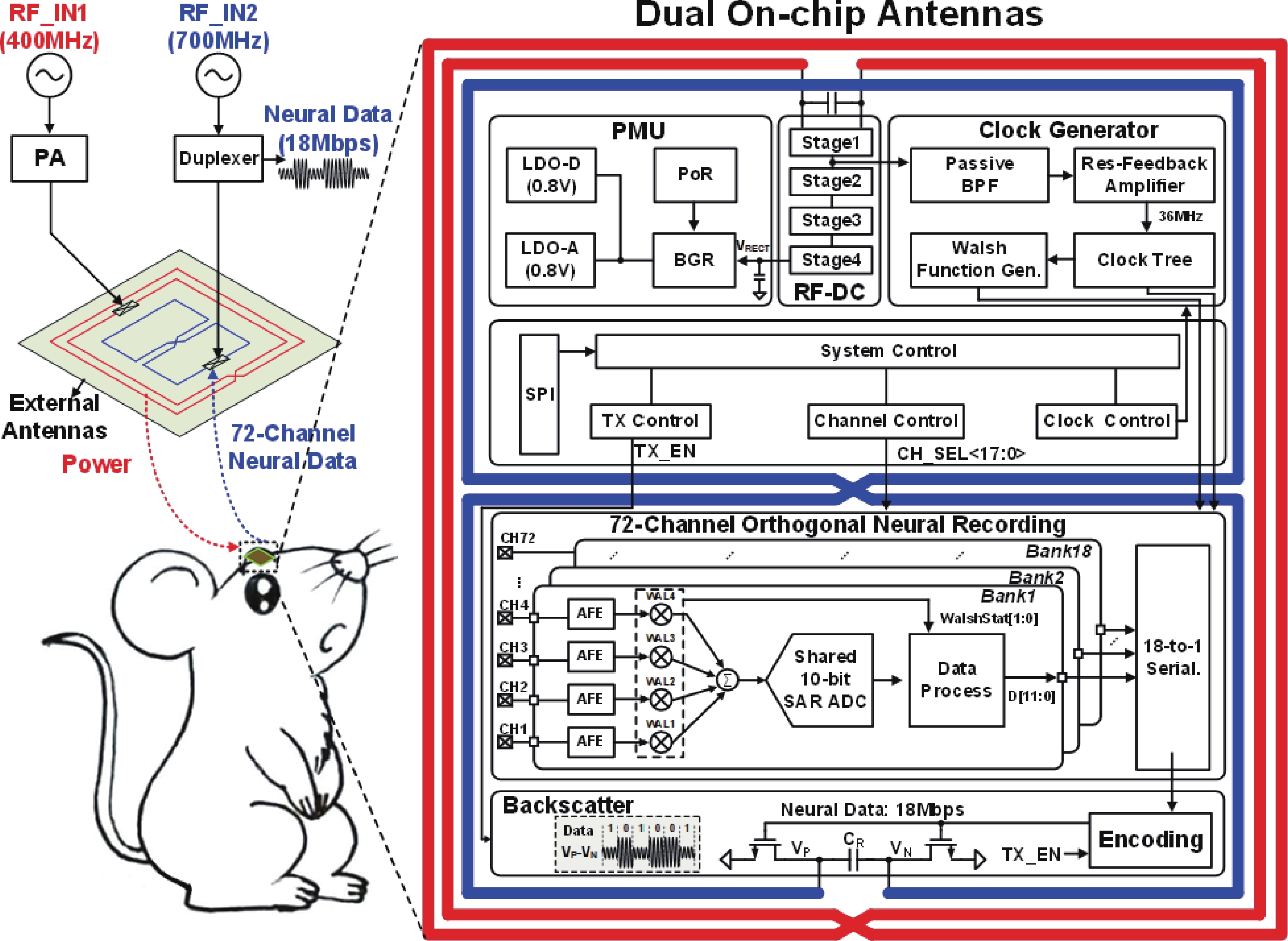
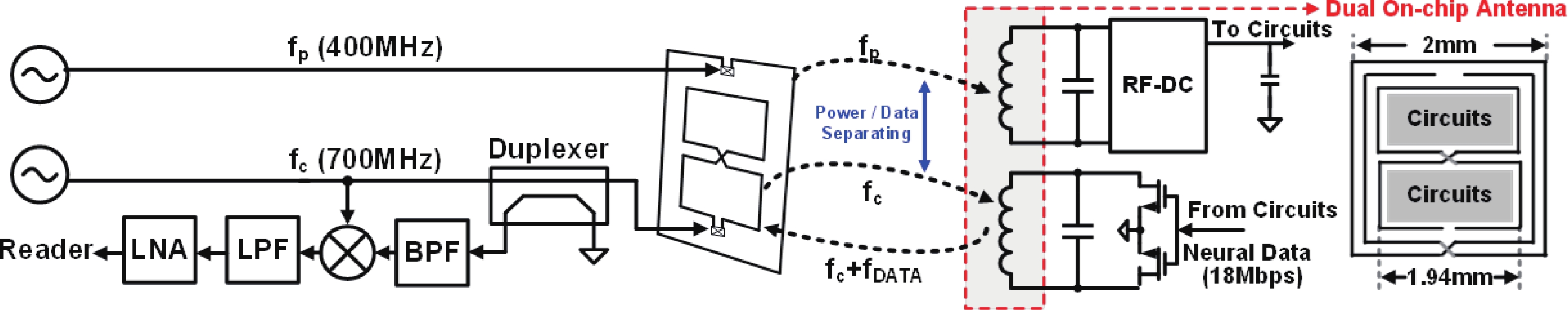
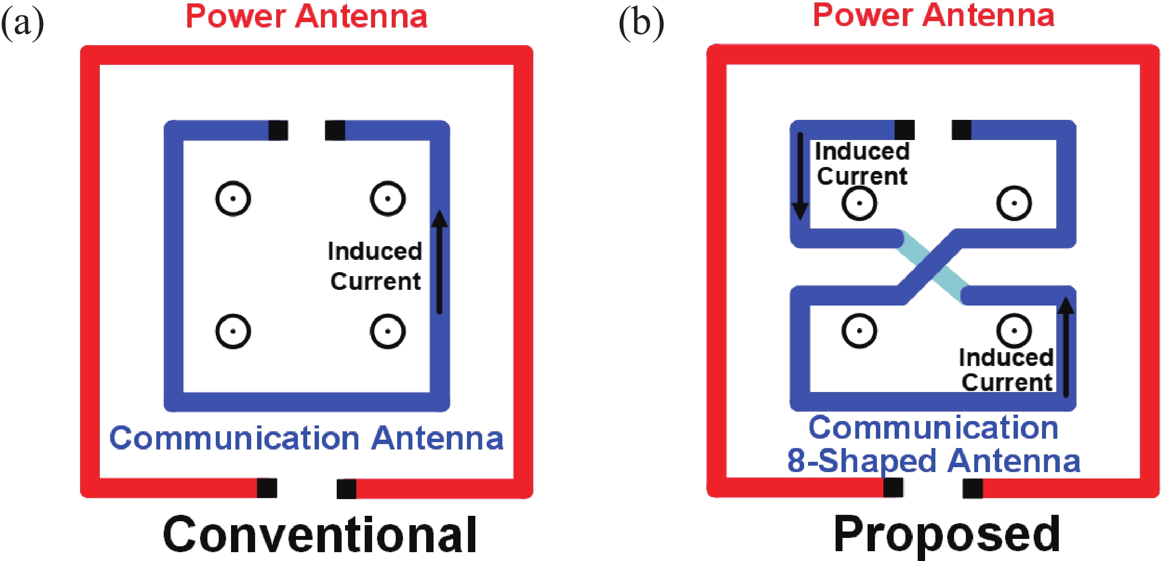
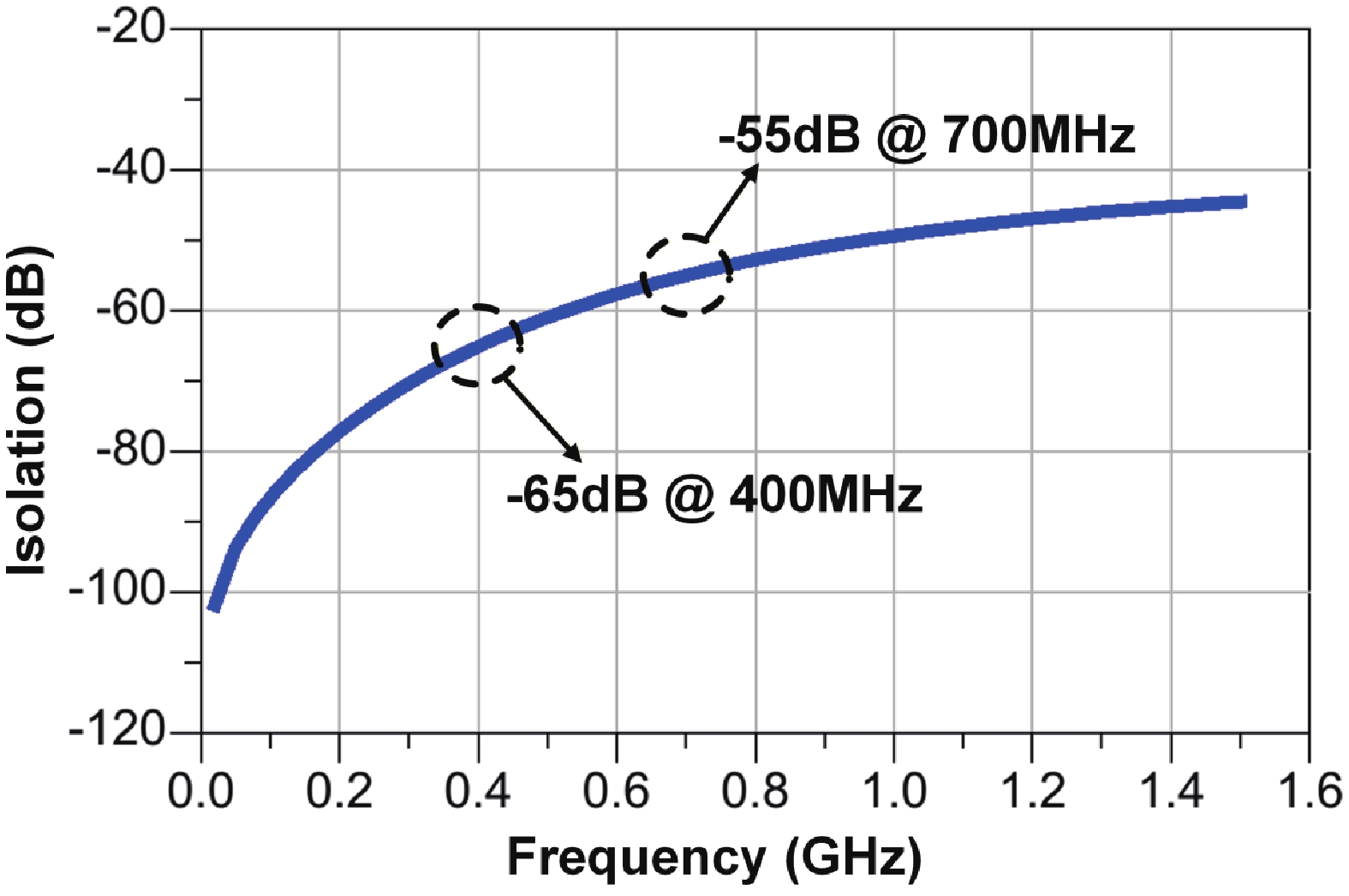
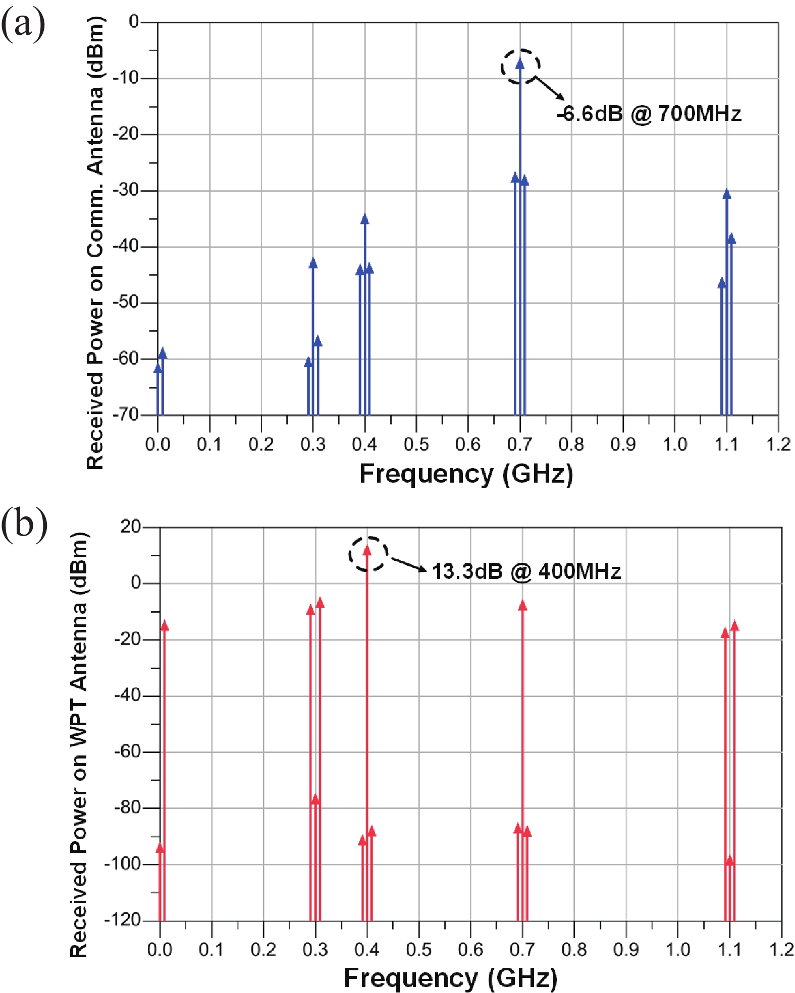
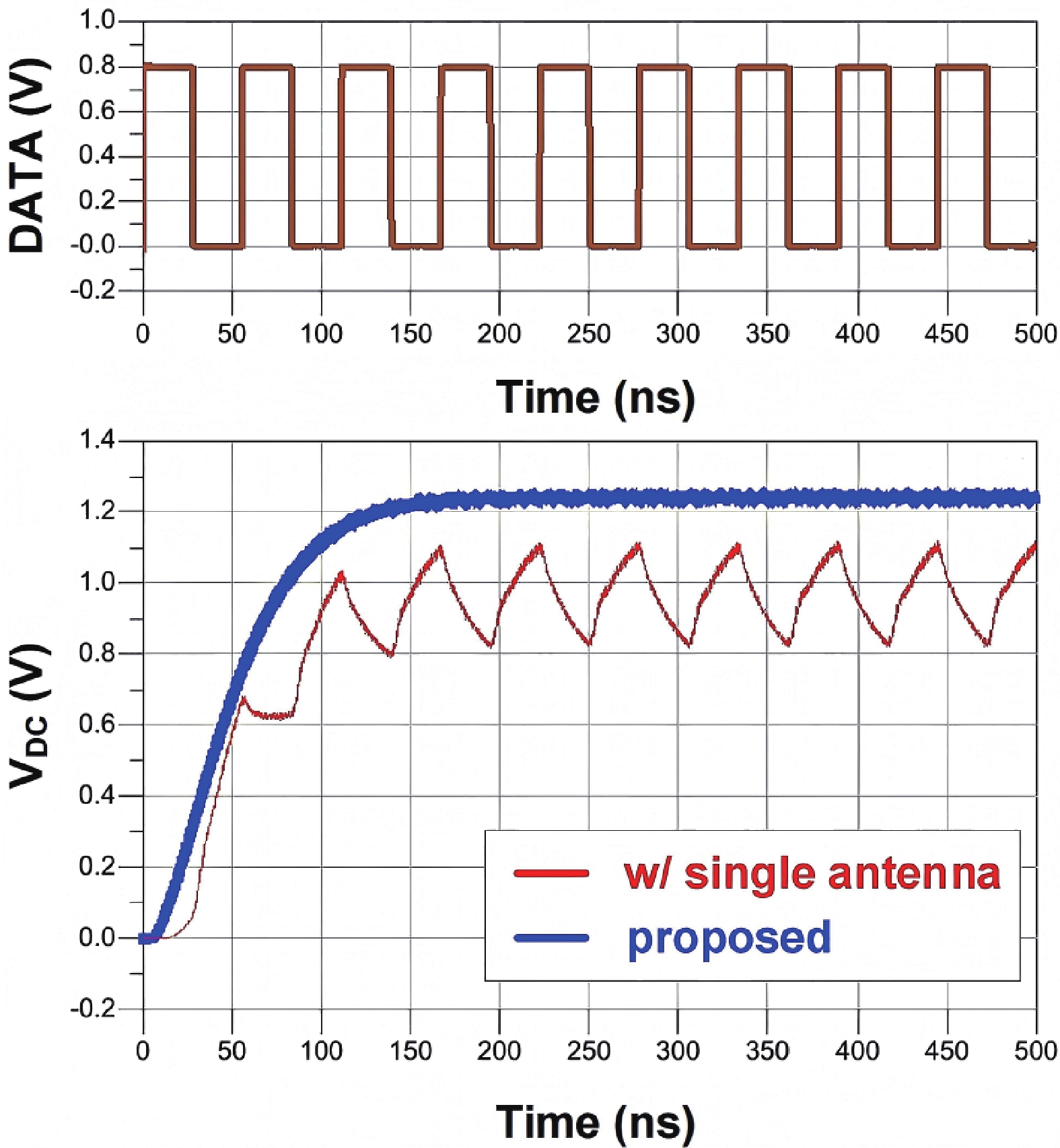
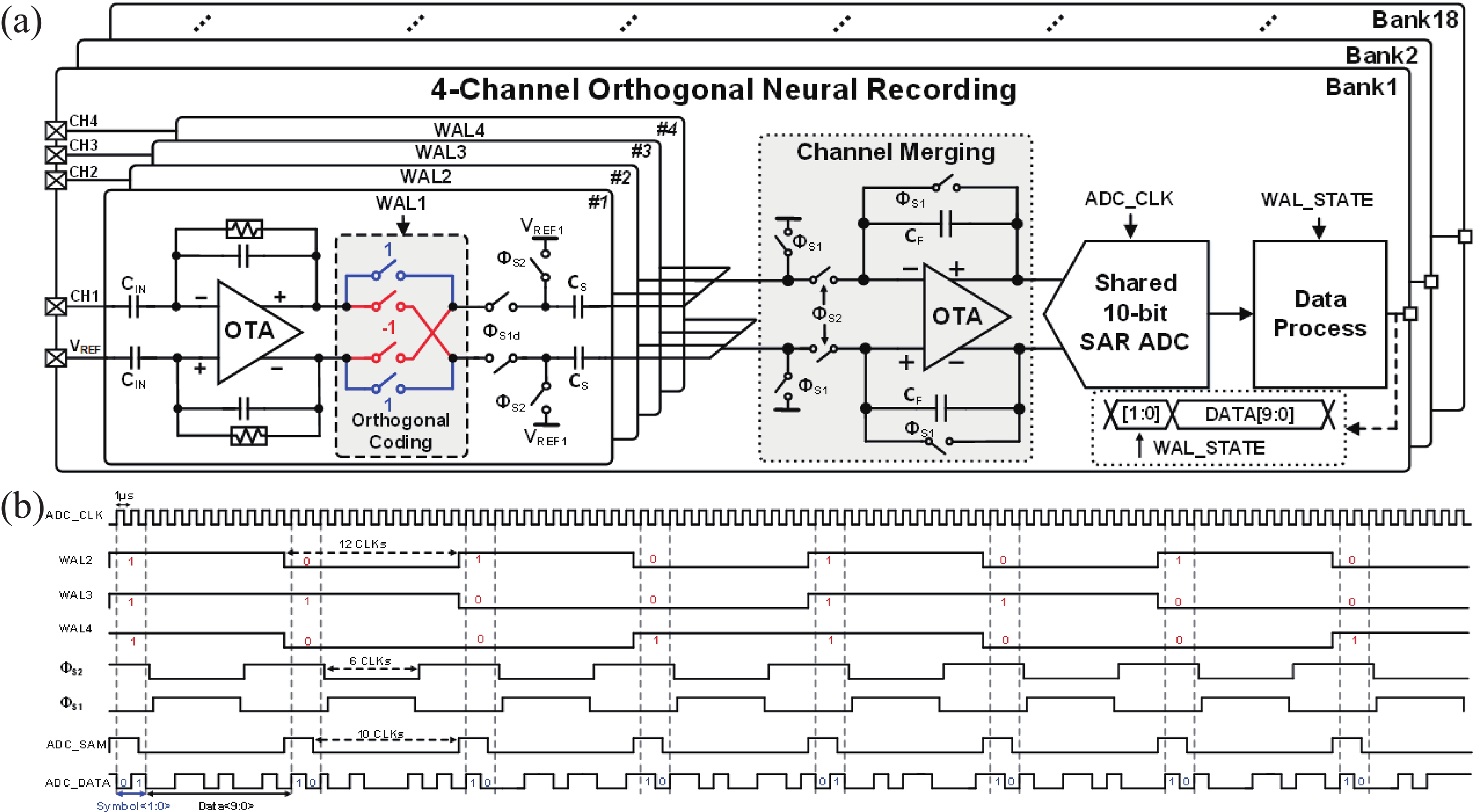
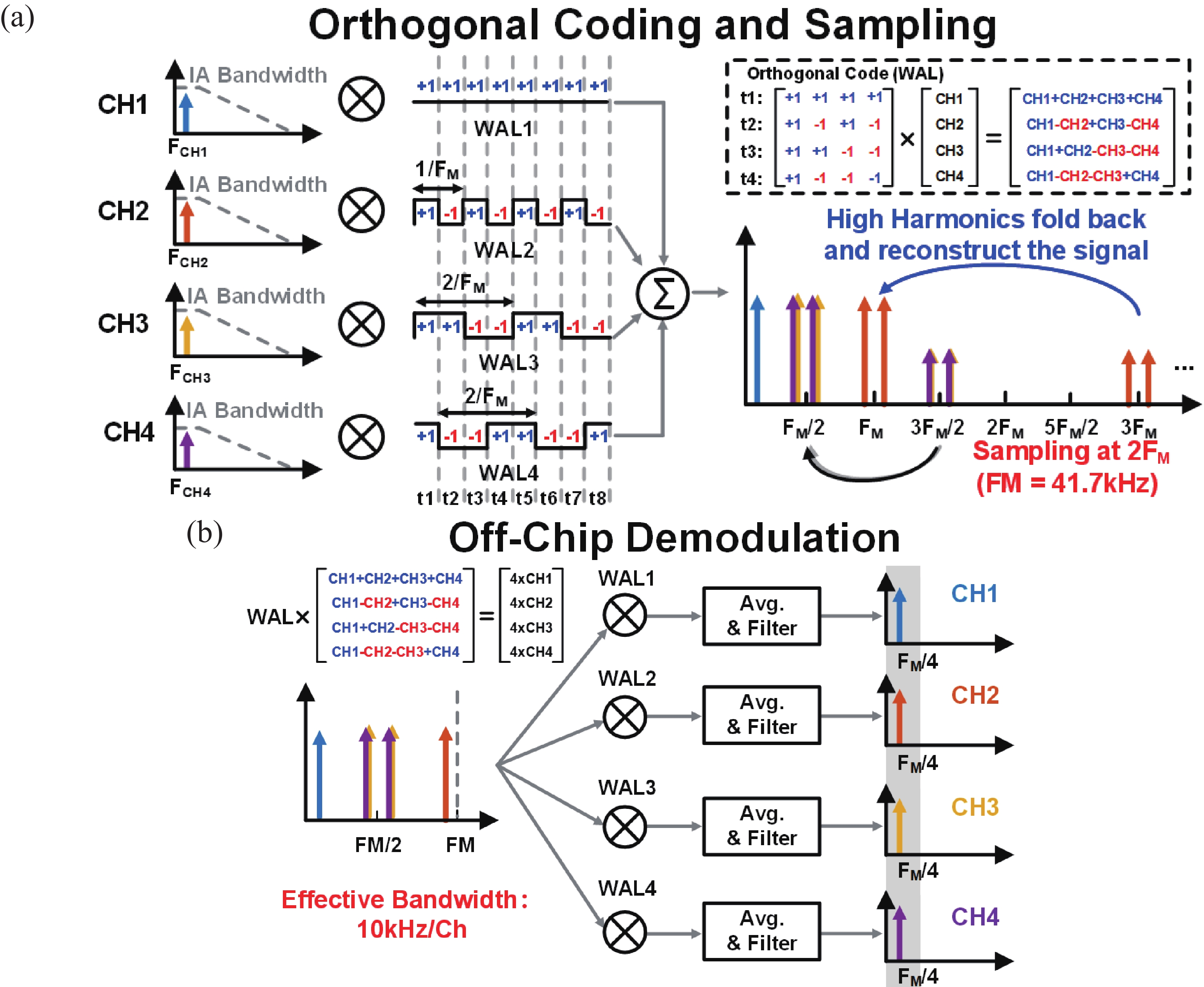
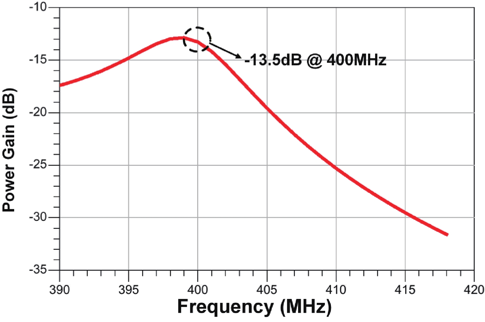
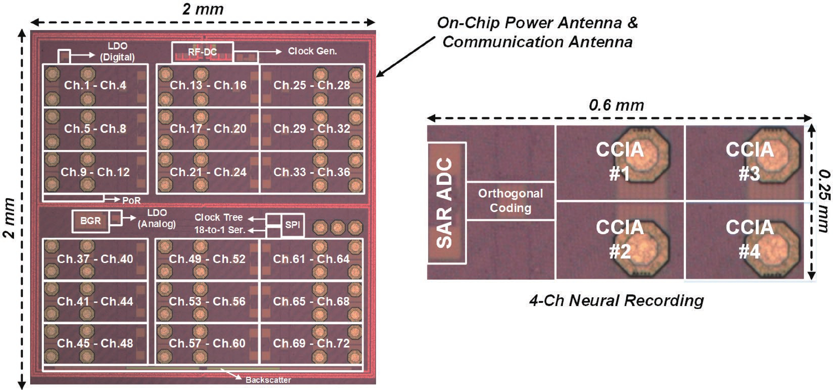
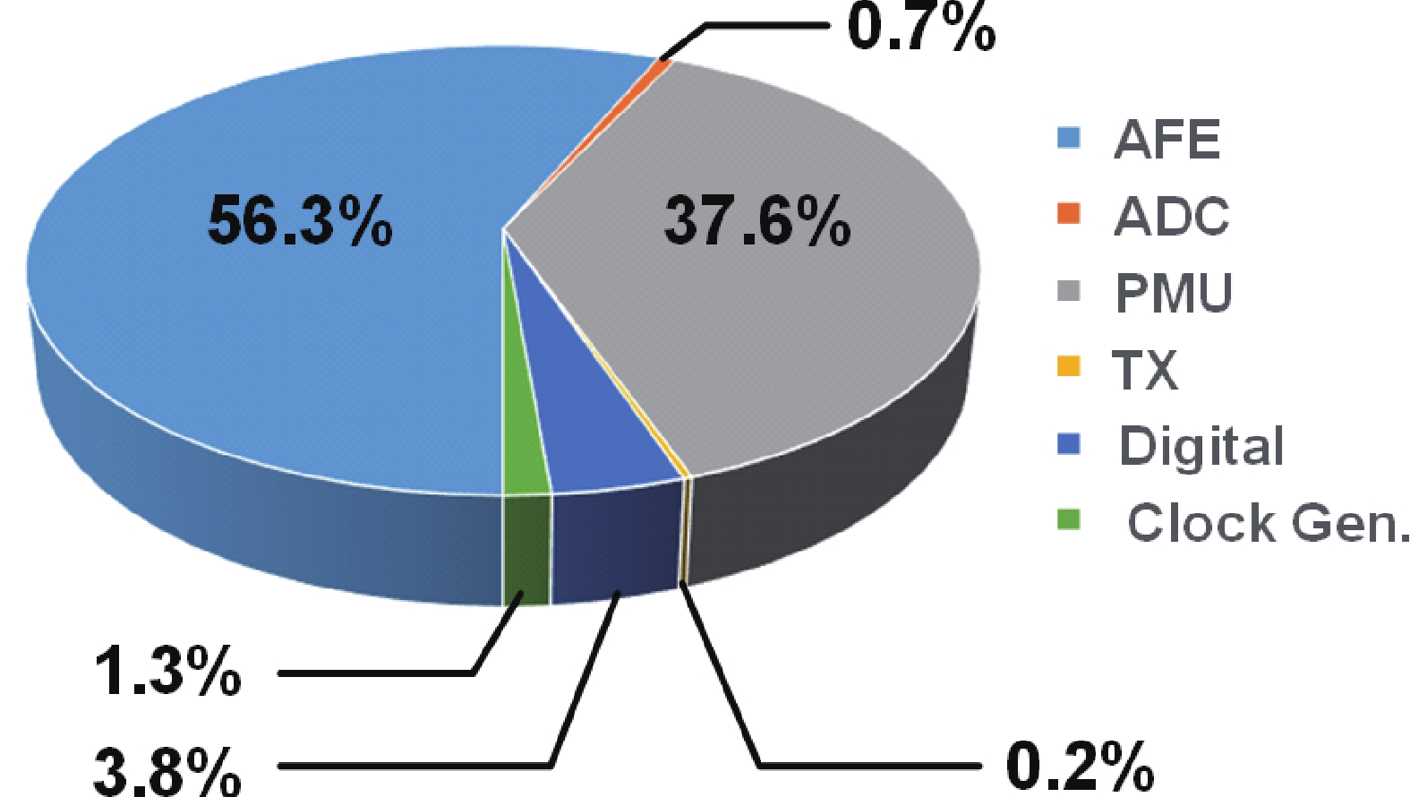
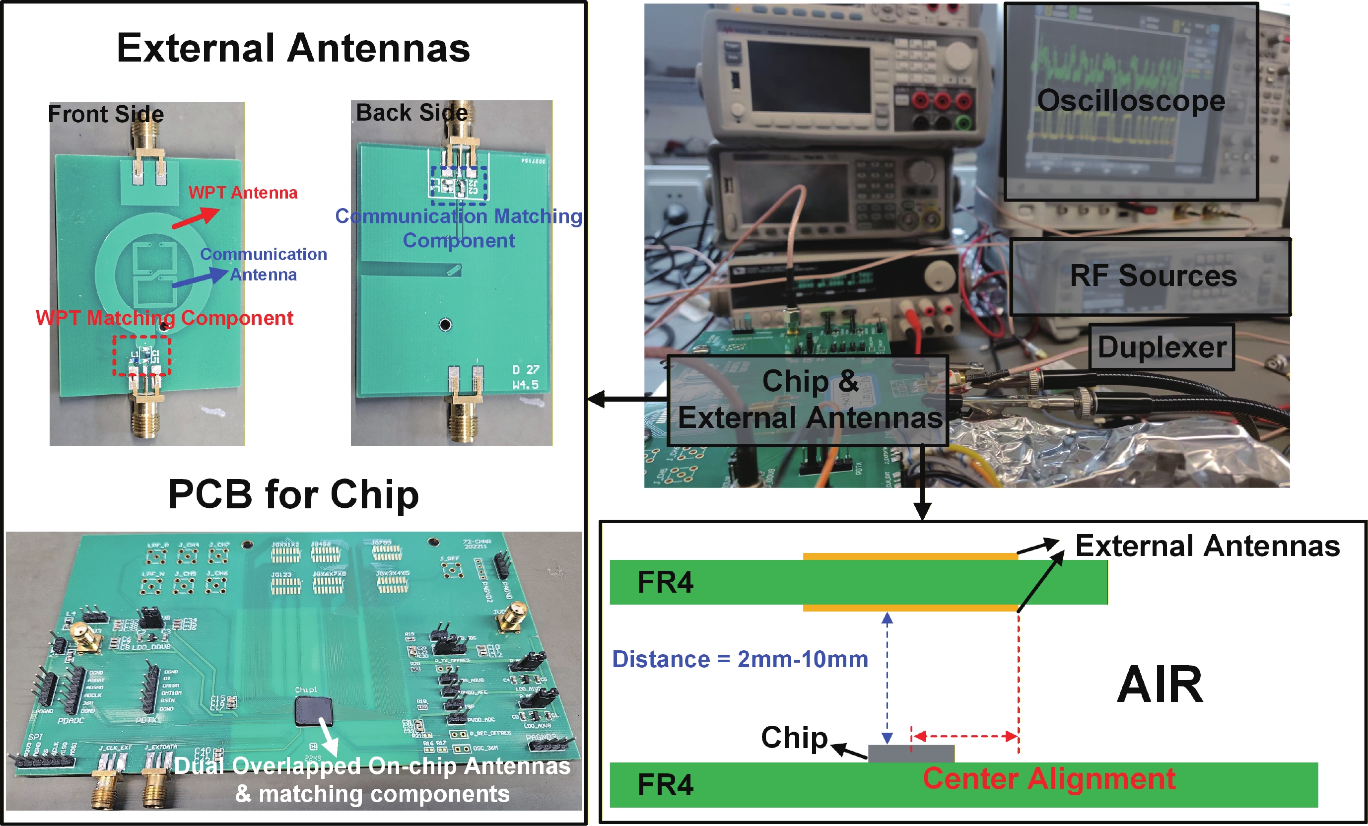
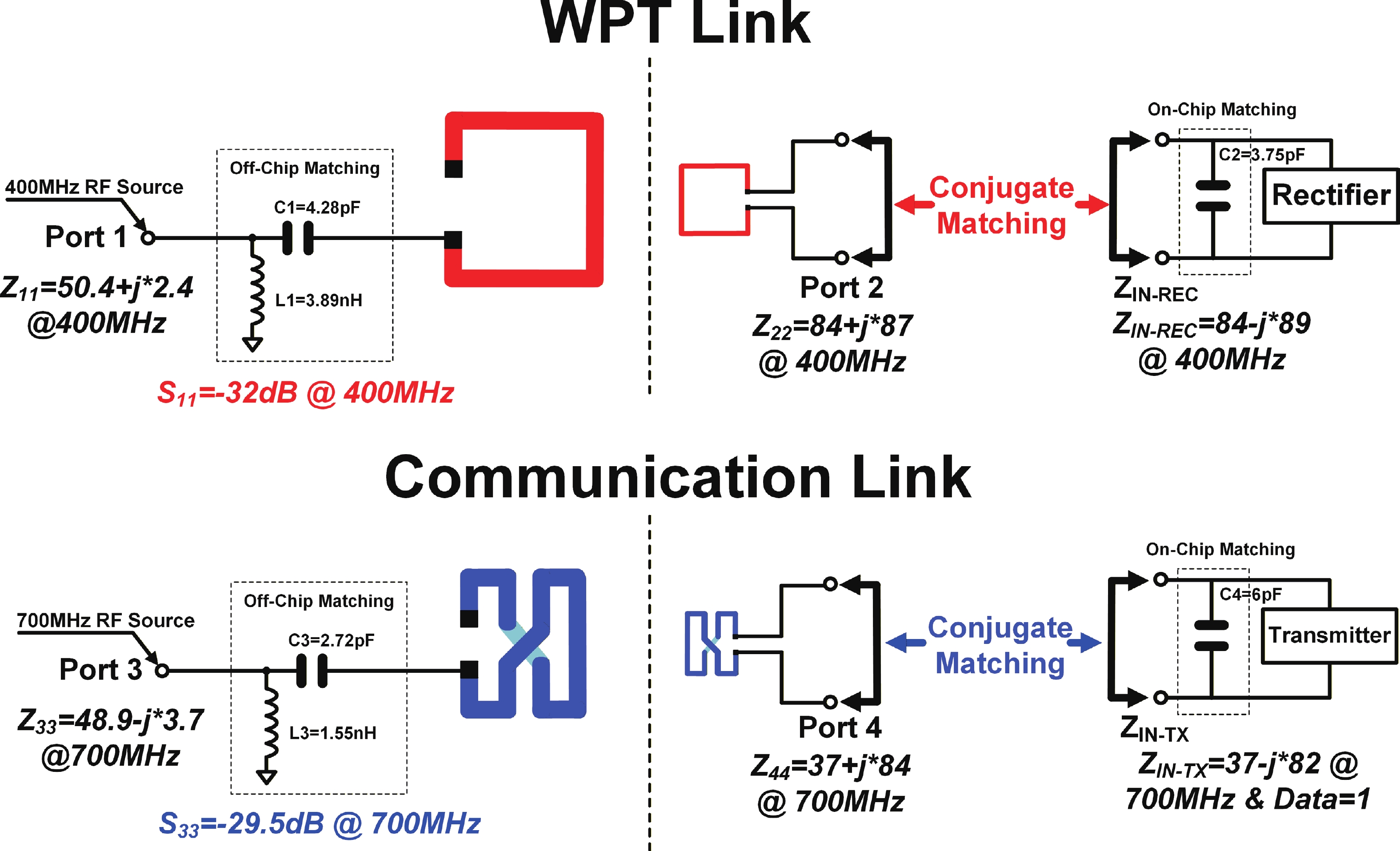
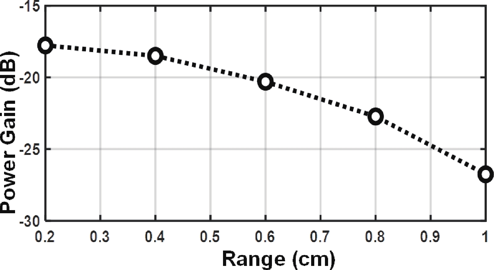
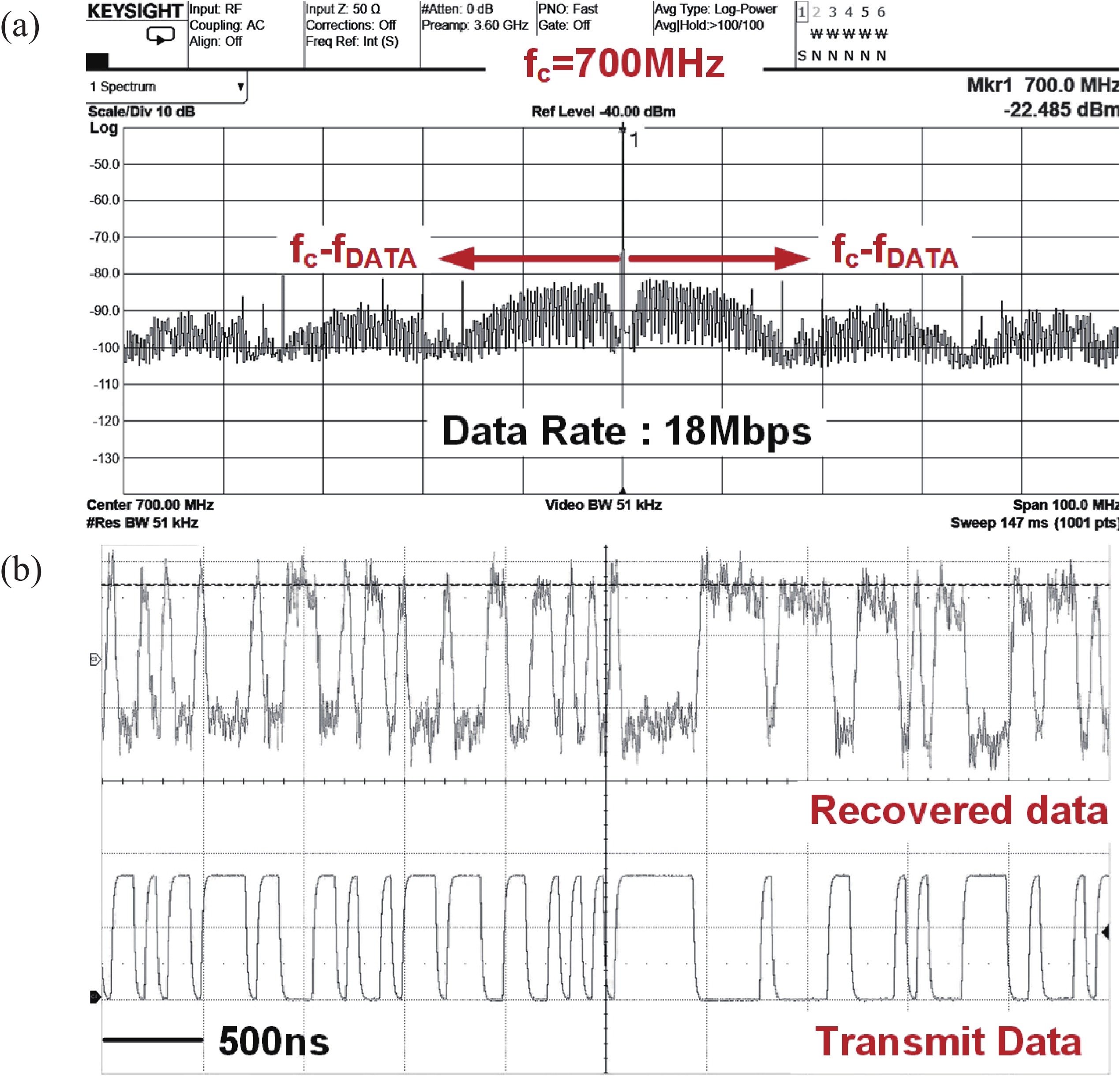
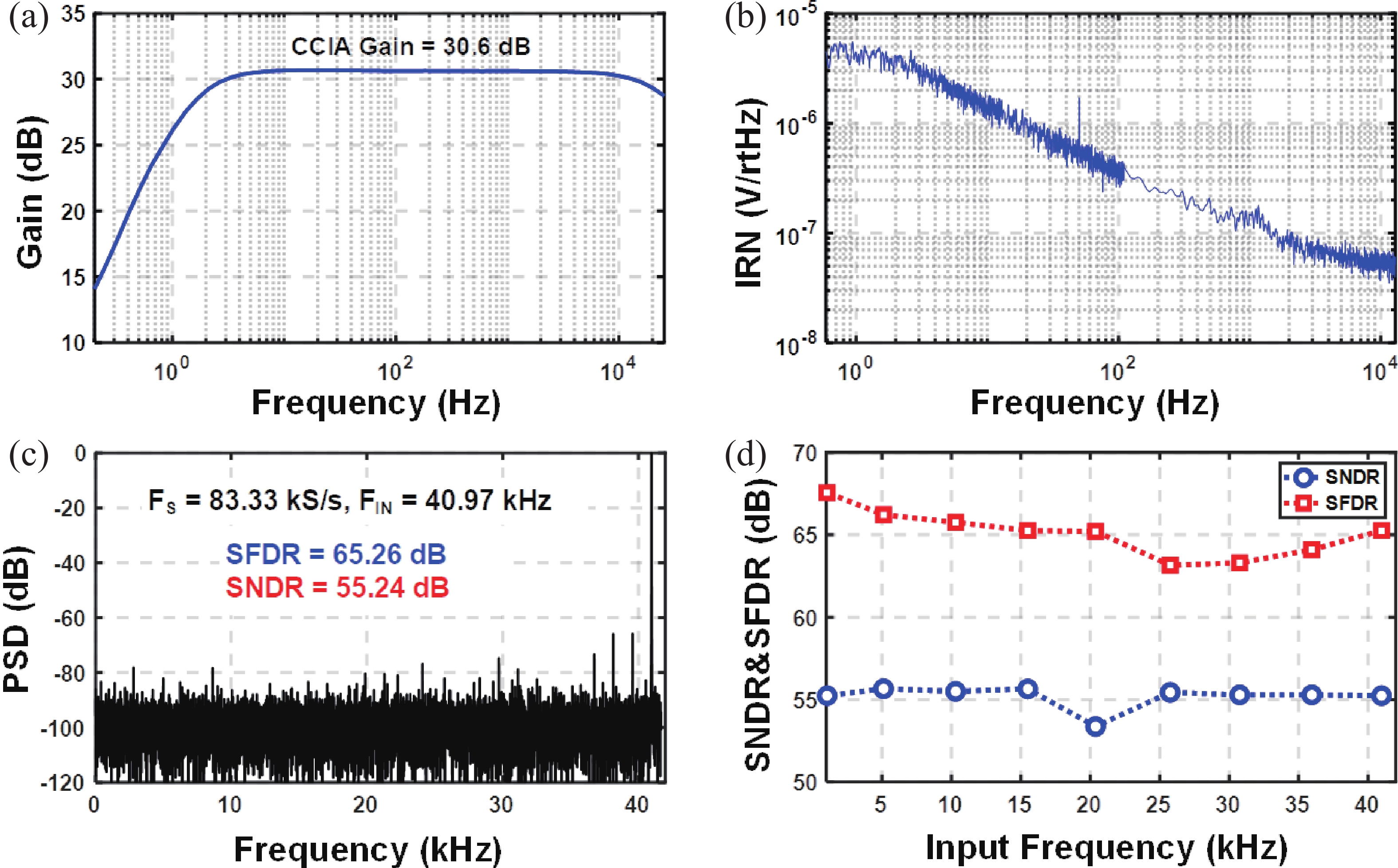
Battery-free radio systems utilizing wireless power transfer (WPT) further facilitate the miniaturization of neural implants. However, simultaneous monitoring of multiple neuronal activities is required to obtain high-fidelity neural signals. Consequently, the integration of numerous channels on a single chip and the wireless transmission of massive multi-channel data pose significant challenges for implantable battery-free neural interfaces. This work introduces dual overlapped on-chip antennas to eliminate the need for a battery in the neural implants and enable high-data-rate backscatter for transmitting the massive data acquired simultaneously from 72 channels. Additionally, an orthogonal coding and sampling technique is employed to reduce both power consumption and area per channel. Fabricated in a 65 nm CMOS process, the proposed chip integrates 72 neural recording channels within a 2 mm × 2 mm area and achieves a backscatter data rate of 18 Mbps.
J. Semicond.
2026, 47(6): 062202 doi: 10.1088/1674-4926/25120023
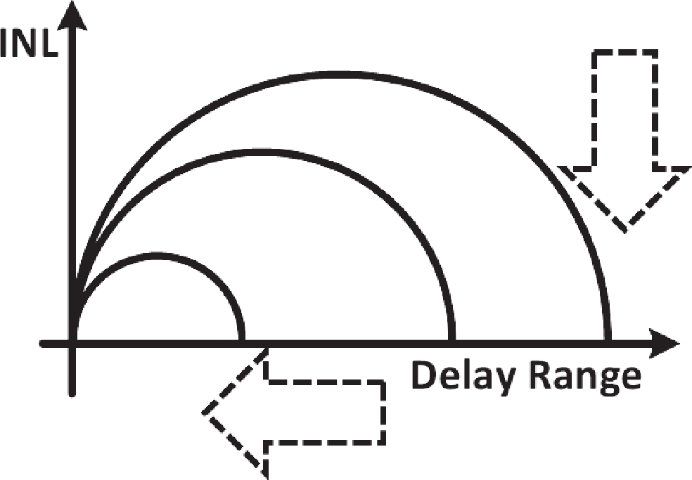
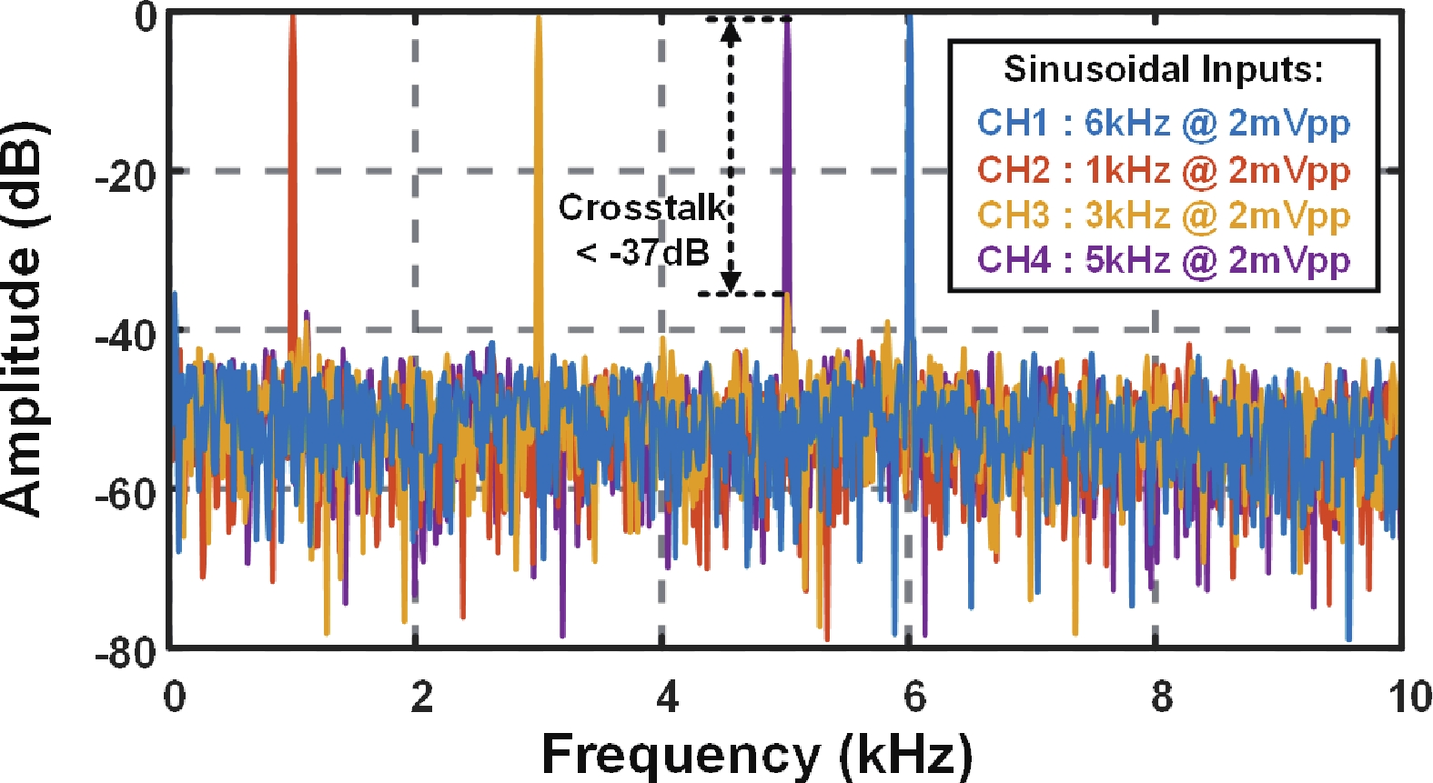
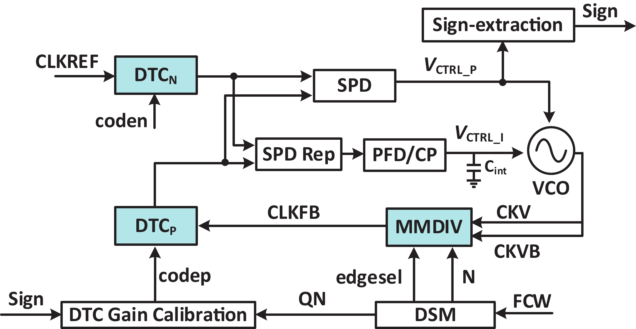
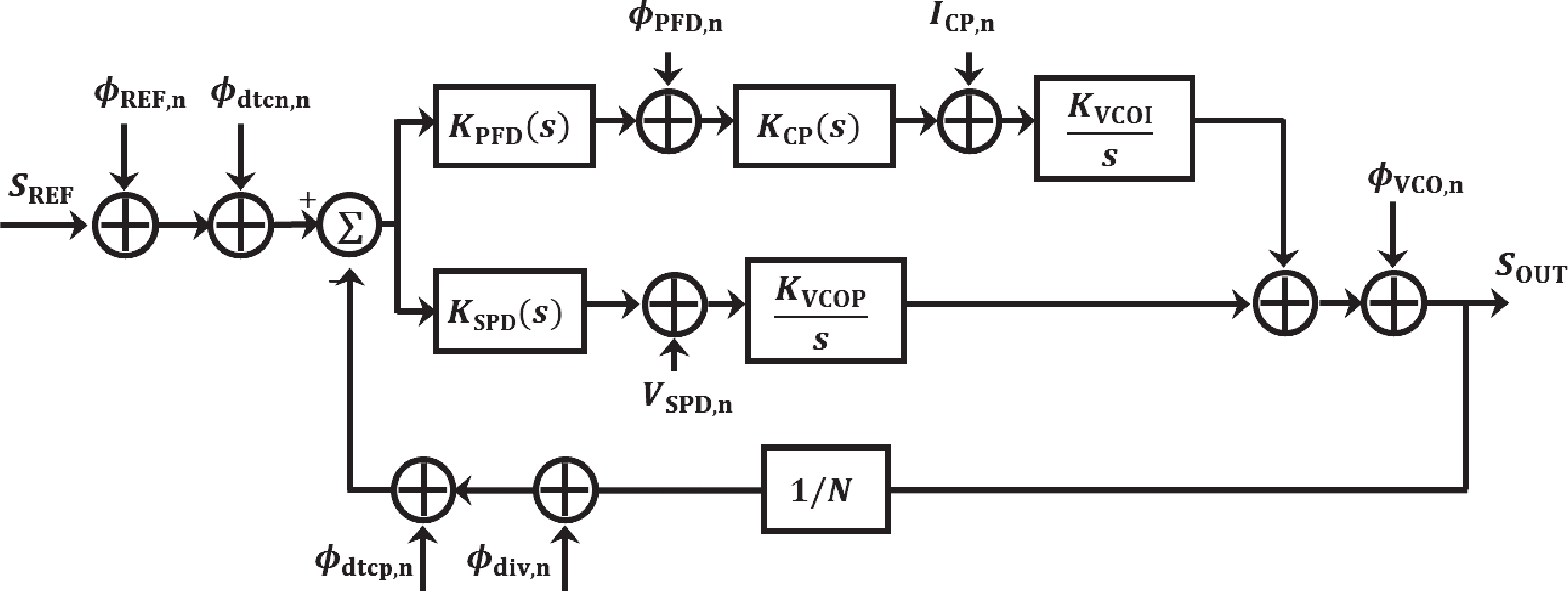
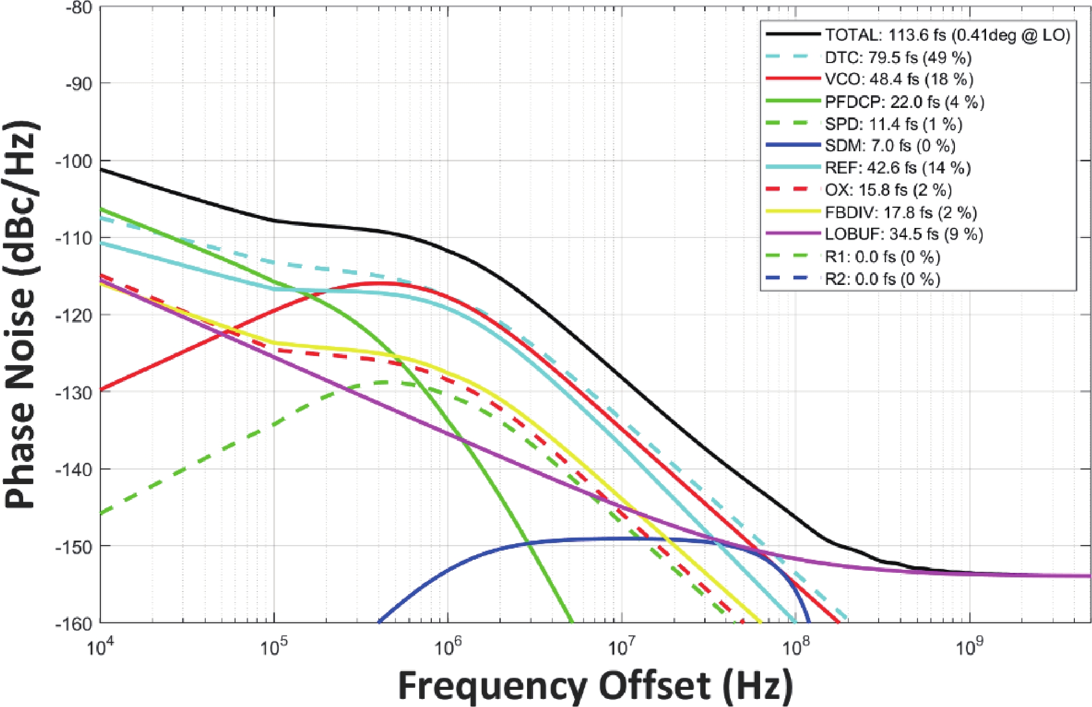
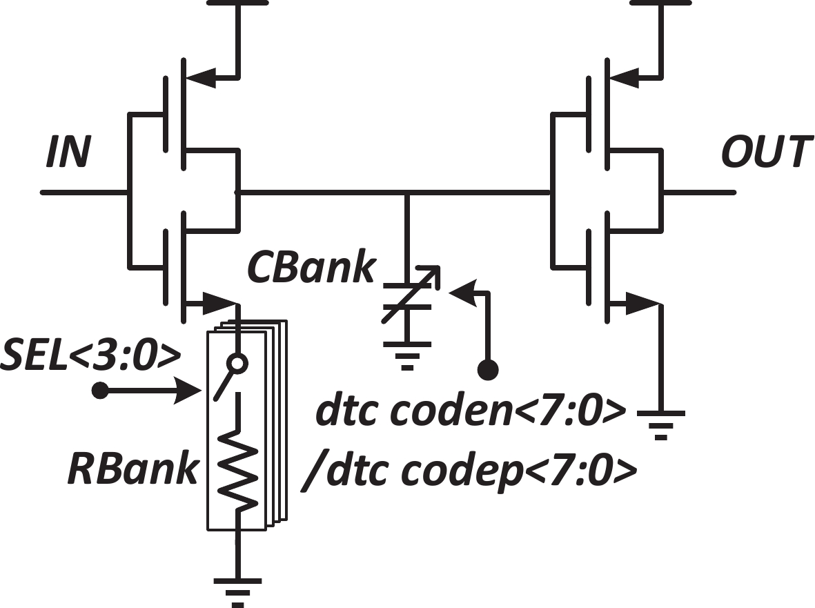
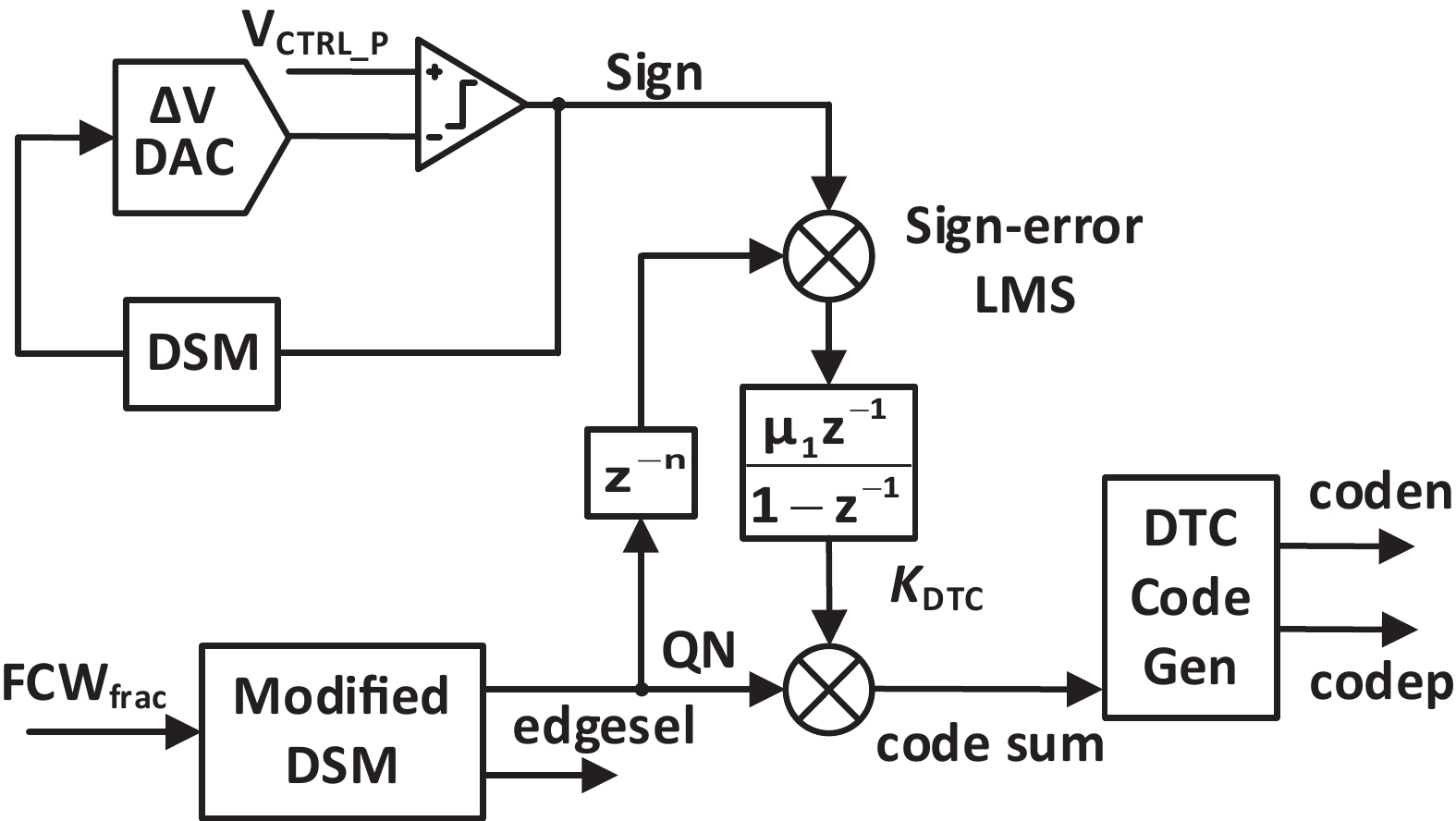
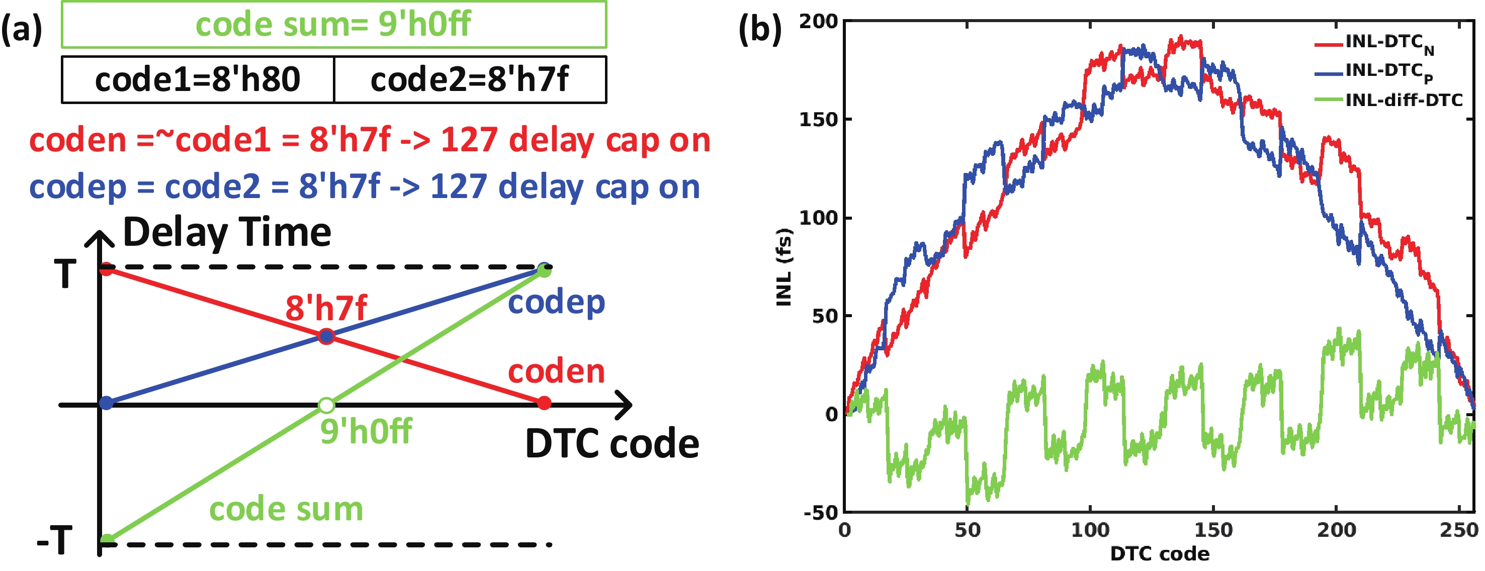
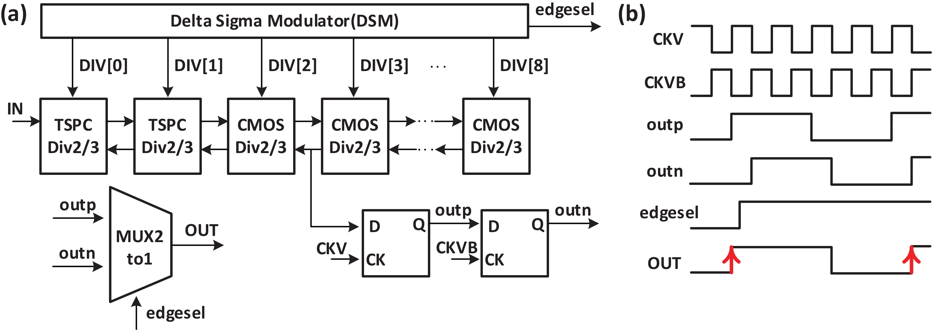
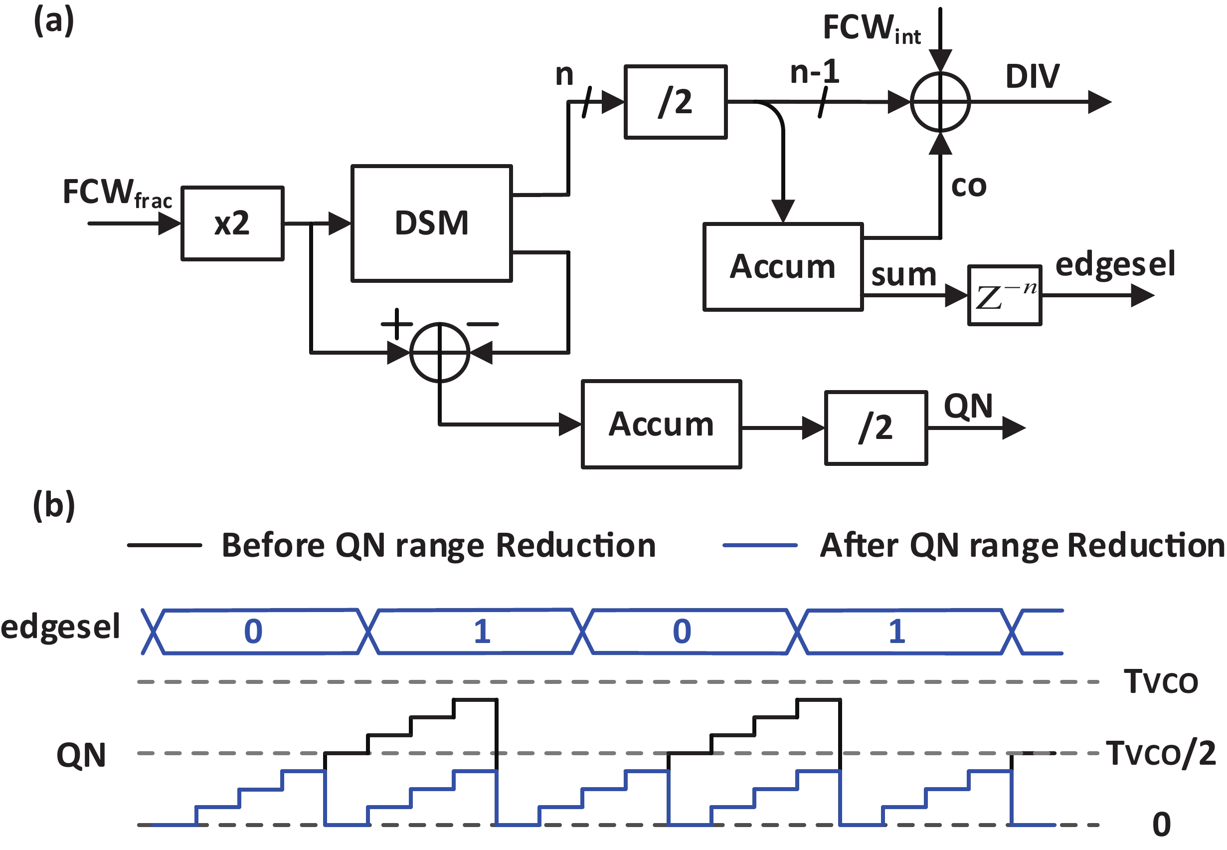
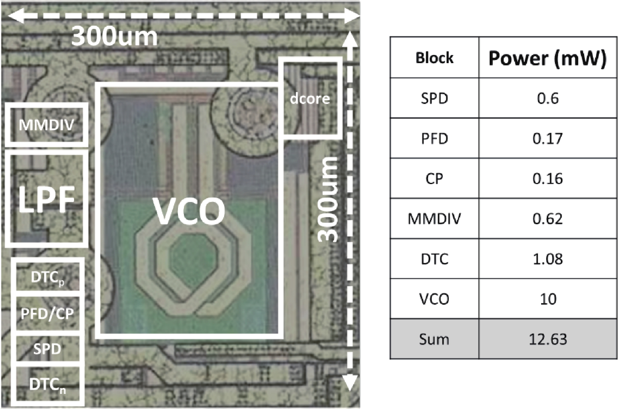
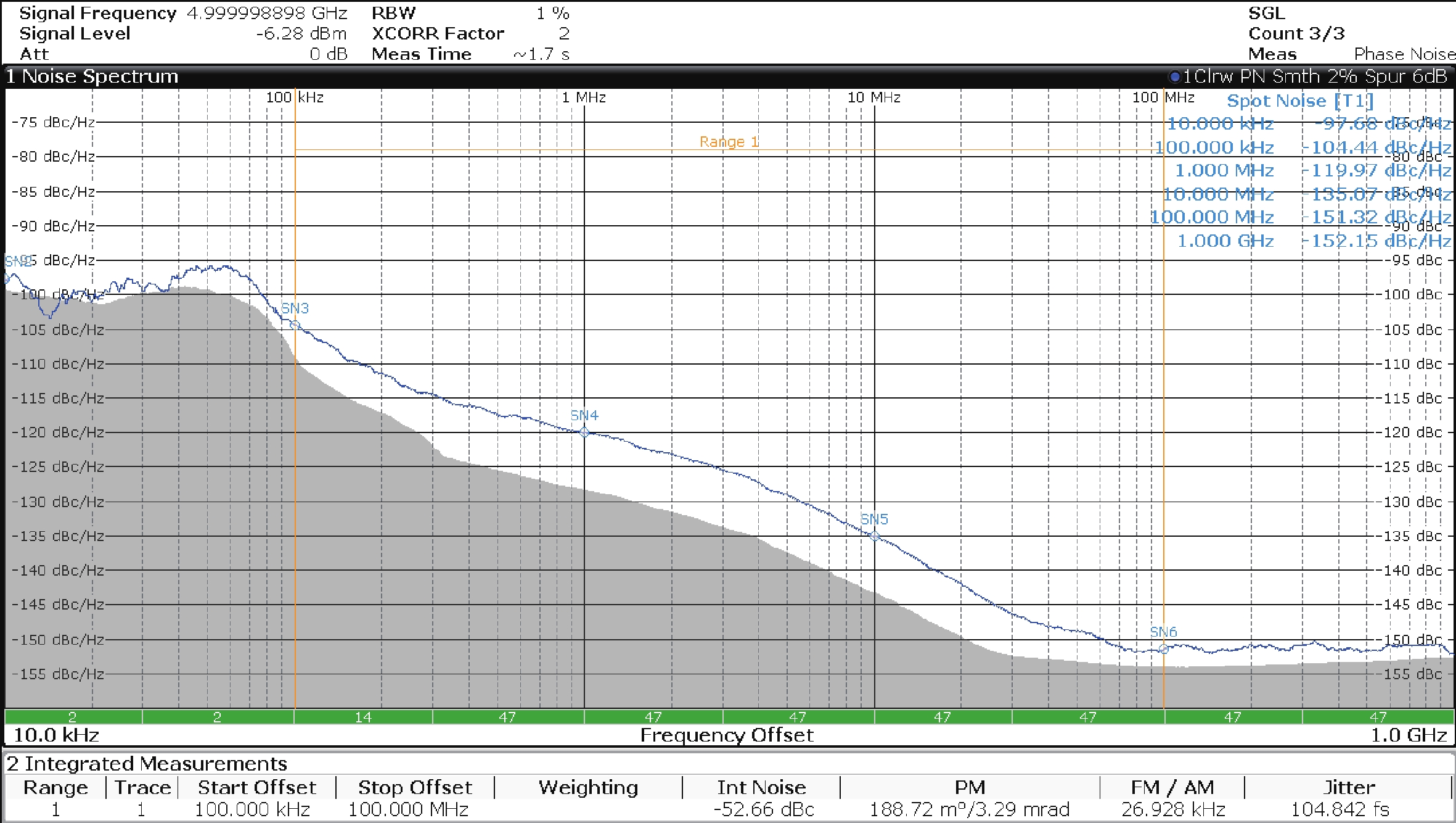
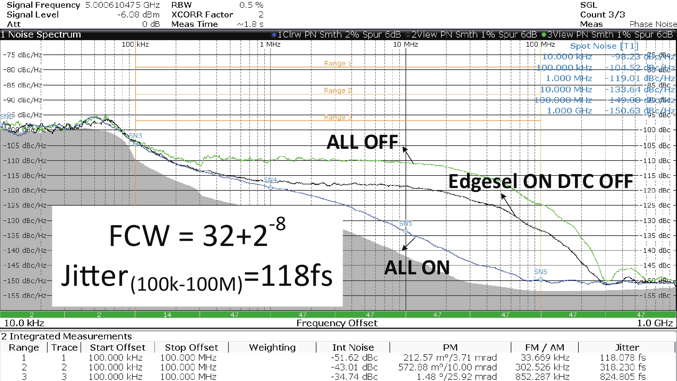
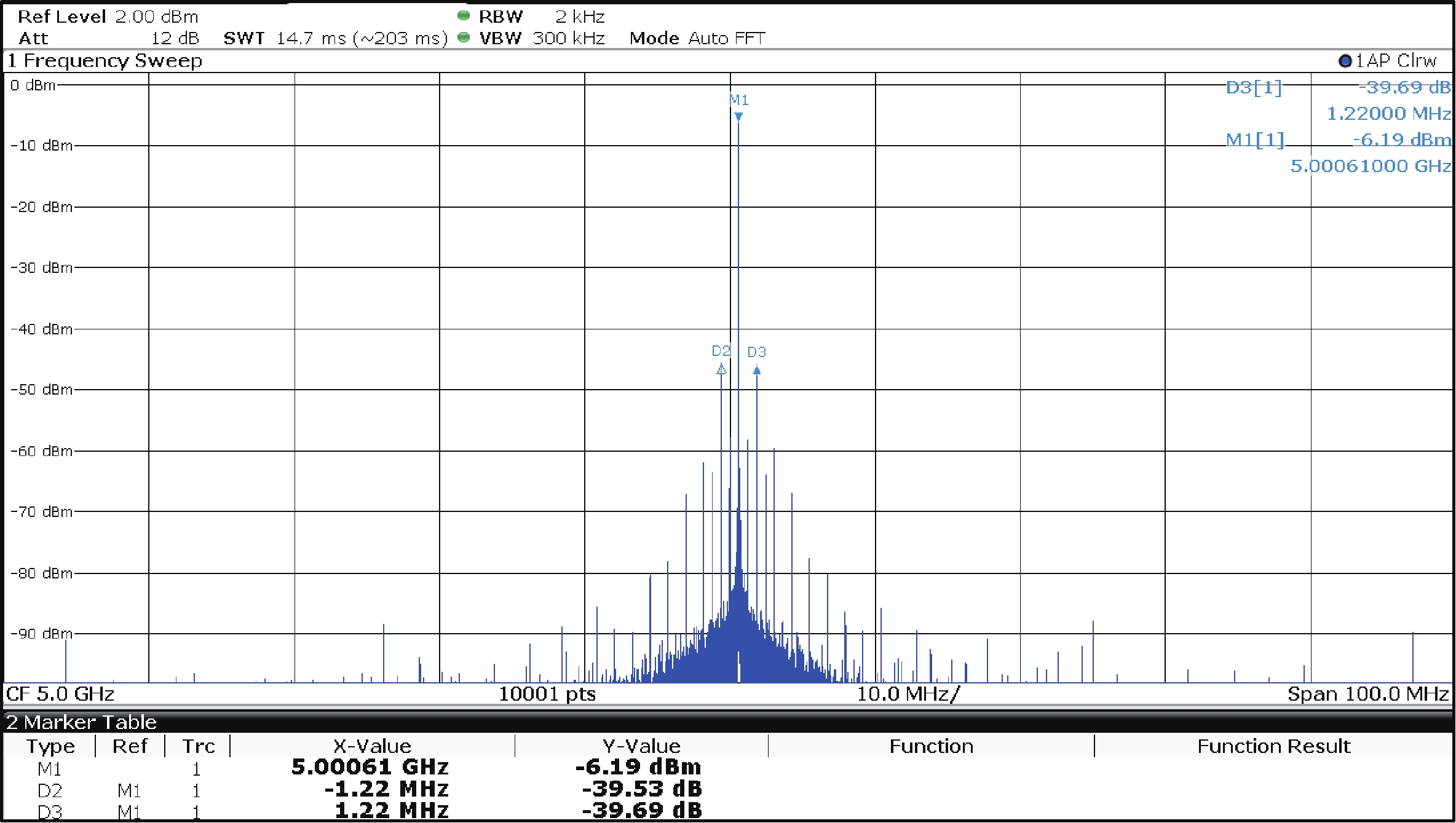
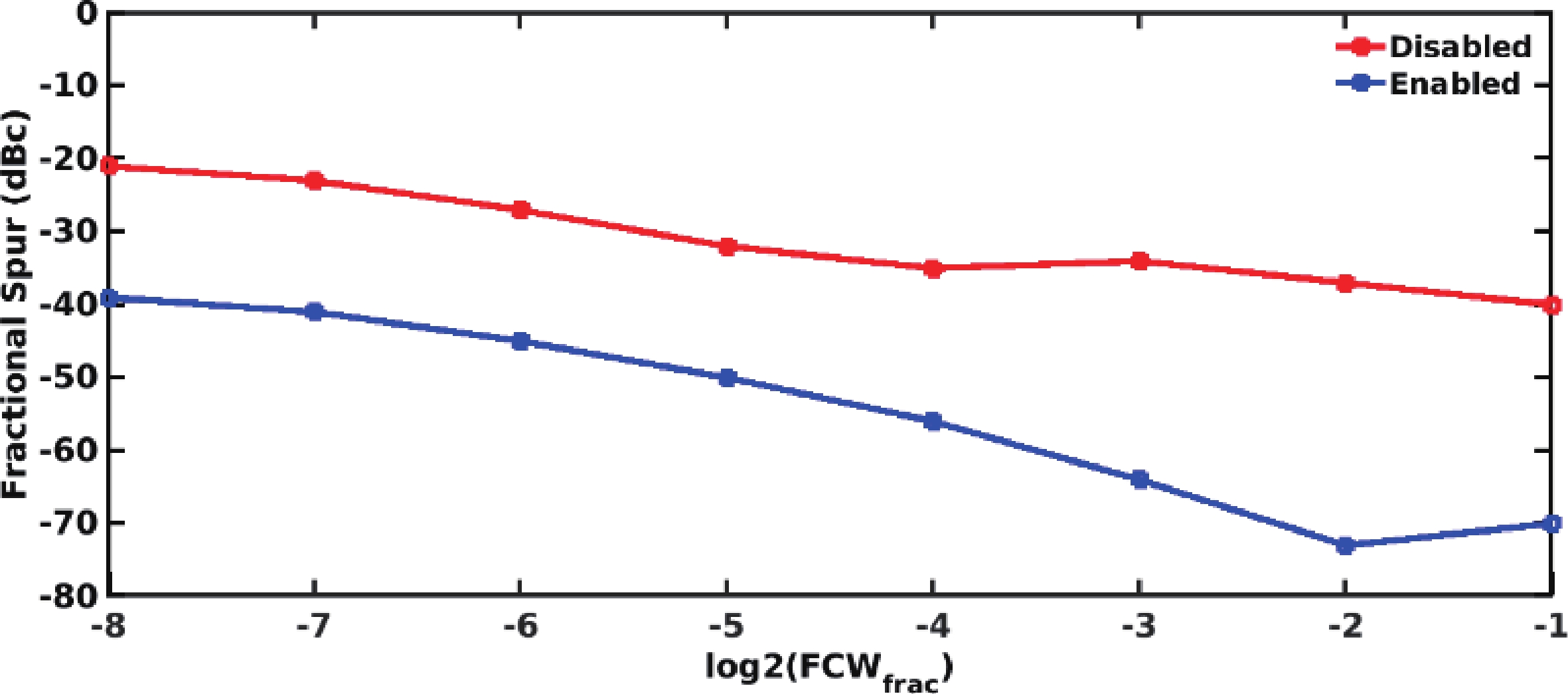
In fractional-N phase-locked loops, minimizing the integral nonlinearity (INL) of the digital-to-time converter (DTC) is crucial since it directly limits PLL performance. Considering the trade-off between DTC delay range and linearity, this paper presents a fractional-N dual-path SPD/PFD PLL (DP-SPFDPLL) with a complementary DTC pair. Controlled by the complementary control words, two DTCs are introduced before the two inputs of the phase detector for DTC range reduction and INL cancellation. The required DTC range is further halved by using differential VCO outputs to retime the frequency divider output. The overall design collectively achieves a 4× reduction in DTC range requirement. Fabricated in 7 nm FinFET, the DP-SPFDPLL achieves 118 fs RMS jitter and −247.5 dB figure-of-merit.

J. Semicond.
2026, 47(6): 062203 doi: 10.1088/1674-4926/25120024
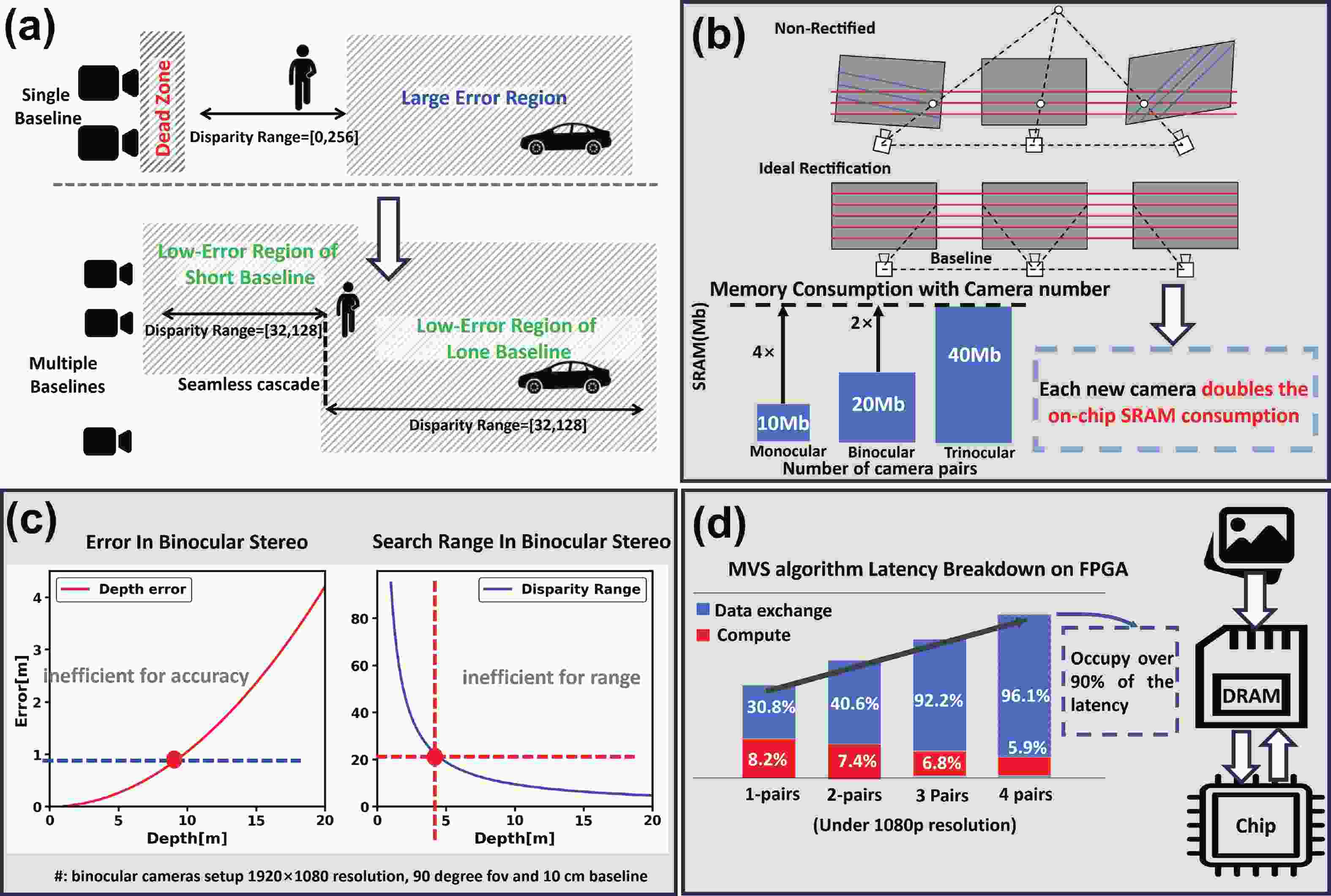
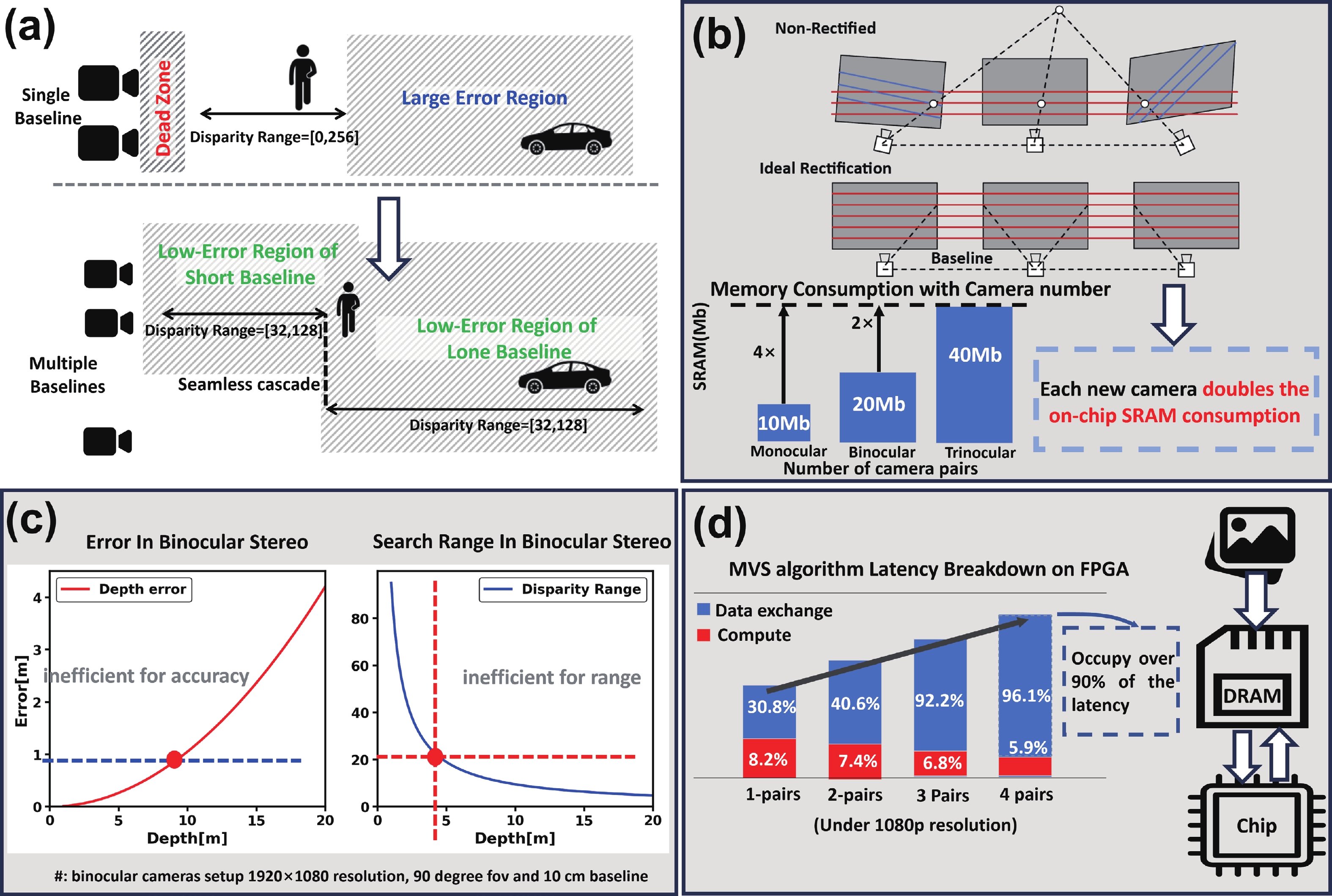
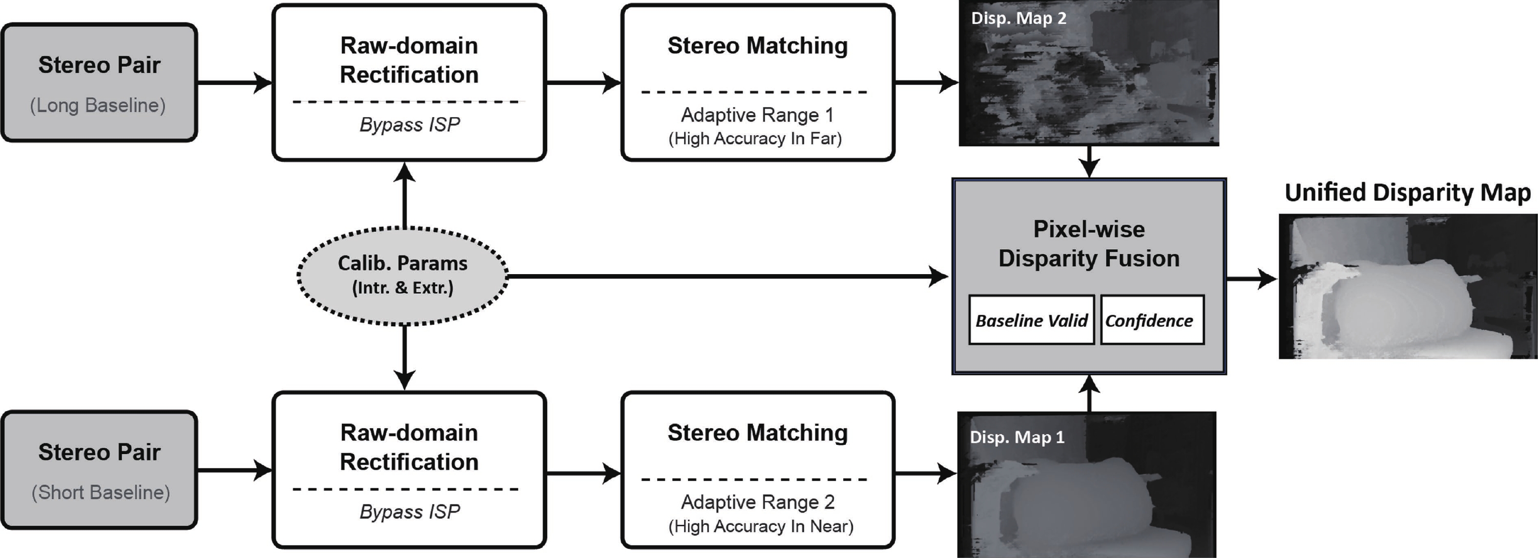
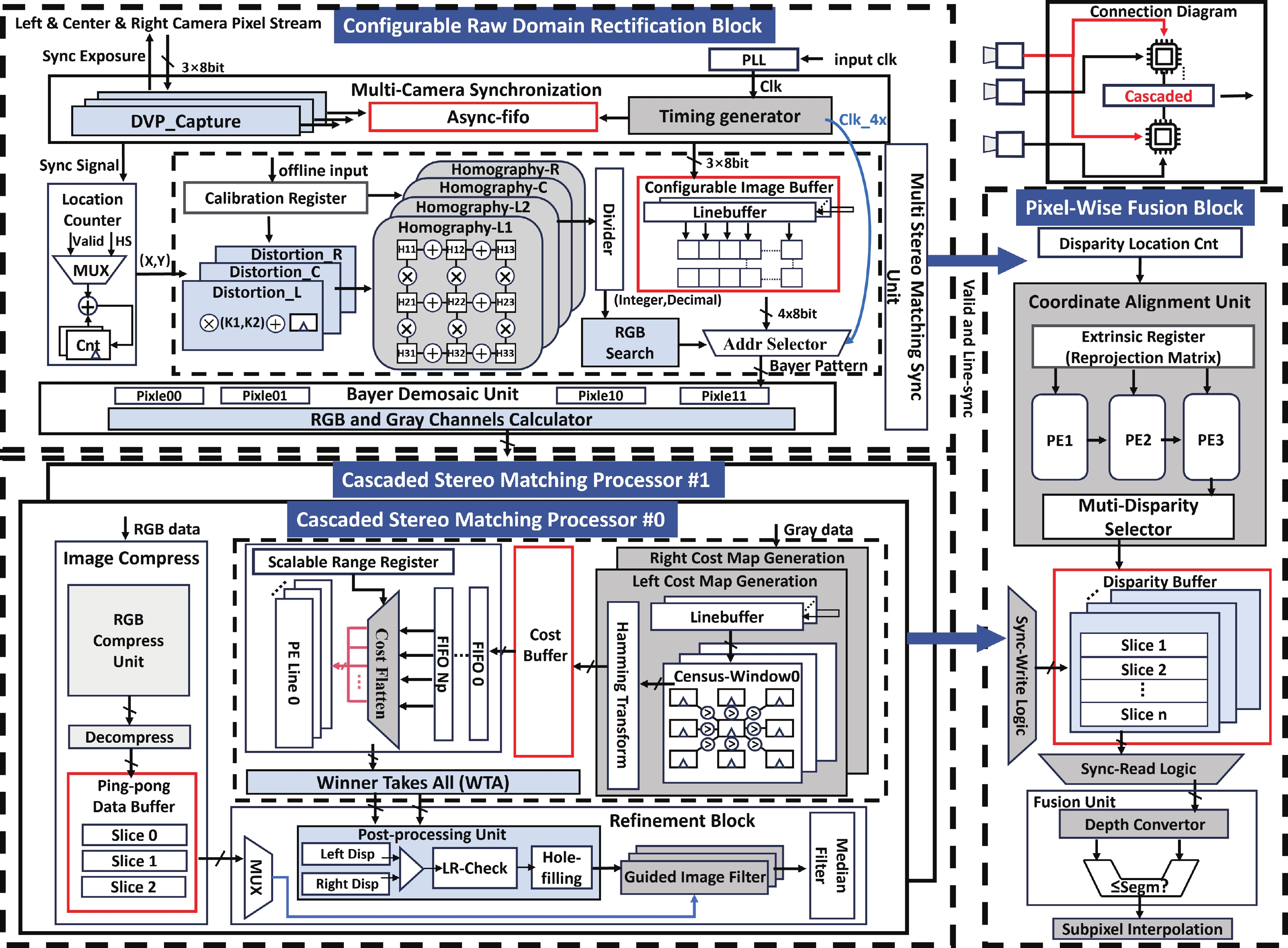
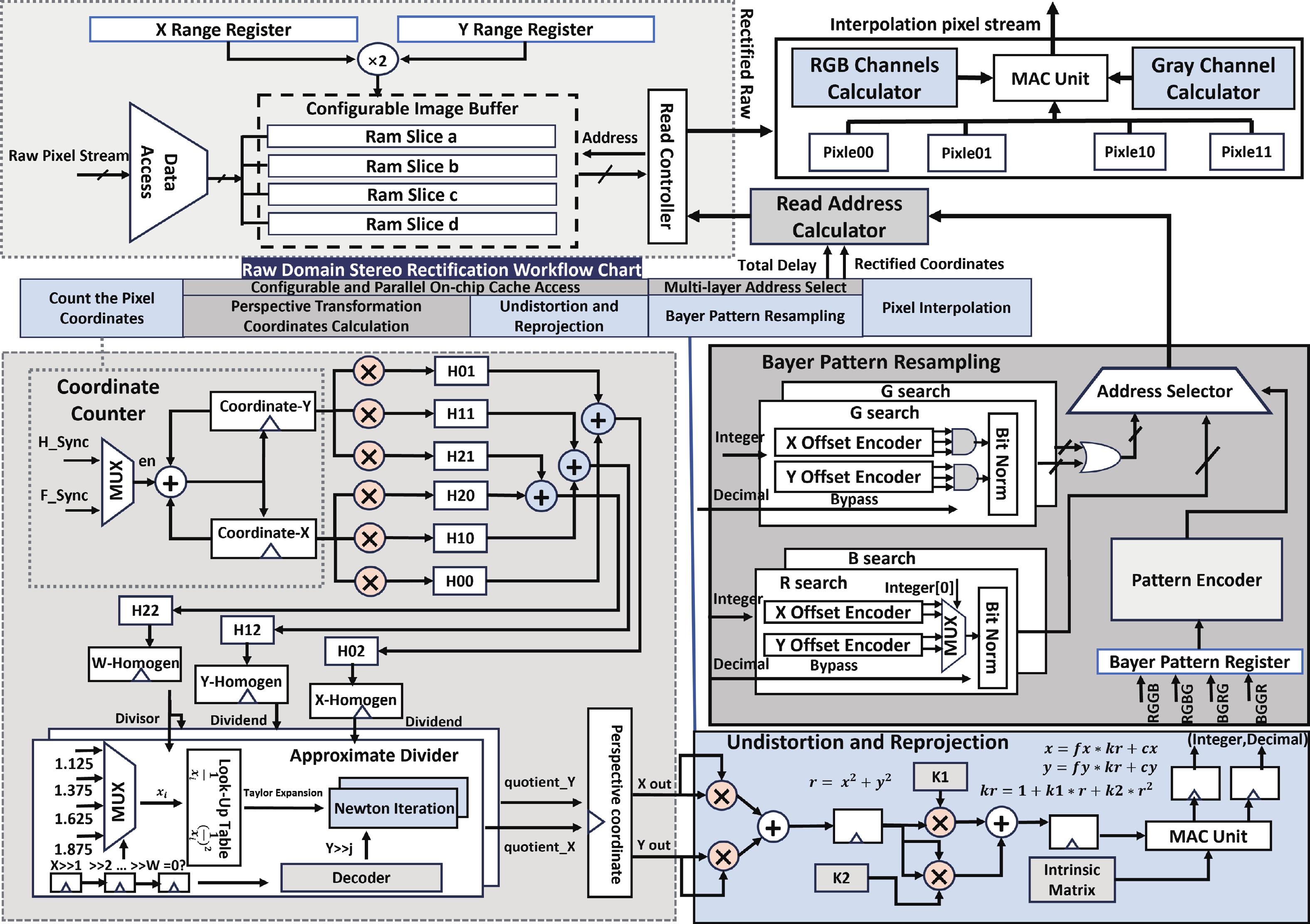
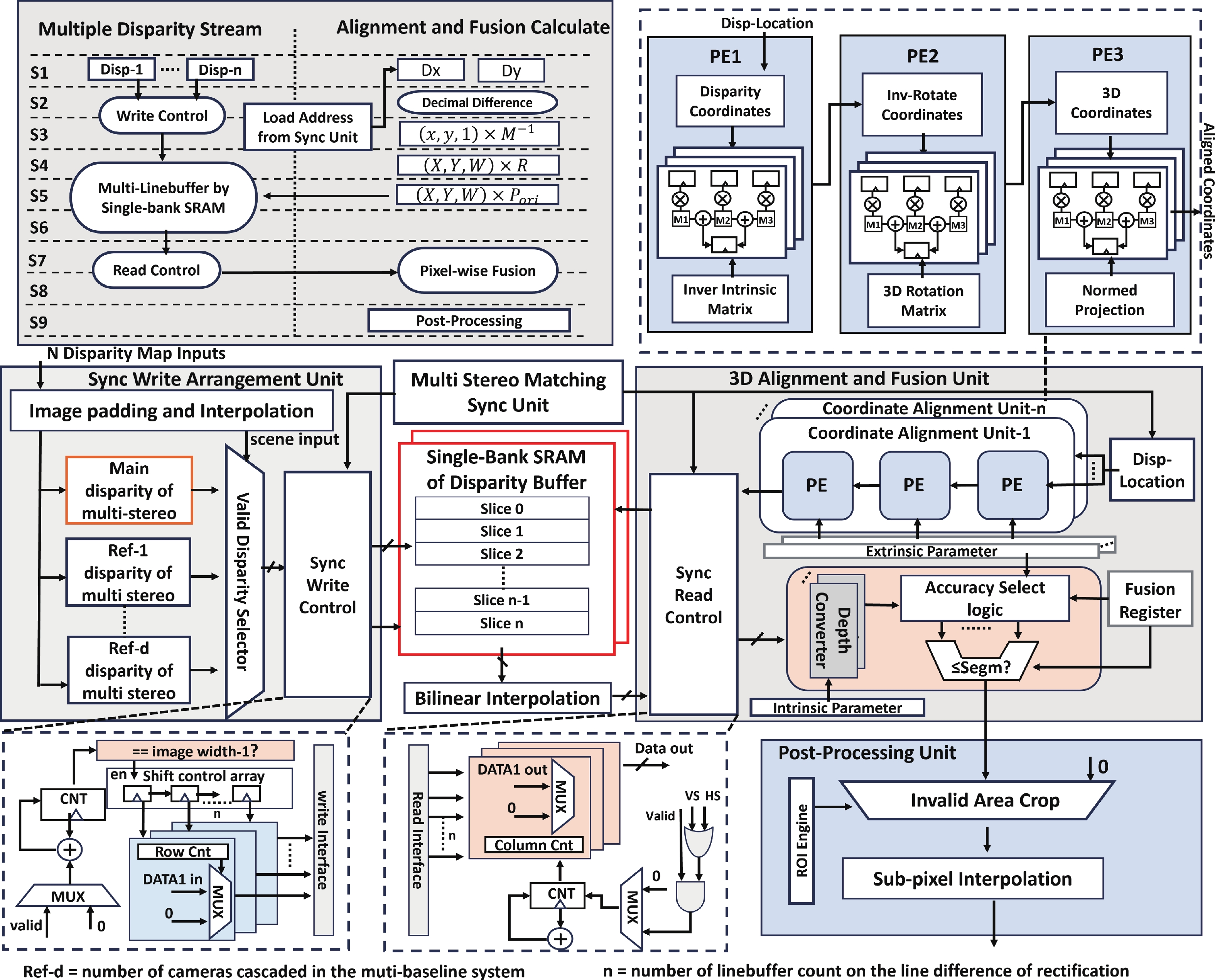
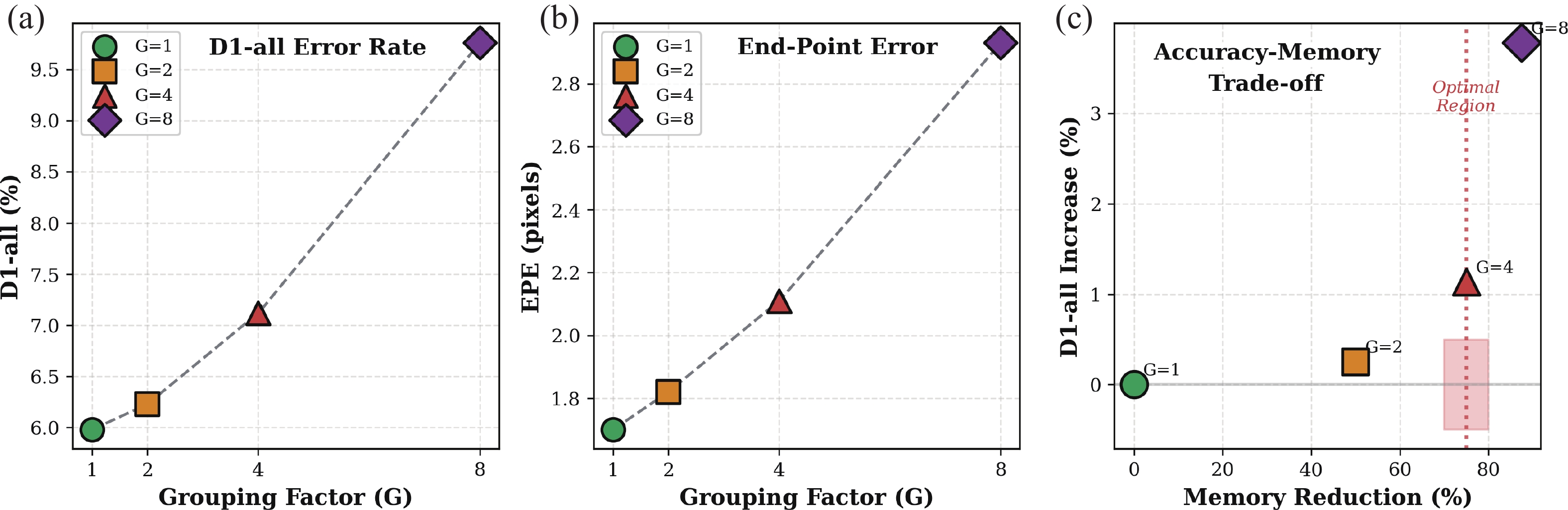
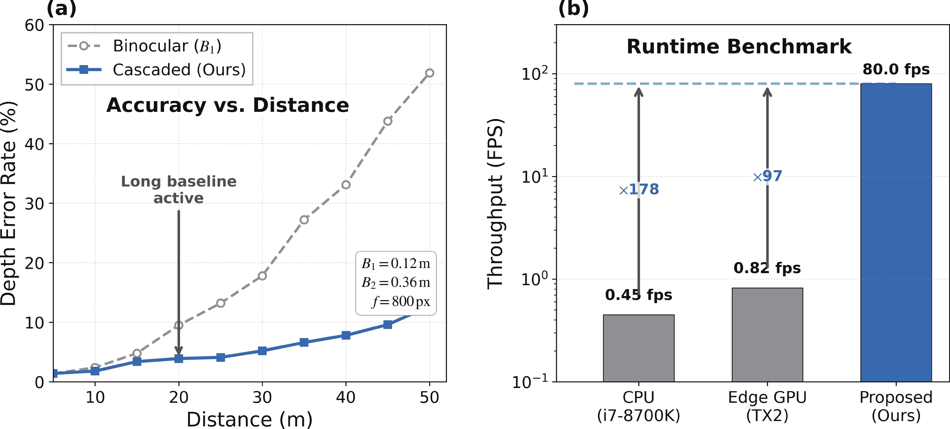
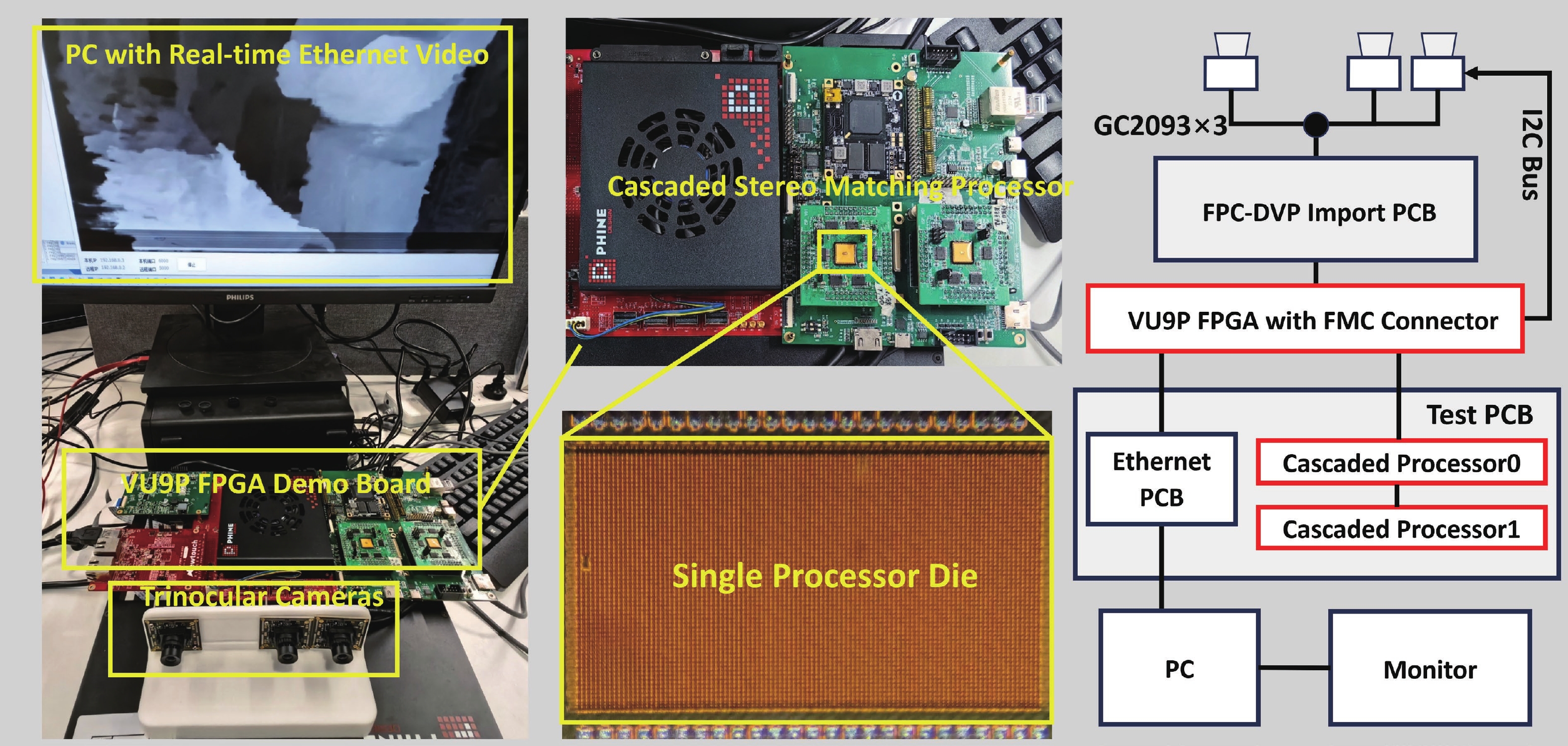
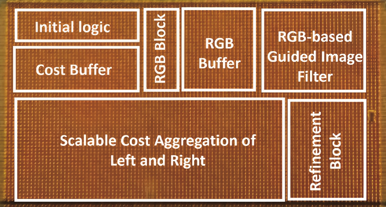
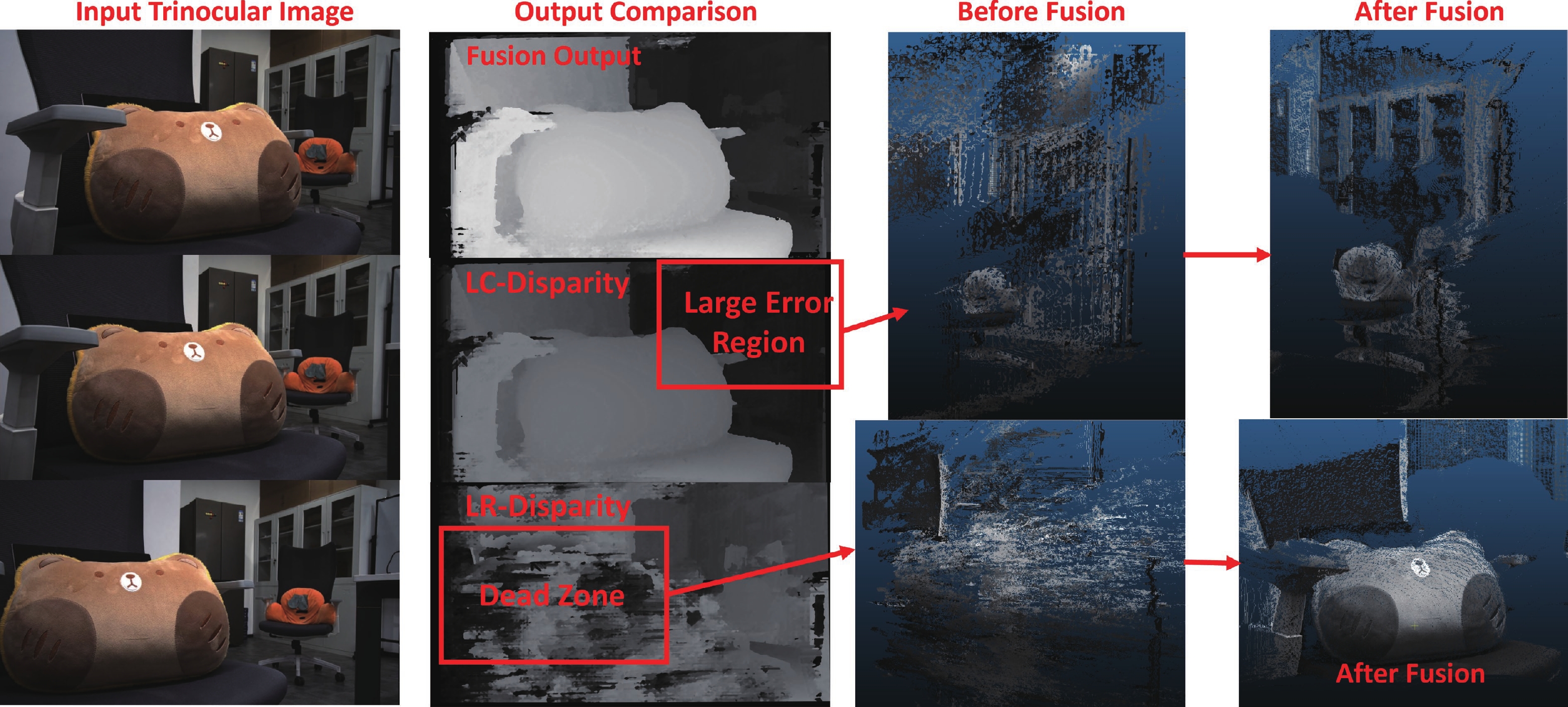
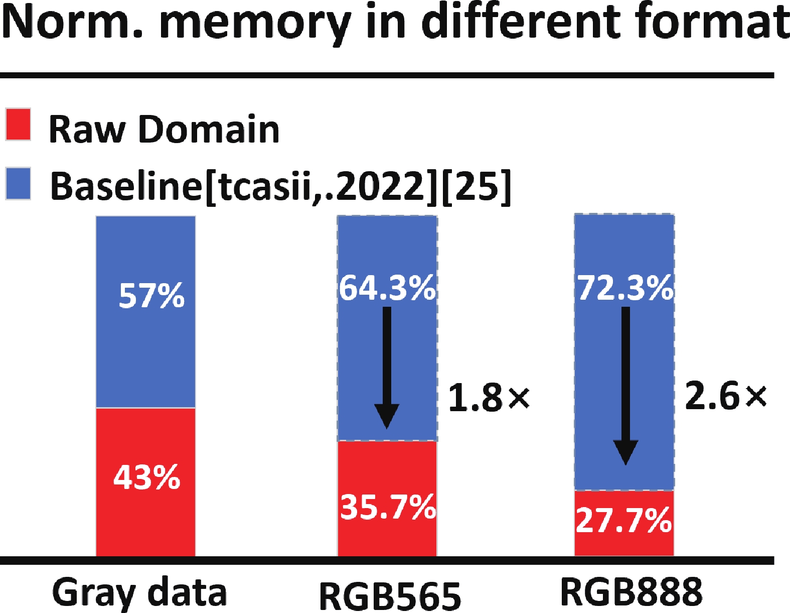
Achieving long-range, high-accuracy depth perception under stringent power constraints remains a critical challenge for stereo vision in edge applications. This work presents a cascadable stereo matching processor that overcomes the inherent trade-off between sensing range and computational efficiency. The core innovation is a scalable semi-global matching (SSGM) algorithm which dynamically optimizes the disparity search range for different baselines, ensuring constant on-chip memory usage and a significant reduction in data movement. The architecture further integrates a raw-domain rectification front-end, which performs direct geometric transformation on Bayer-patterned image streams. This approach eliminates the need for external memory access by bypassing conventional ISP pipelines, thereby maximizing throughput and reducing system memory consumption. Parallel processing paths for multiple baselines converge in a pixel-wise fusion module, which synthesizes a unified depth map by selecting the most reliable disparity estimate for each output pixel. The cascadable stereo matching processor achieves speedups of up to 178x and 97x over CPU and EdgeGPU platforms, respectively, in multi-baseline stereo disparity fusion. Implemented in 40-nm CMOS technology, the processor operates at 160 MHz, achieving a processing speed of 80 frames per second with an energy efficiency of 7.9 pJ/pixel and occupying a core area of 6.04 mm2.
J. Semicond.
2026, 47(6): 062204 doi: 10.1088/1674-4926/26010040
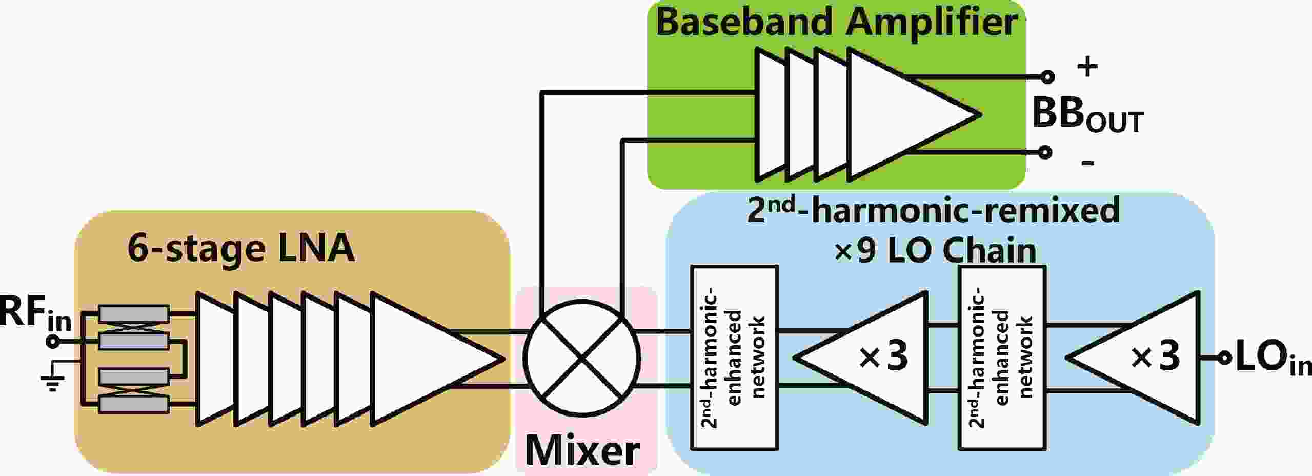
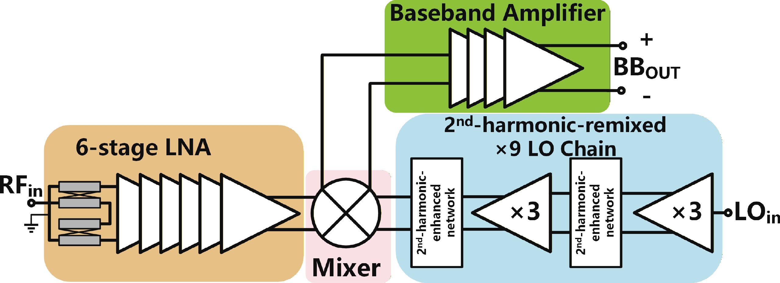
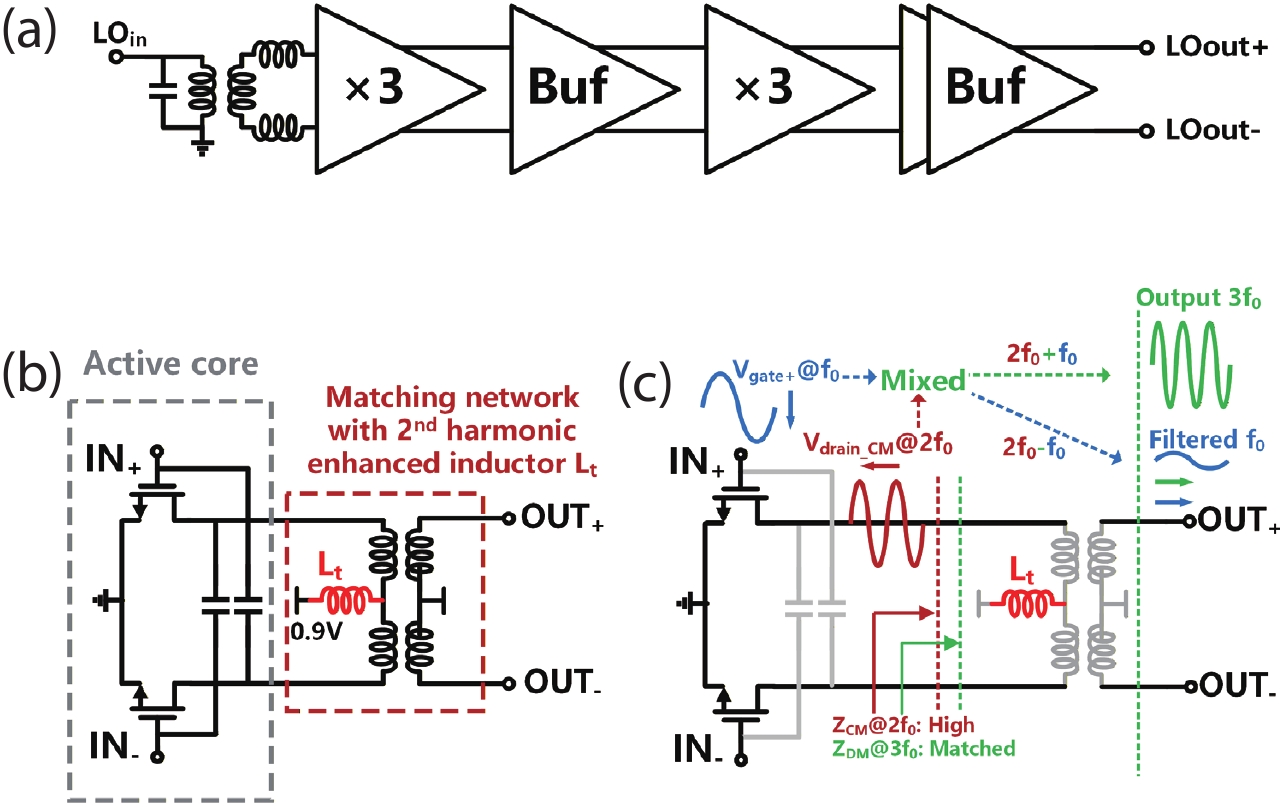
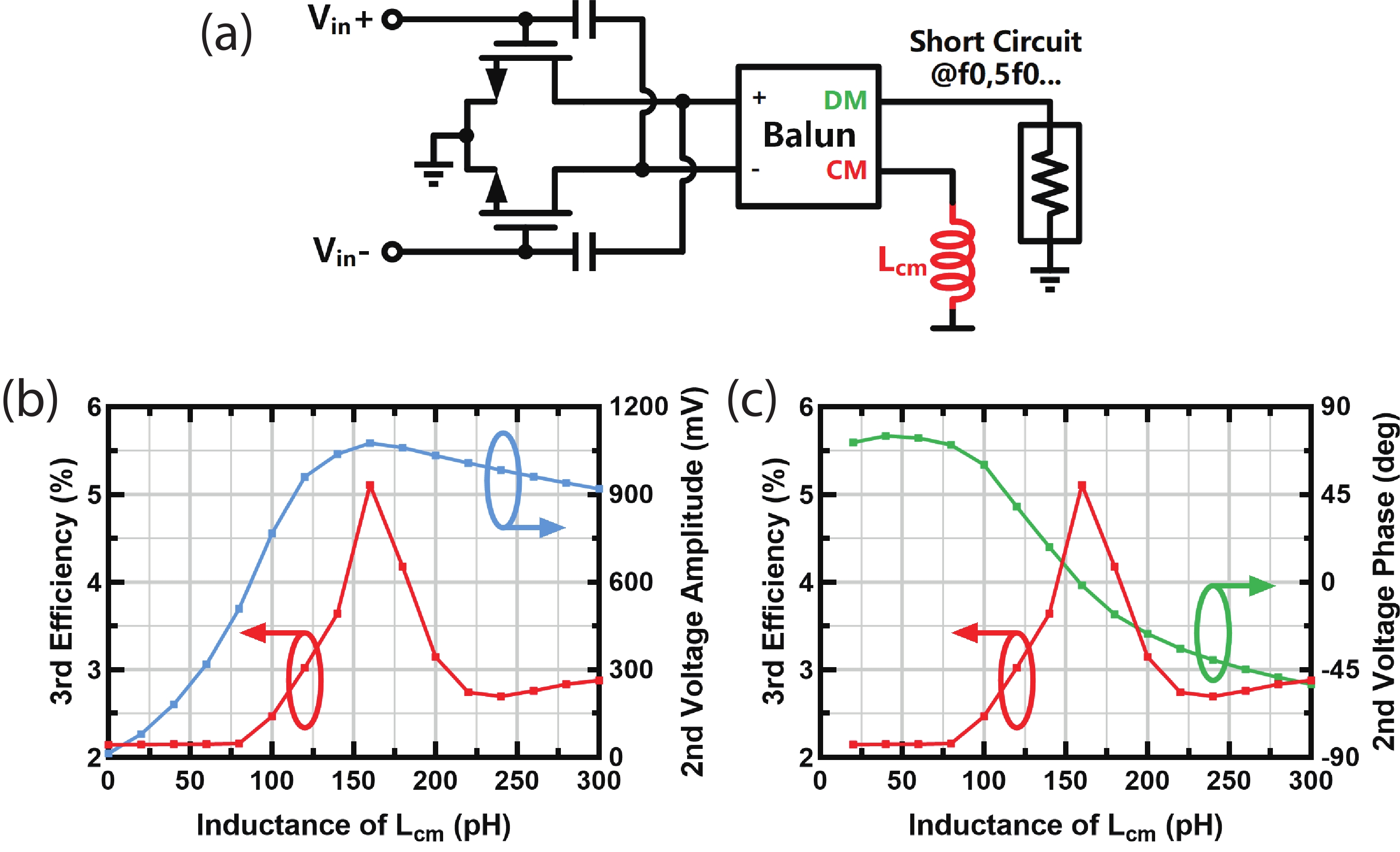
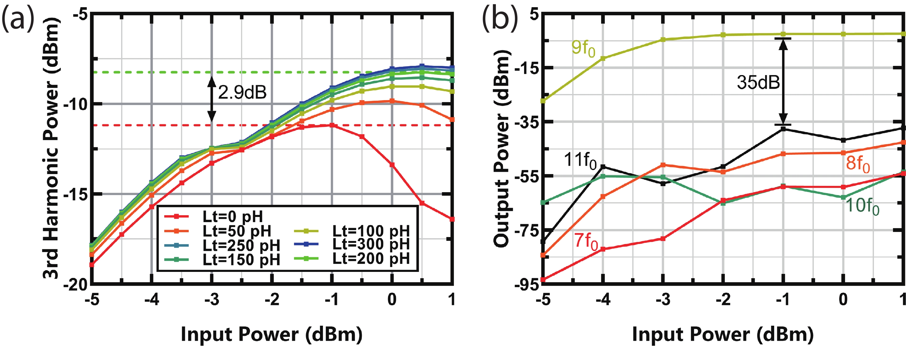
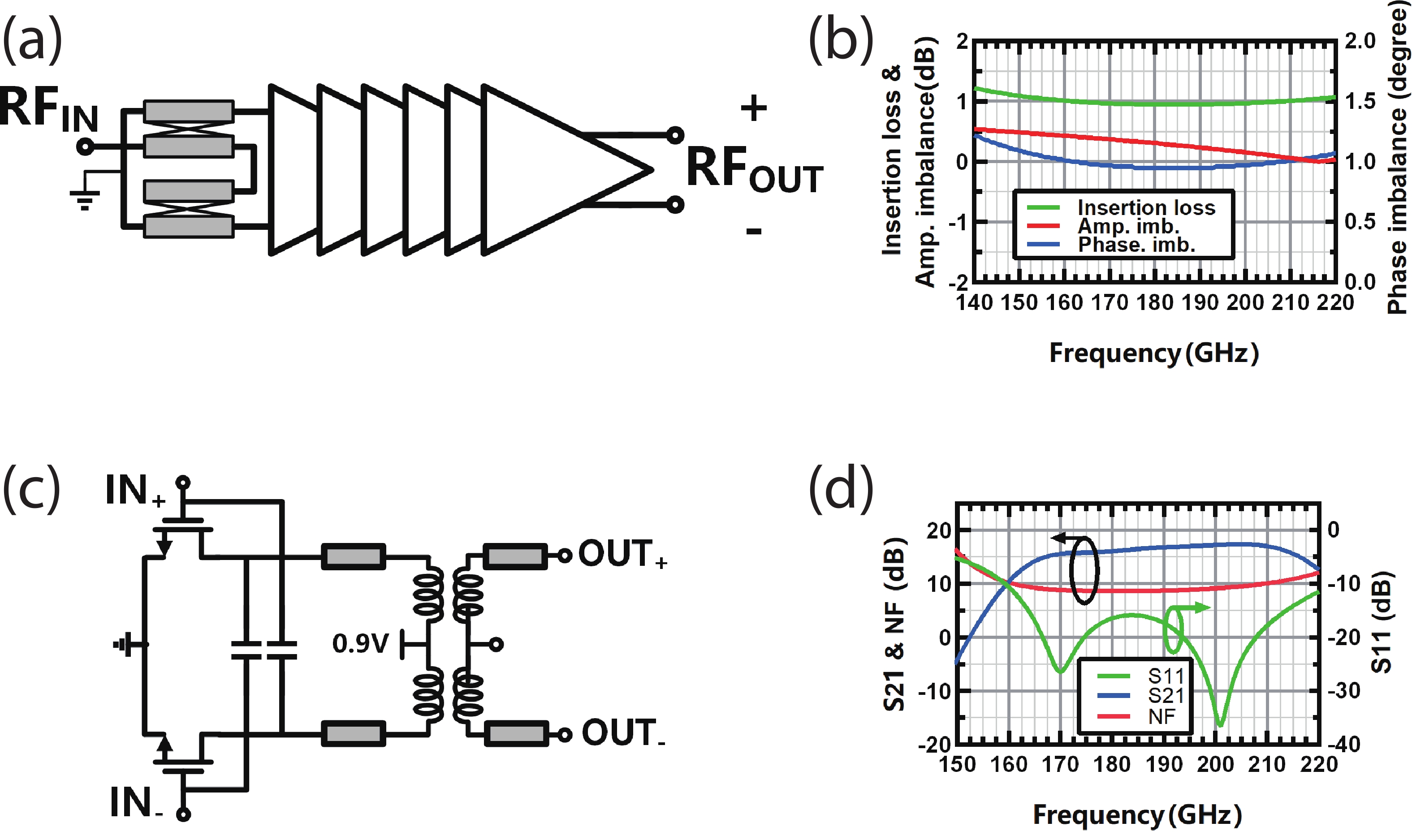
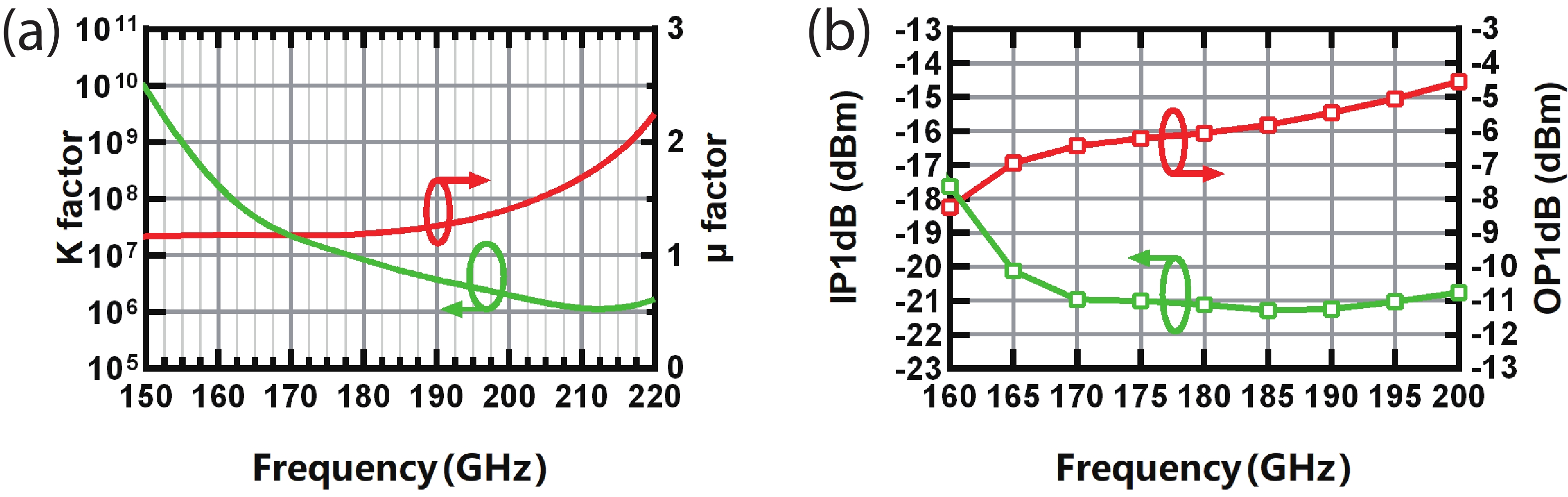
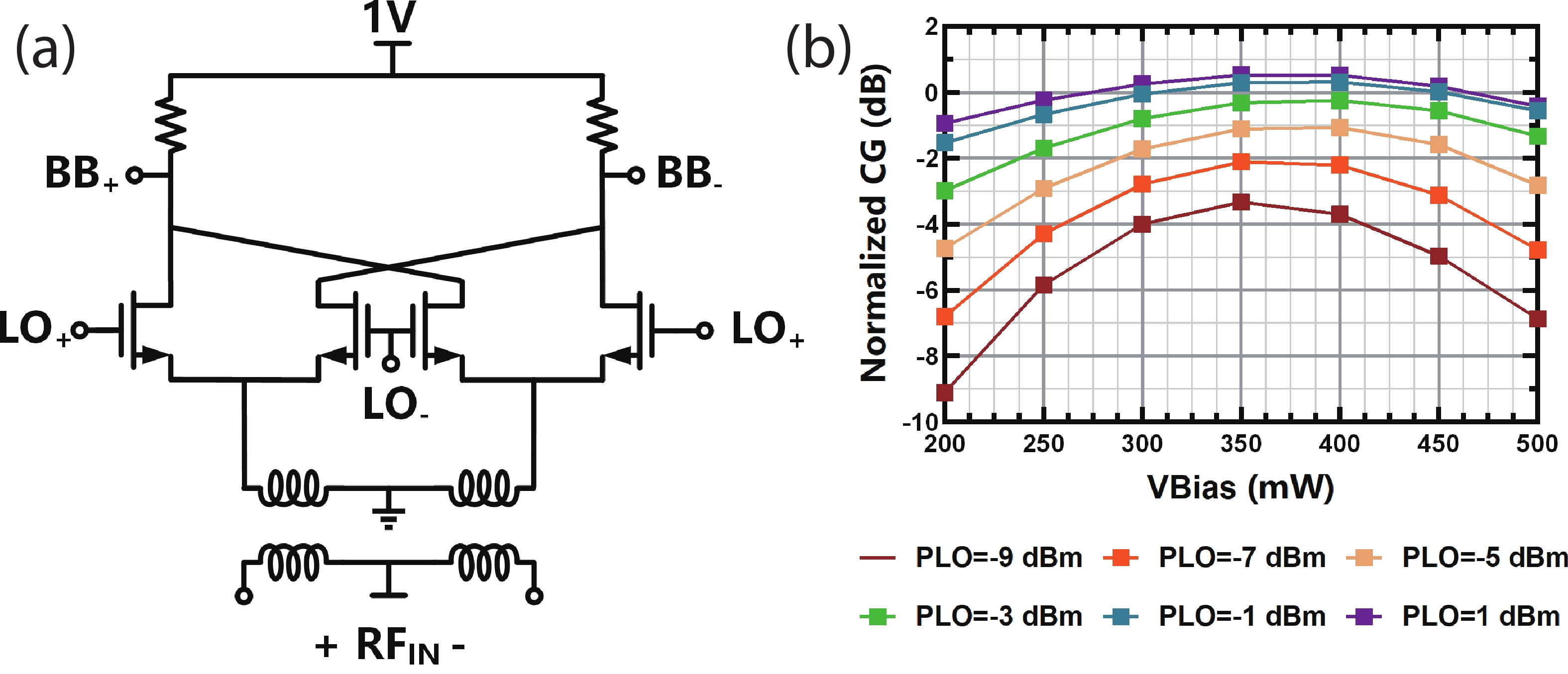
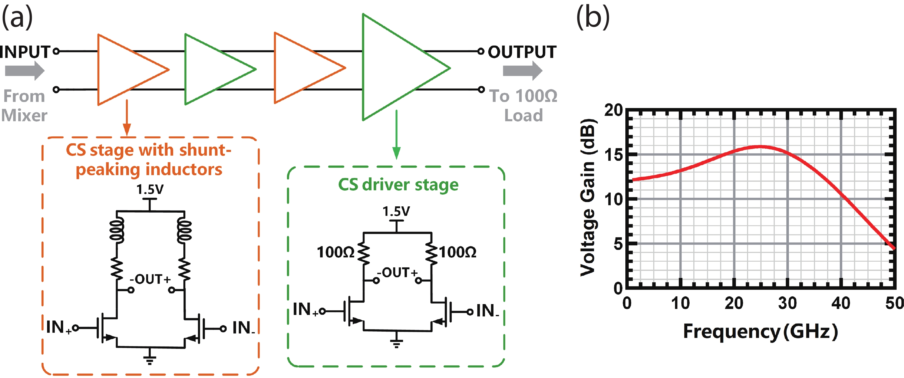
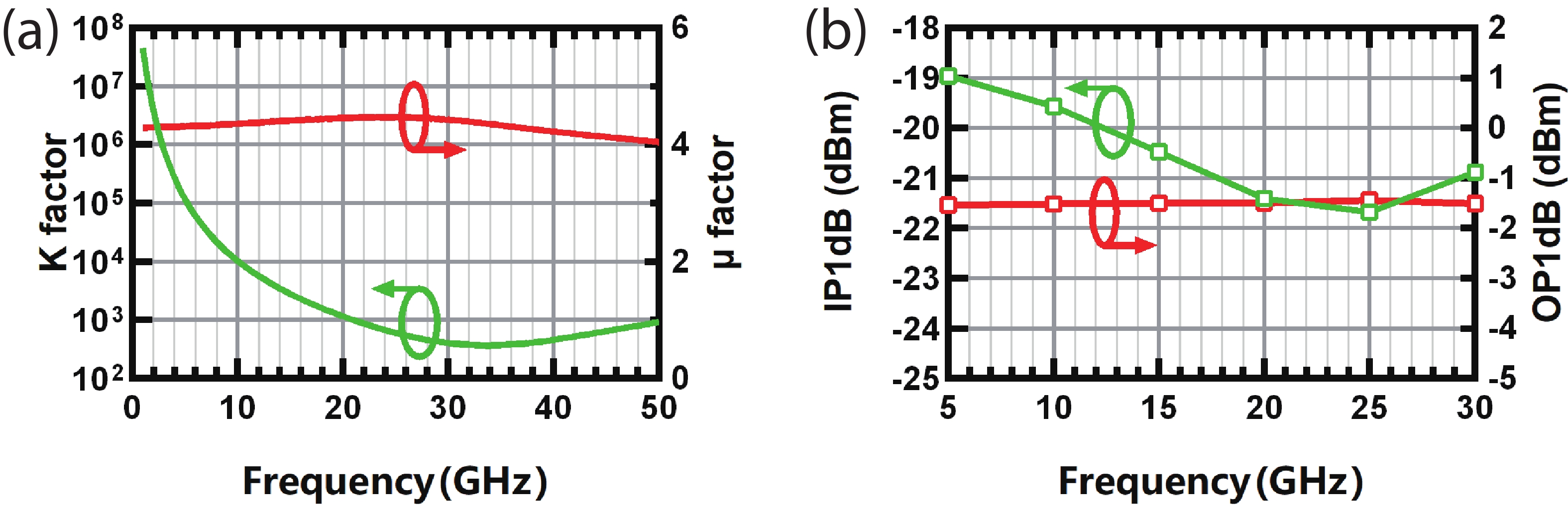
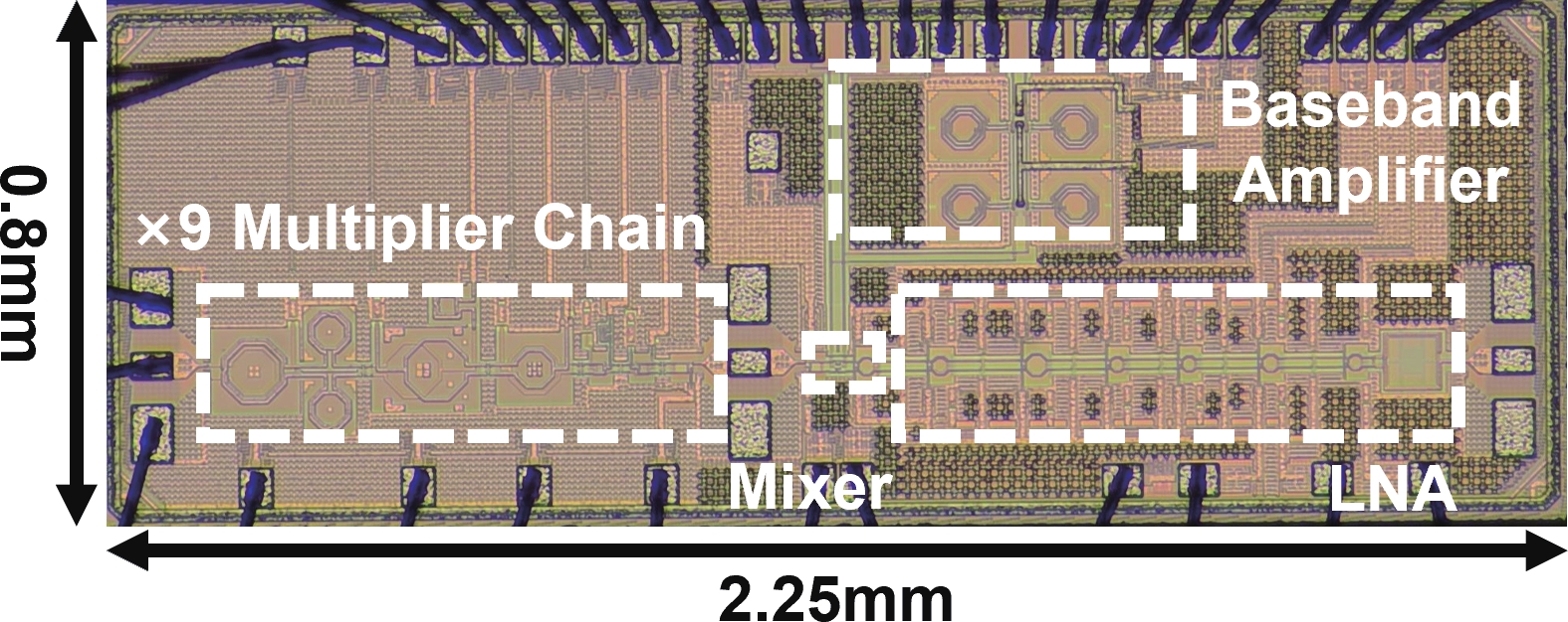
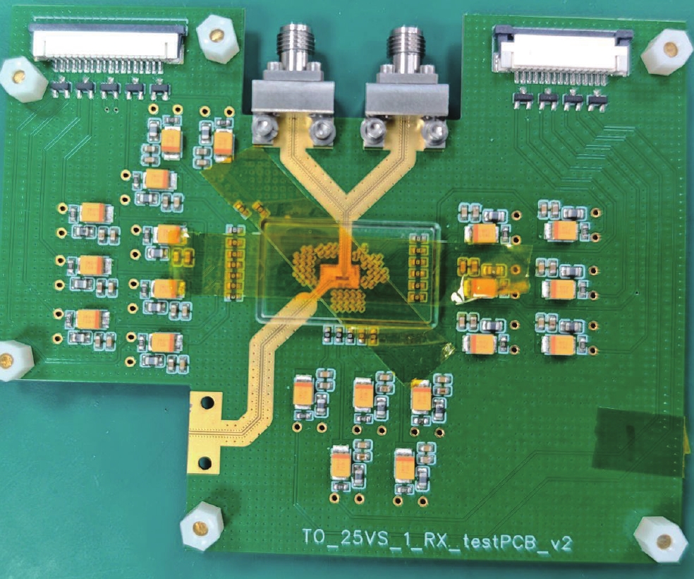
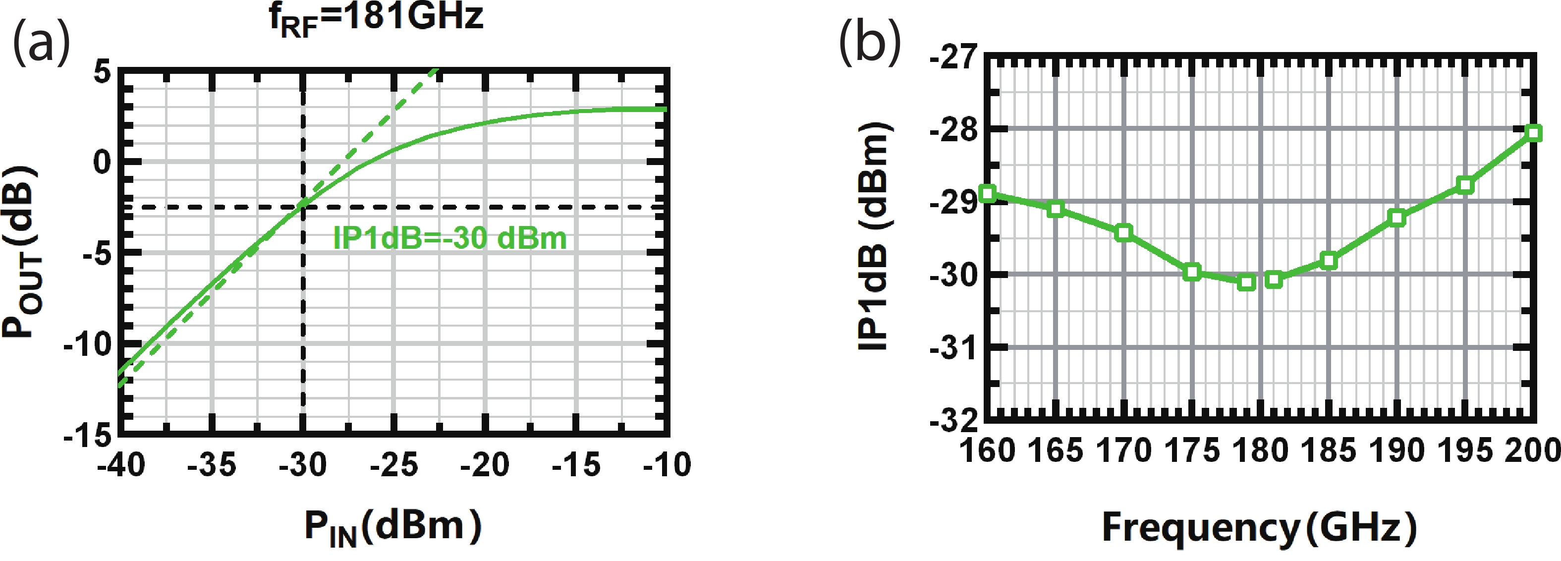
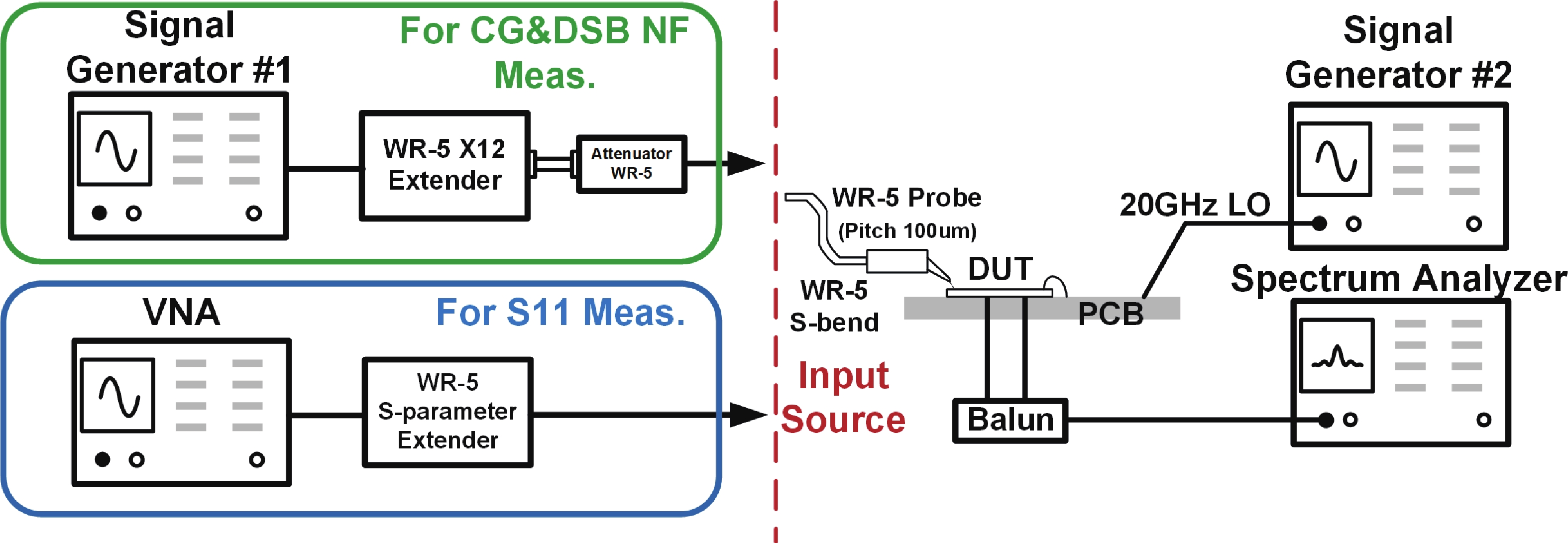
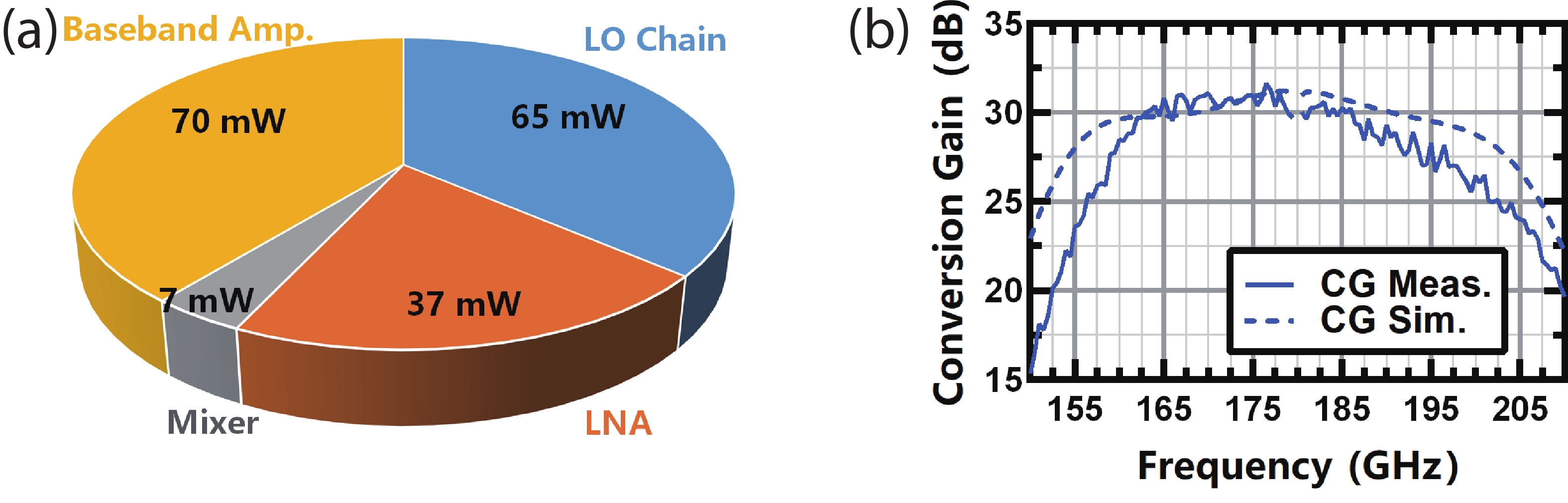
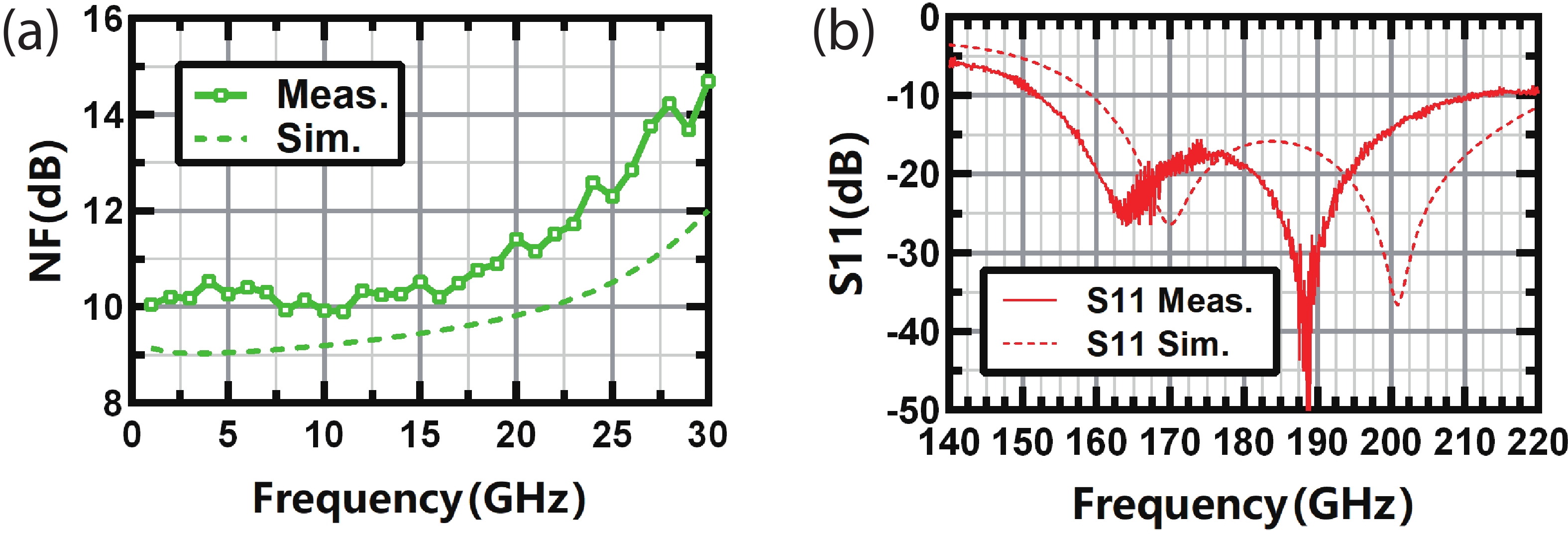
In this paper, a compact and low-power sub-THz direct-conversion receiver with a second-harmonic-remixed LO chain is proposed. Based on a common-mode second-harmonic-enhanced network, the common-mode second-harmonic voltage at the drains of the common-source differential pair in the tripler is enhanced and mixed with the fundamental voltage at the gate to generate additional differential third-harmonic voltage. Hence, the saturation output power and efficiency of the triplers used in the LO chain have been significantly improved. The power consumption of the LO chain employed in the receiver is as low as 65 mW. Measurement results demonstrate that the receiver achieves a conversion gain of 30.5 dB and a 3-dB RF bandwidth of 34 GHz, while the in-band minimum noise figure is 9.9 dB.
J. Semicond.
2026, 47(6): 062301 doi: 10.1088/1674-4926/25100024
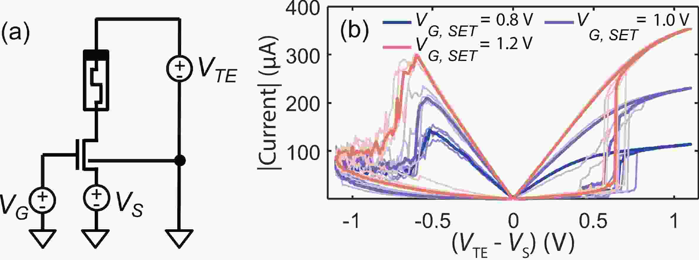
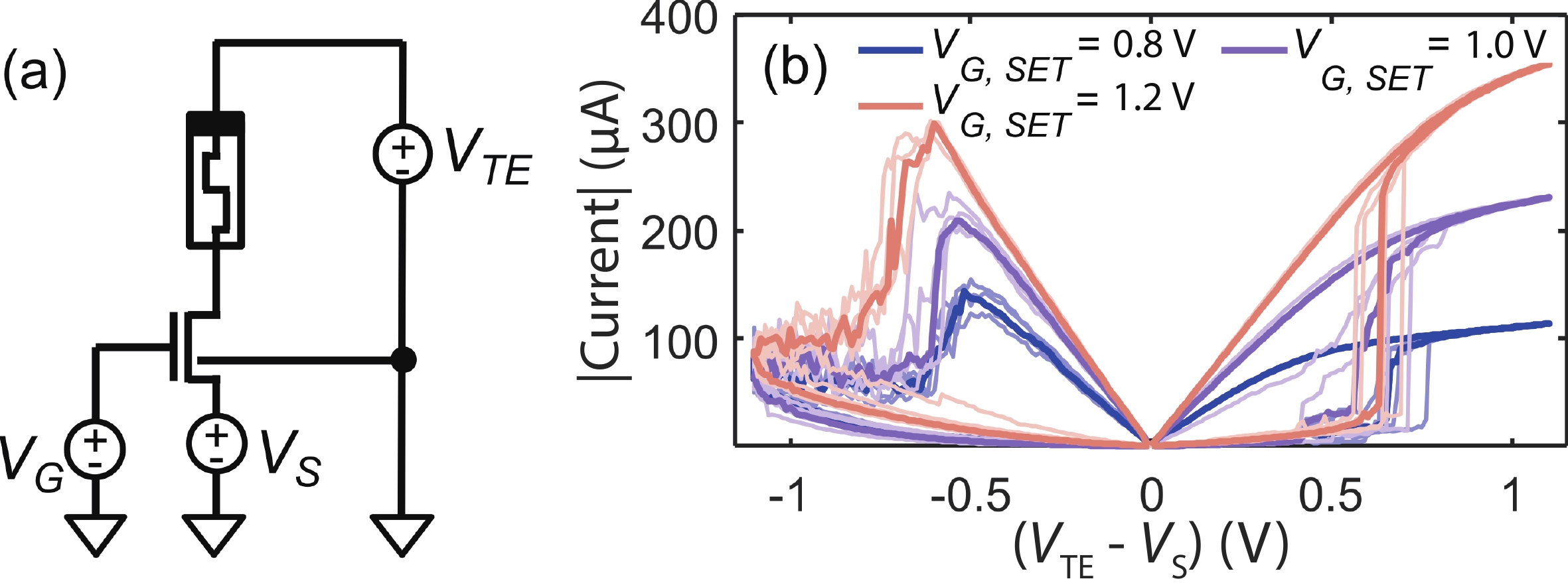
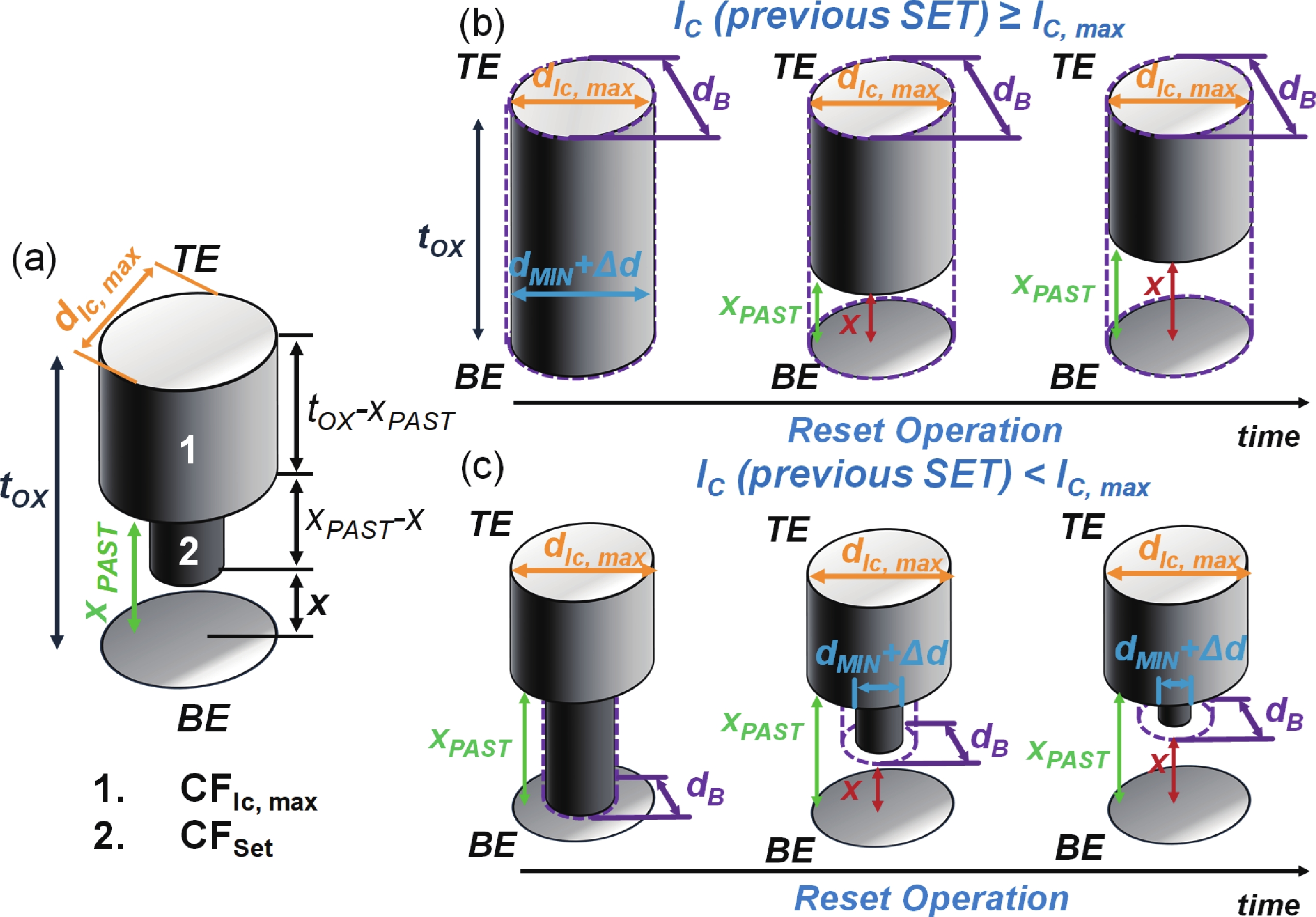
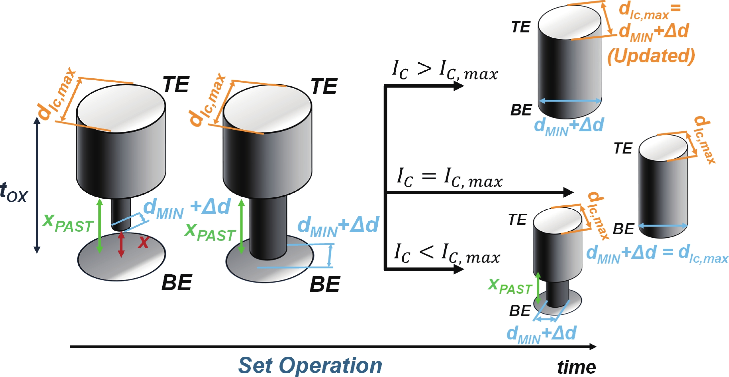
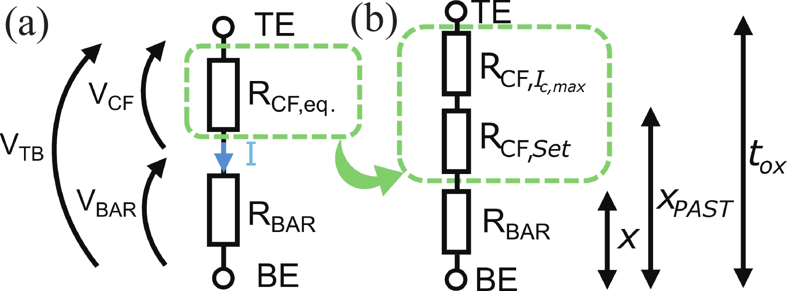
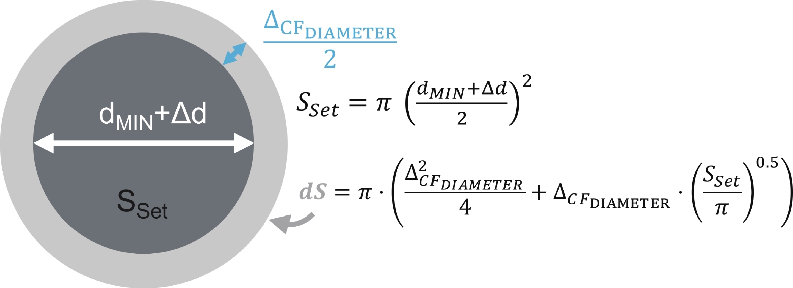
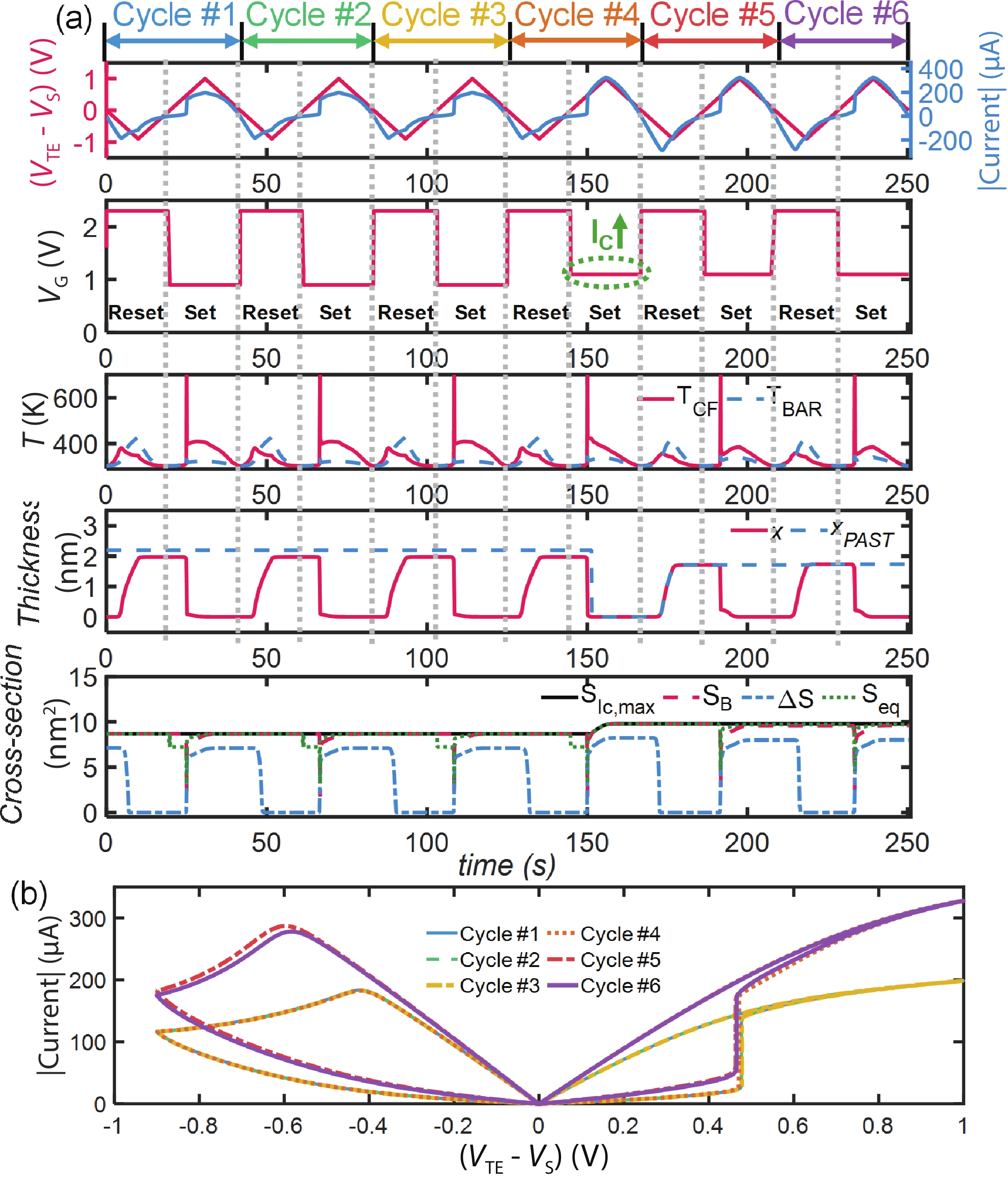
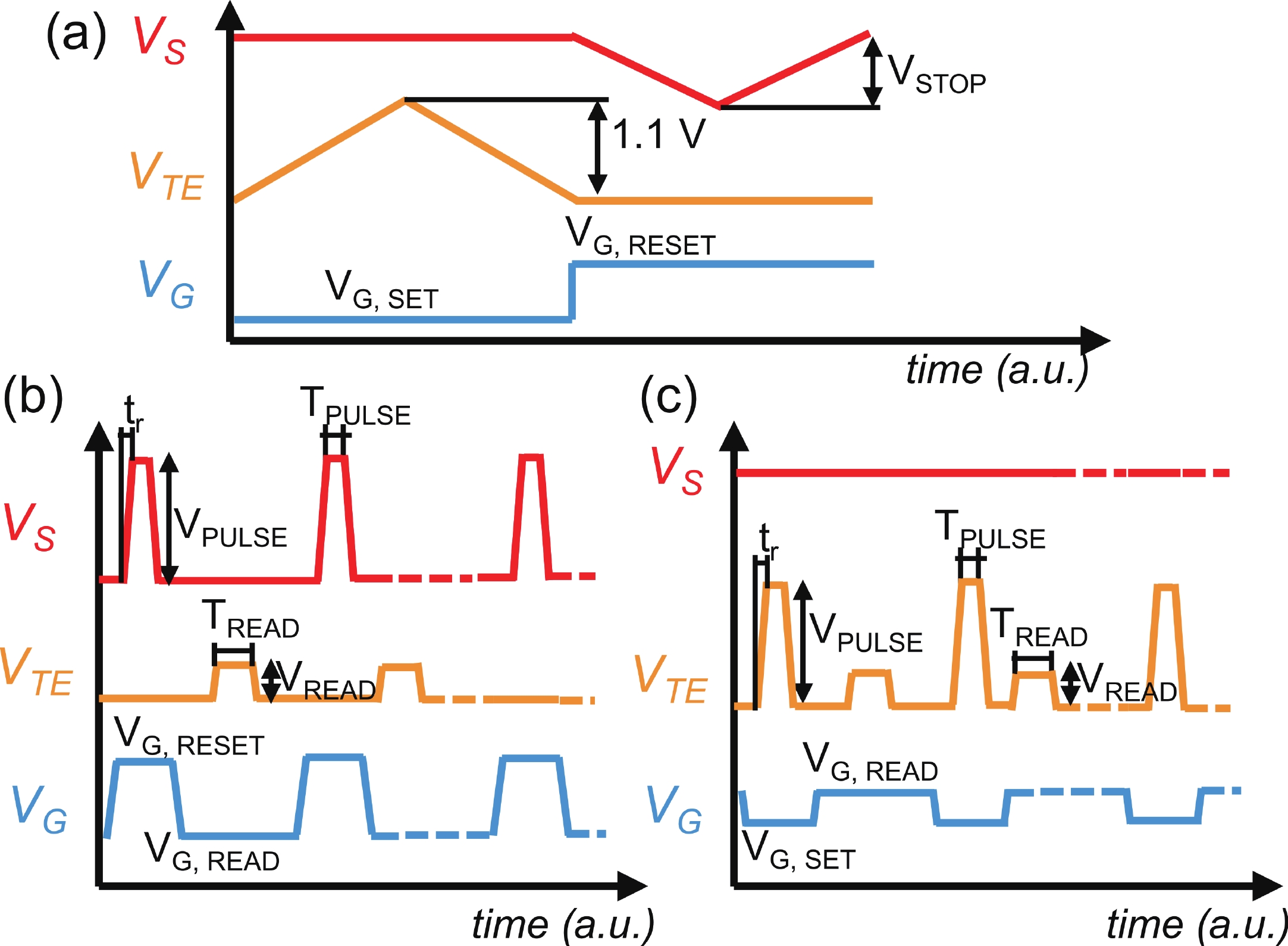
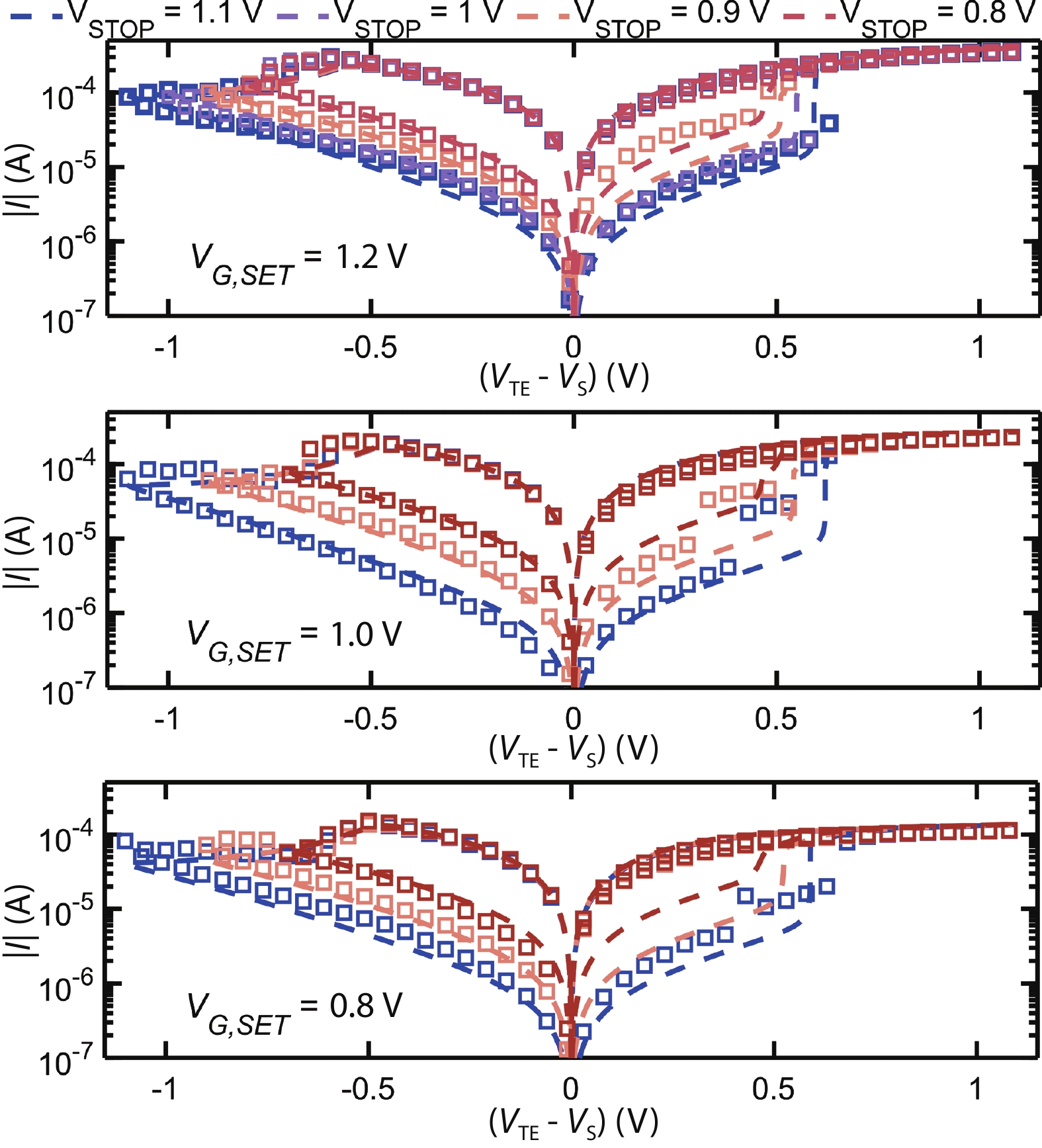
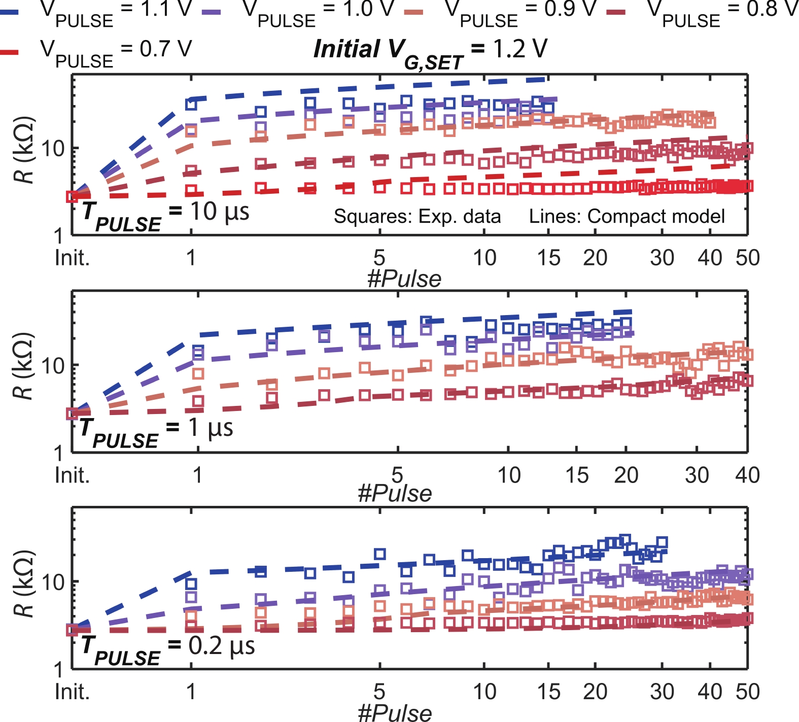
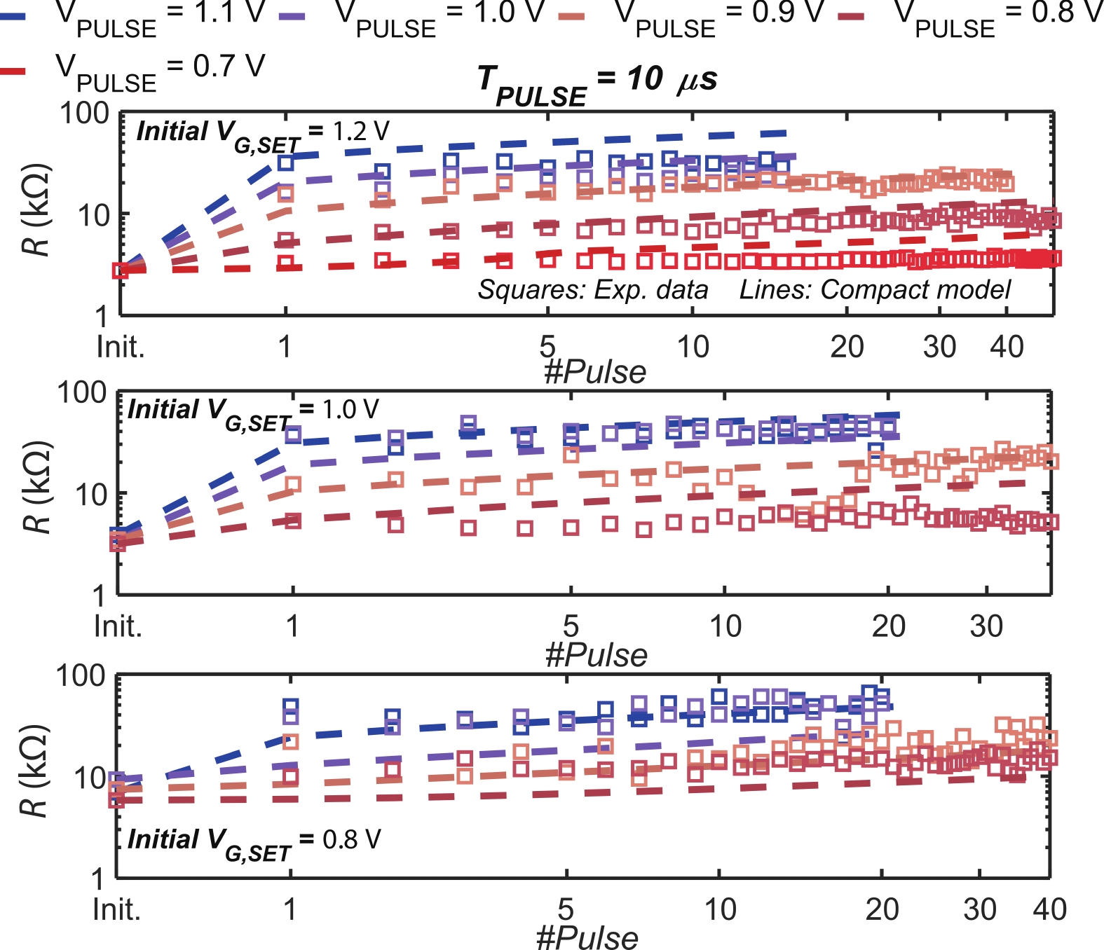
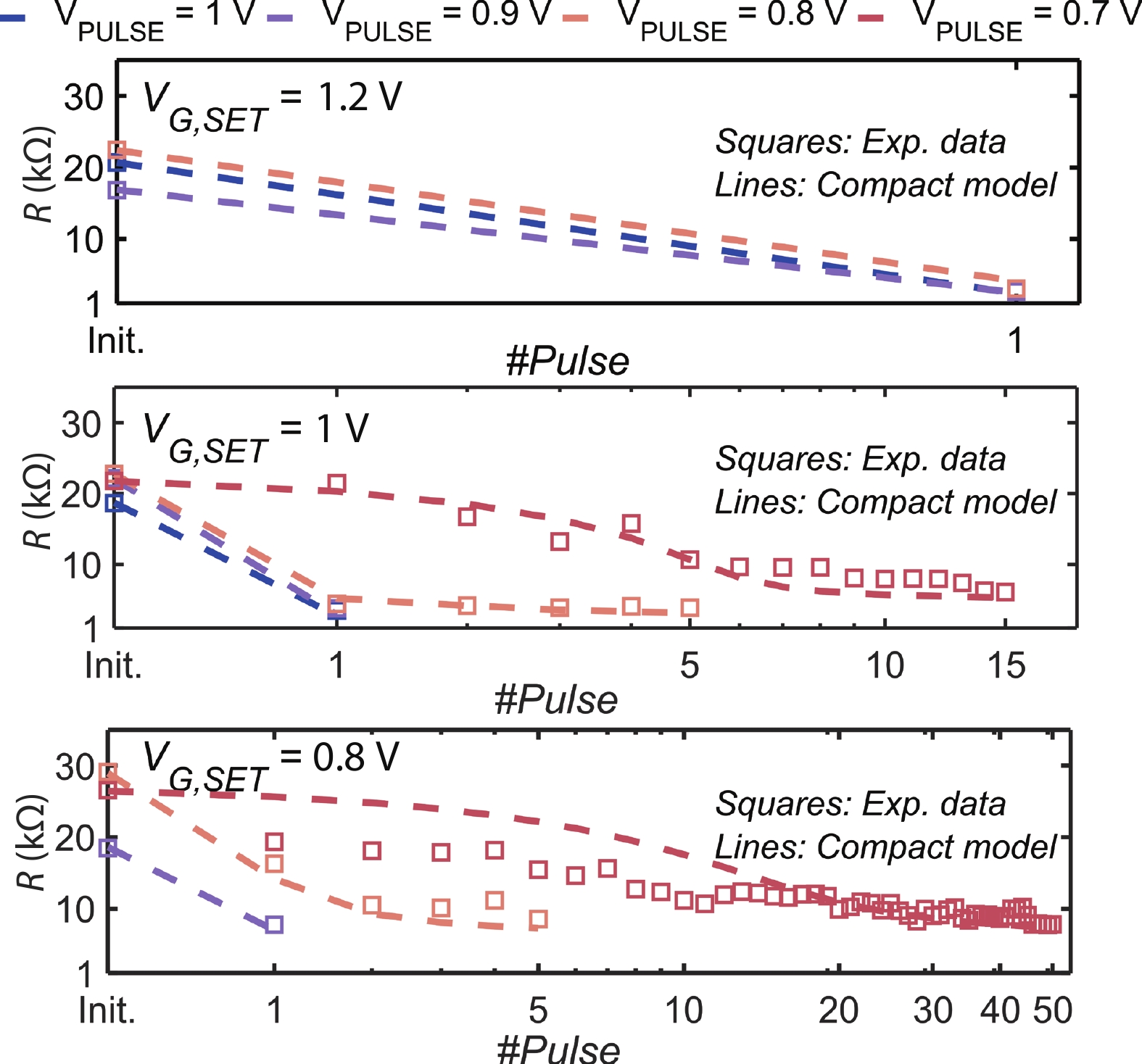
Resistive random access memories (RRAMs) are emerging as a key enabling technology for cost-effective, energy-efficient and secure chips, especially in the framework of edge computing. In particular, their electrically programmable resistance has been widely exploited in several in-memory computing and neuromorphic architectures. By adjusting the applied voltages and compliance currents (IC), RRAM devices can be programmed to multiple resistance states during set and reset procedures, enabling multilevel functionality. While the multilevel behavior of the reset phase is generally well captured by existing compact models, only a few account for the multilevel characteristics of the set operations. Moreover, such models are rarely validated against comprehensive experimental datasets capturing device dynamics across multiple timescales. In this work, we present a physics-based compact model that enhances the UniMORE RRAM framework by incorporating the dynamic lateral evolution of the conductive filament (CF), thereby enabling accurate simulation of set operations at varying IC values. The model is calibrated to experimental data from IHP 130 nm 1T1R RRAM technology and reproduces device behavior across several operating conditions using a single set of parameters. The results highlight the potential of the proposed compact model in design optimization workflows of RRAM-based circuits.
J. Semicond.
2026, 47(6): 062302 doi: 10.1088/1674-4926/25100005

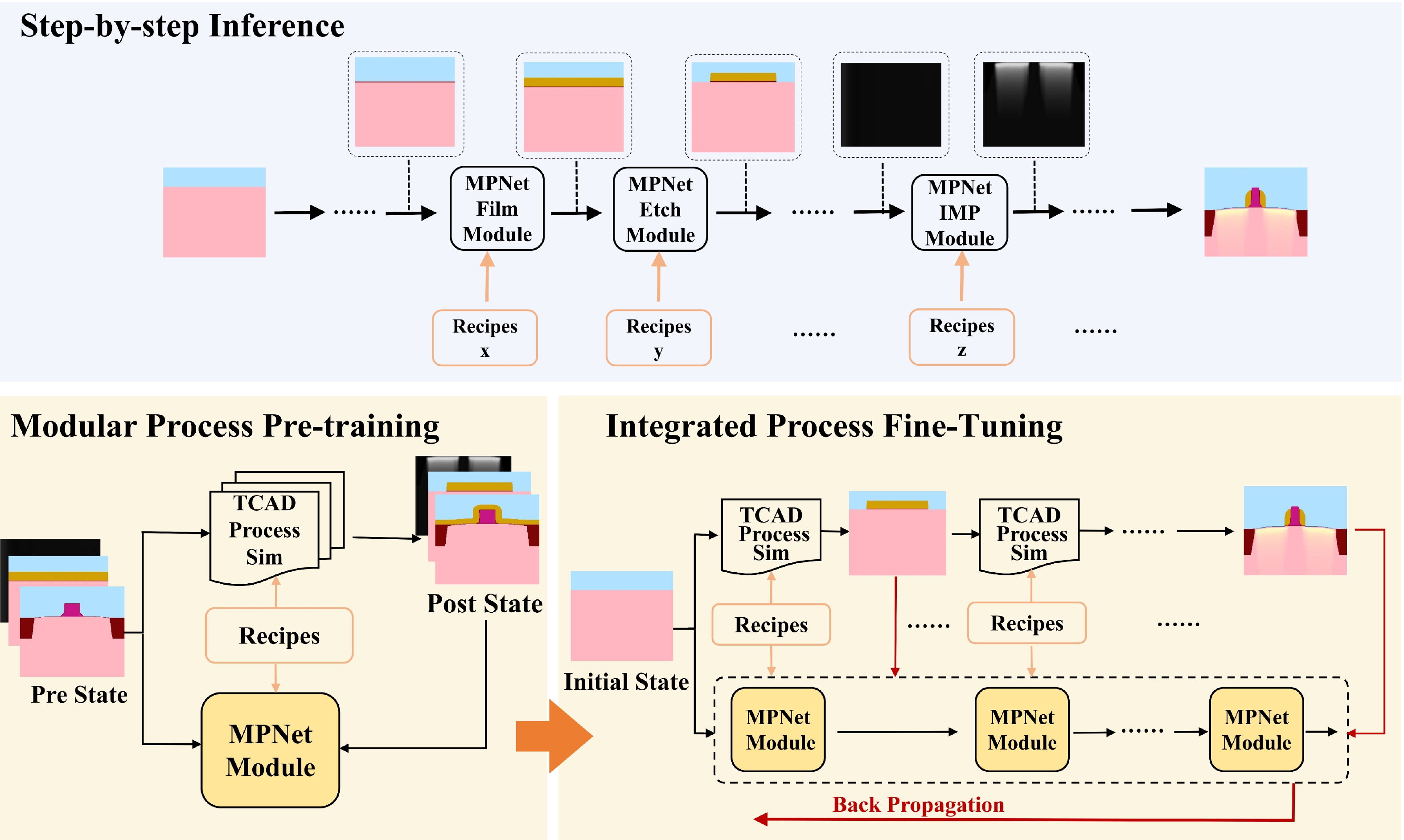
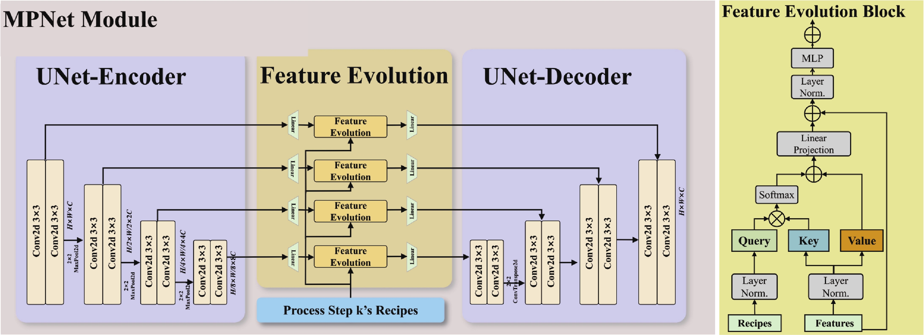
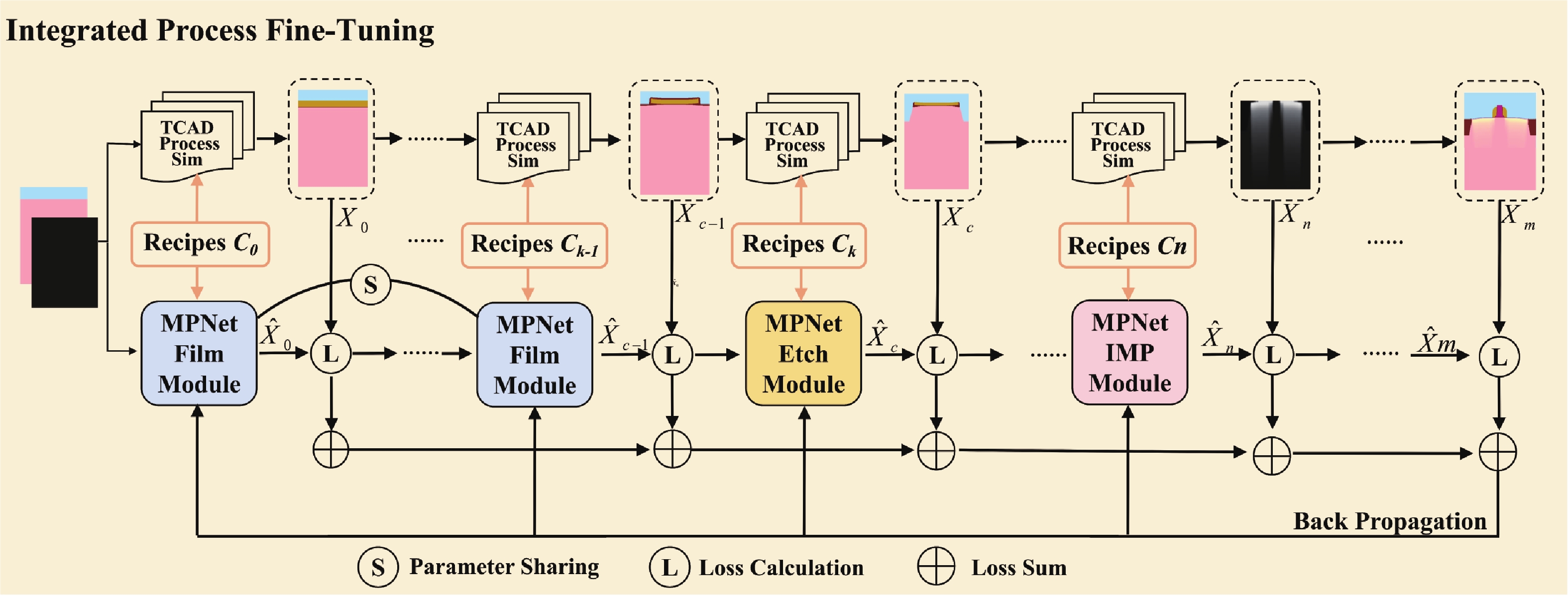
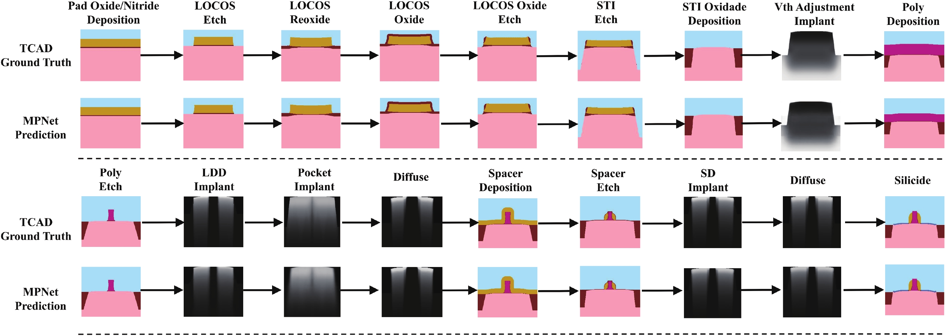
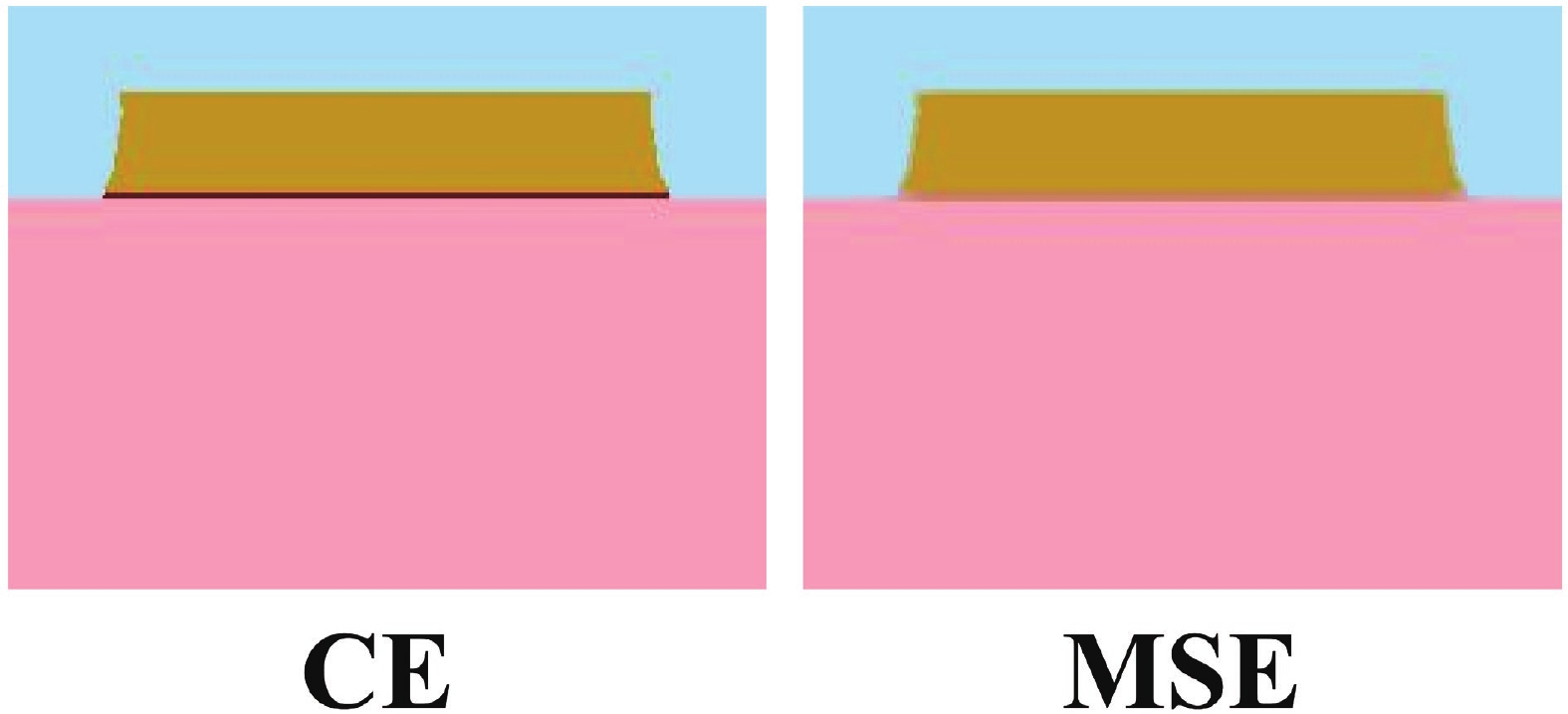
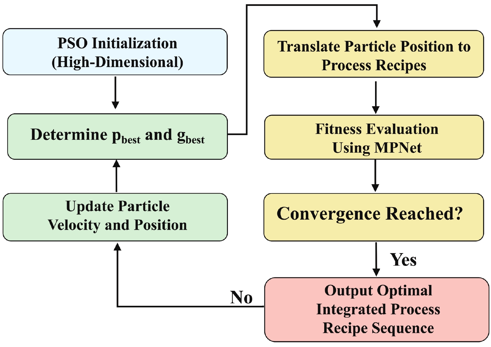
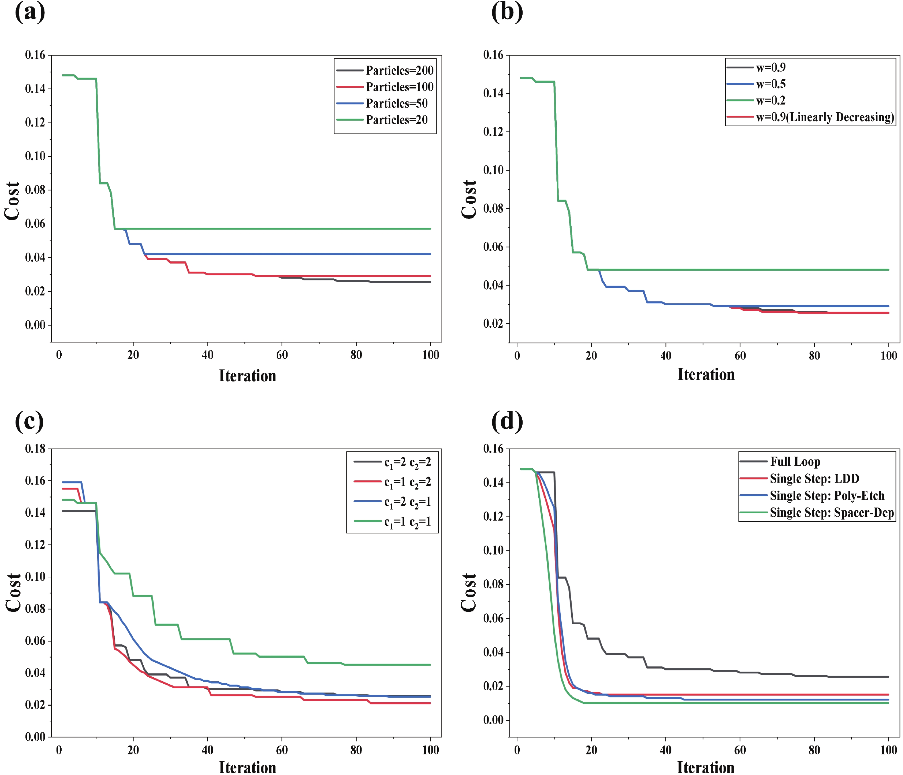
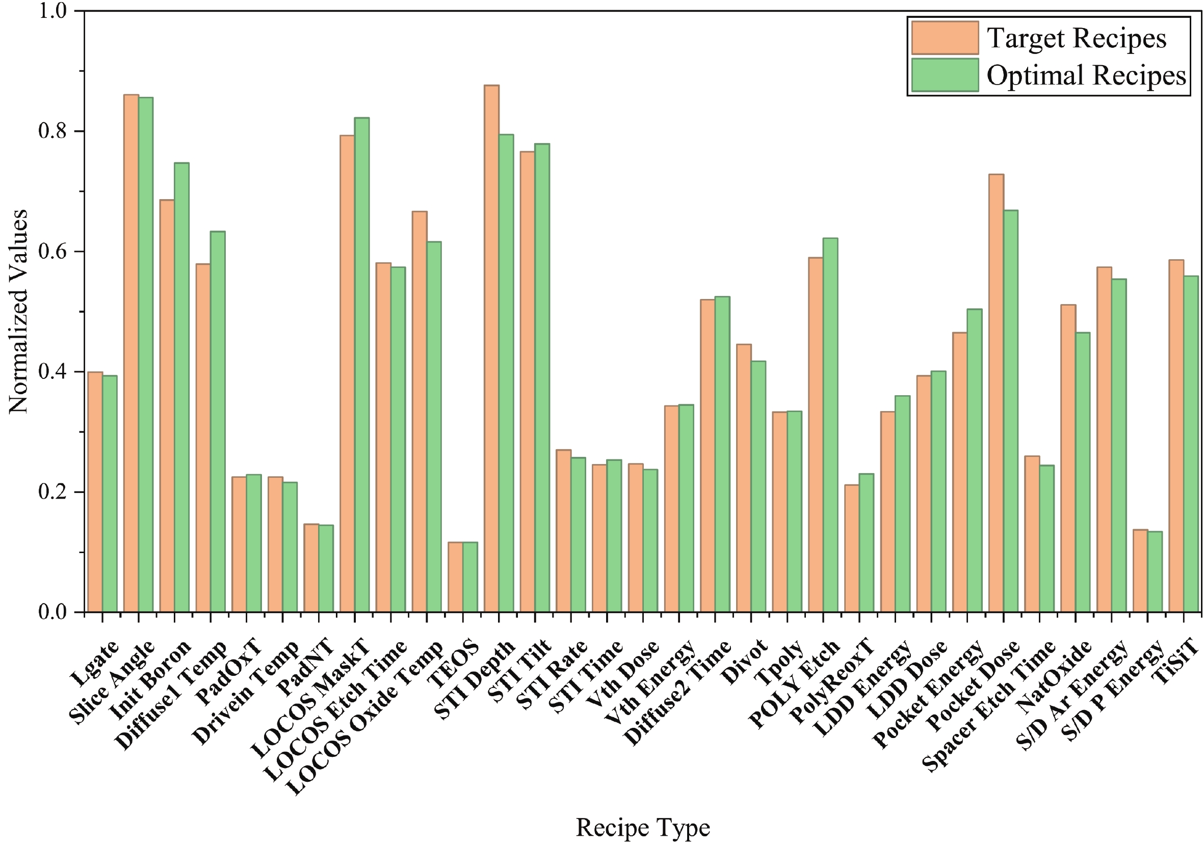
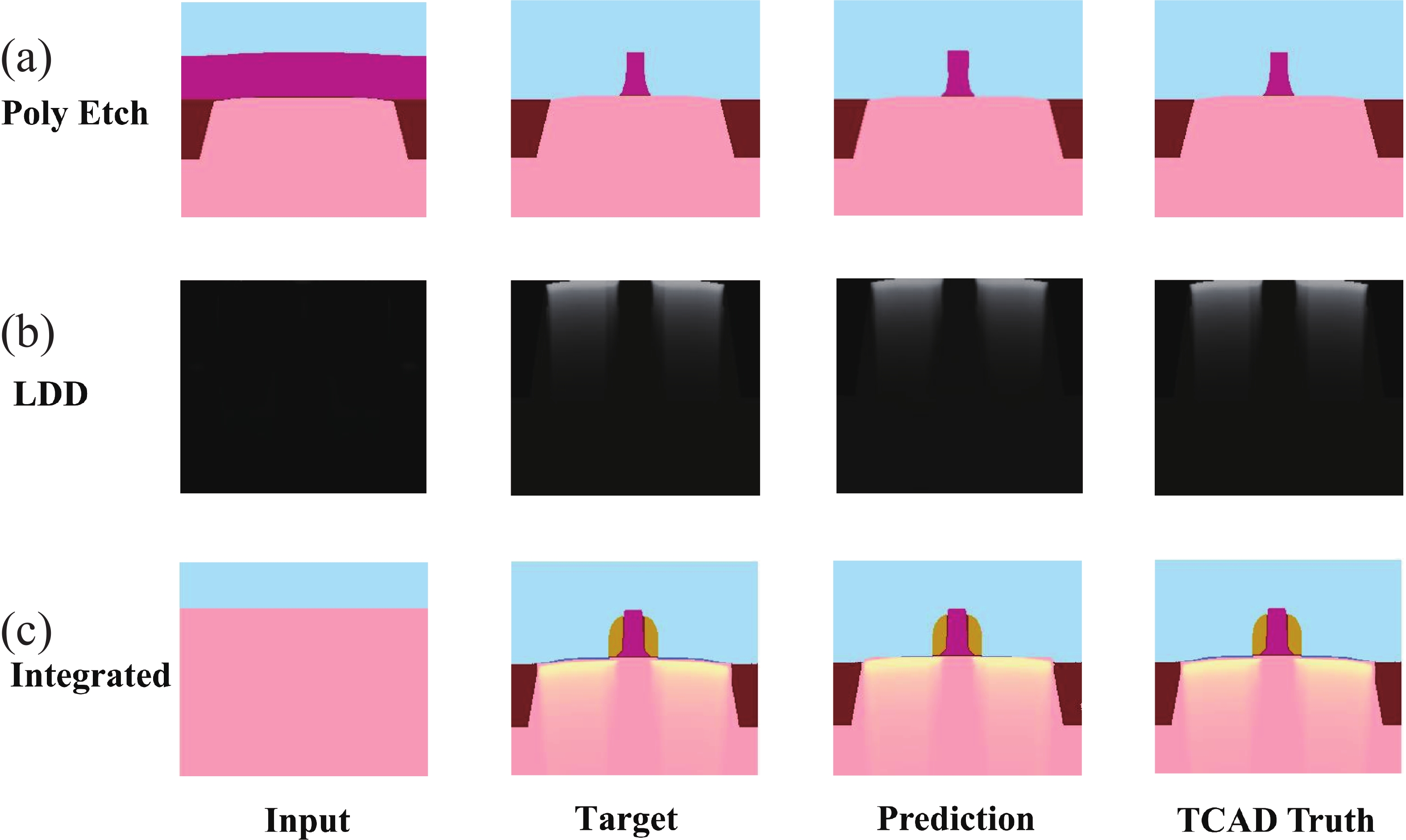
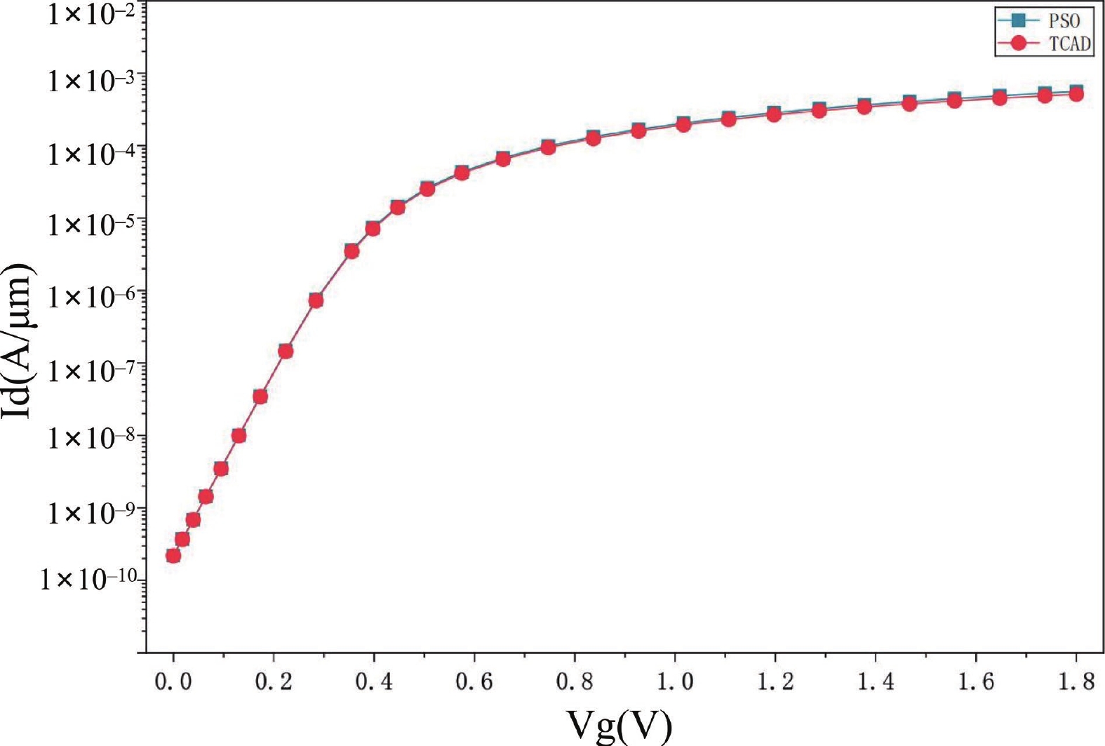
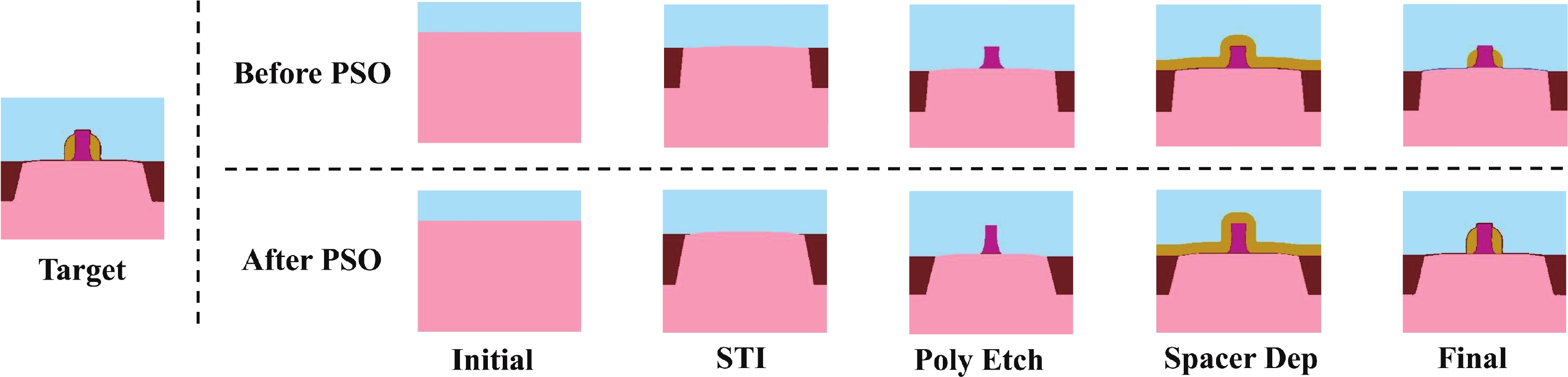
The computational cost of TCAD simulations is becoming prohibitively high with the complexity of advanced process technologies, making simulation acceleration a critical research priority. While end-to-end surrogate models mapping process recipes to device structures and characteristics offer a promising alternative, their application is often limited by poor generalizability and explainability. In this work, we present MPNet, a modular deep learning surrogate modeling framework for process TCAD. MPNet comprises distinct surrogate models for individual process modules, which are assembled into an integrated framework. These modular models employ a novel UNet-attention feature evolution method to capture the complex evolutions of device geometry and doping profiles. Each module can be trained separately on its individual process, after which the modules are cascaded and jointly fine-tuned to minimize error accumulation throughout the cascade. The efficacy of the proposed MPNet framework is demonstrated through a MOSFET integrated process TCAD case study. Results show that MPNet achieves a computational speedup of over 103 times compared to conventional TCAD, while maintaining predictive fidelity exceeding 98%. Finally, to illustrated the application of the proposed framework, MPNet is coupled with a PSO algorithm, showcasing its utility for fast process optimization to meet specific process targets.
J. Semicond.
2026, 47(6): 062303 doi: 10.1088/1674-4926/25120026
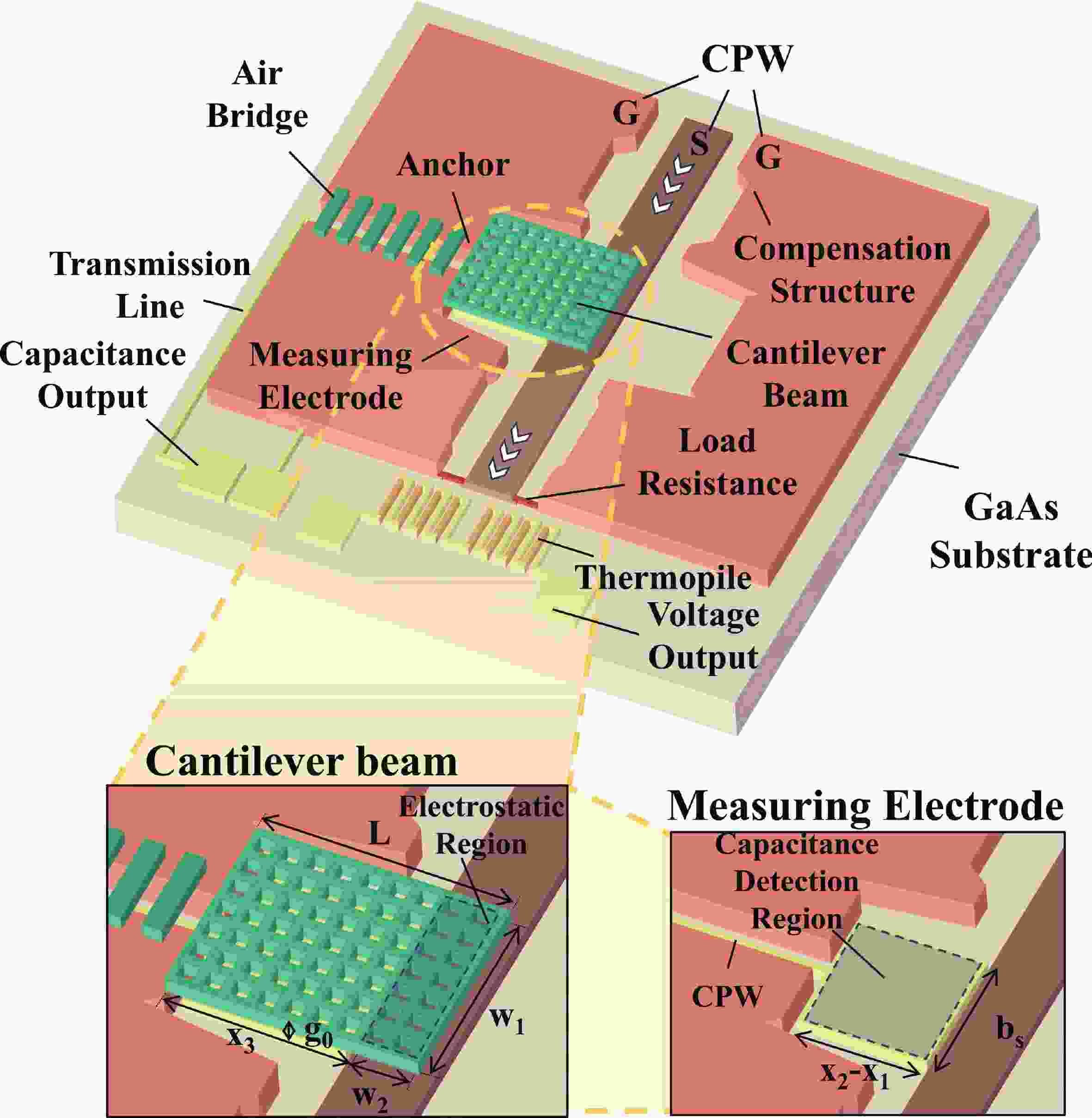
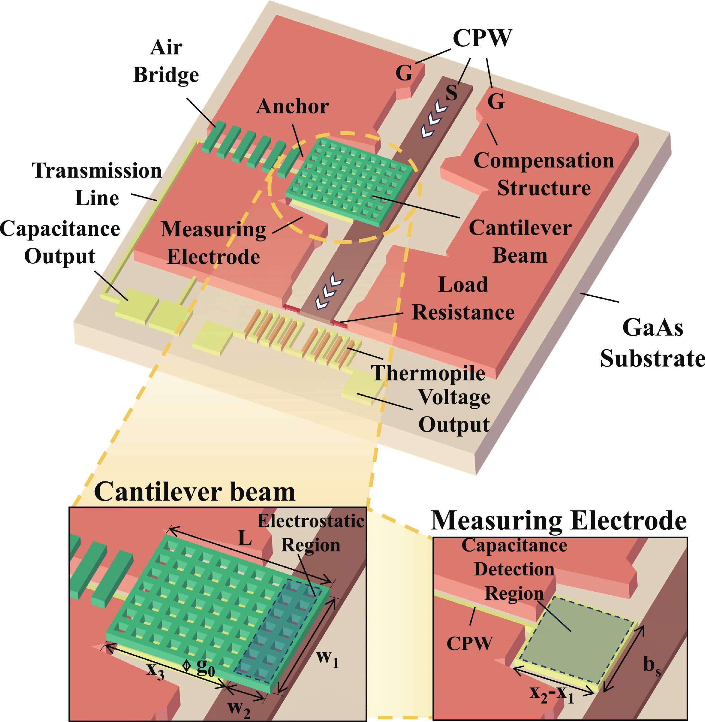
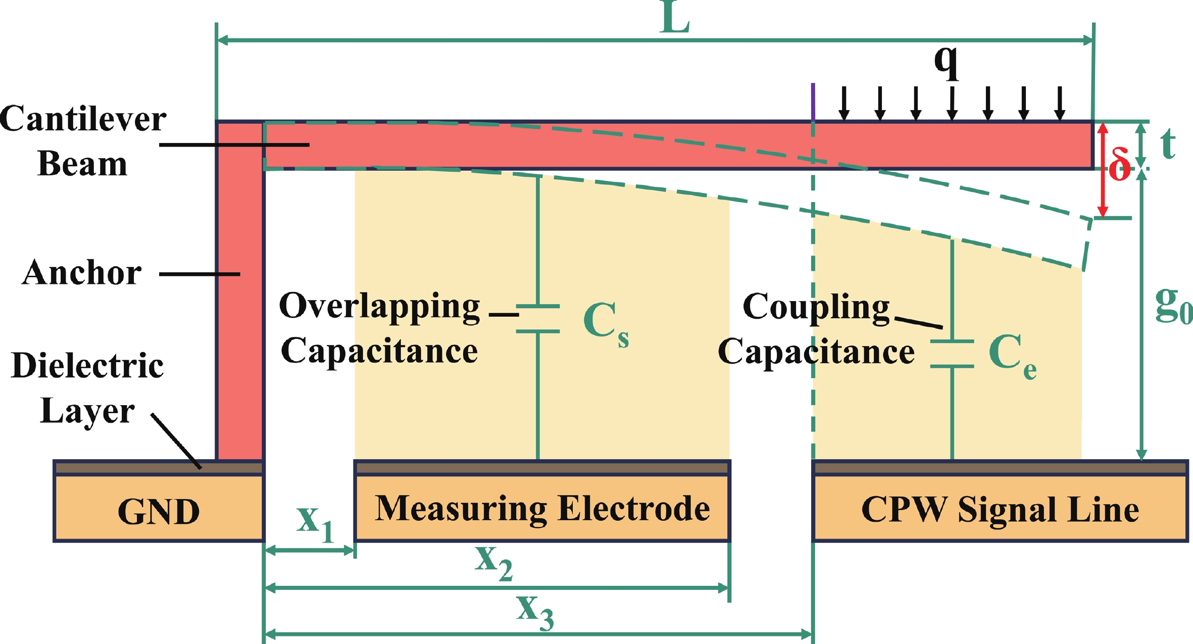
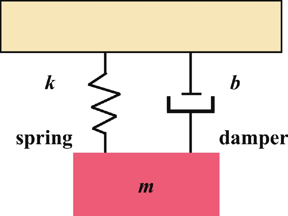
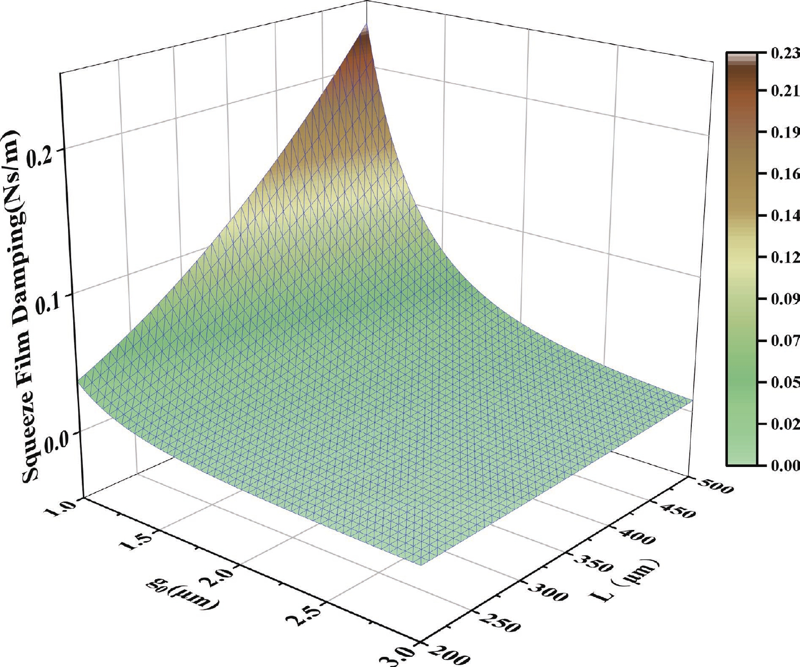
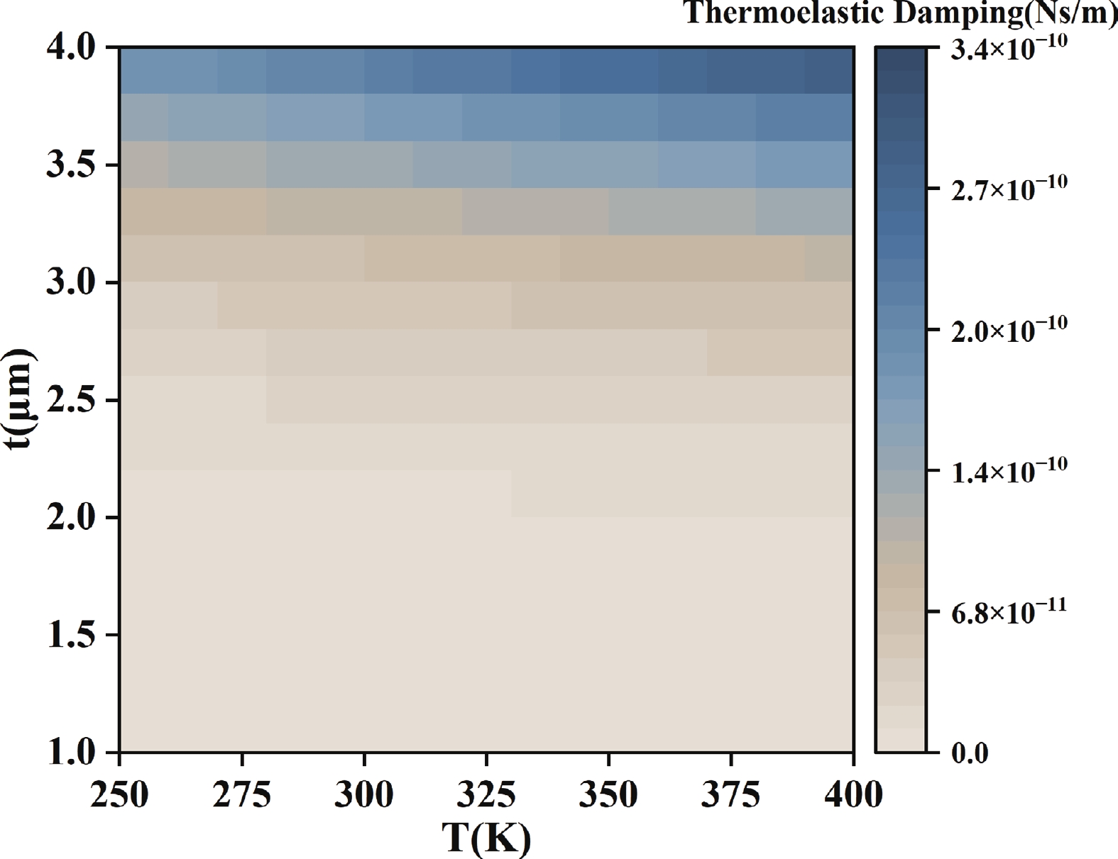
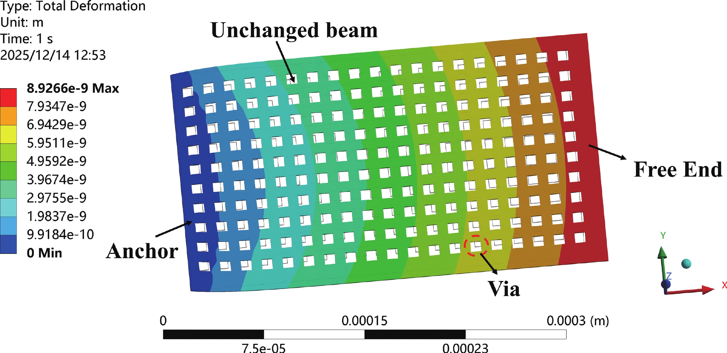
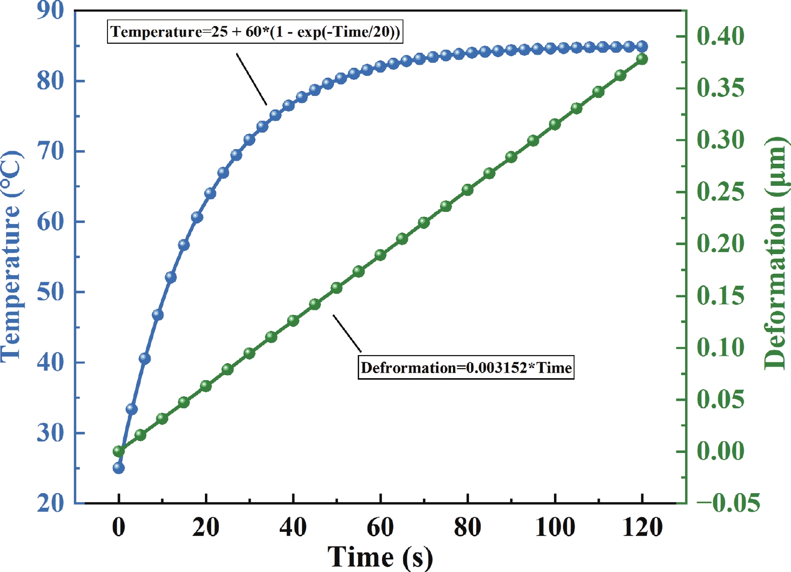
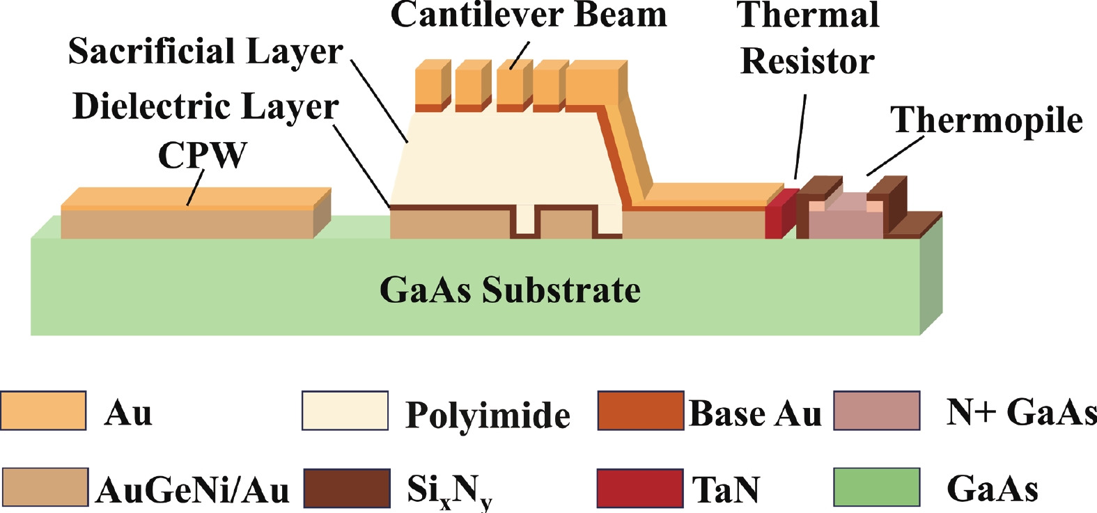
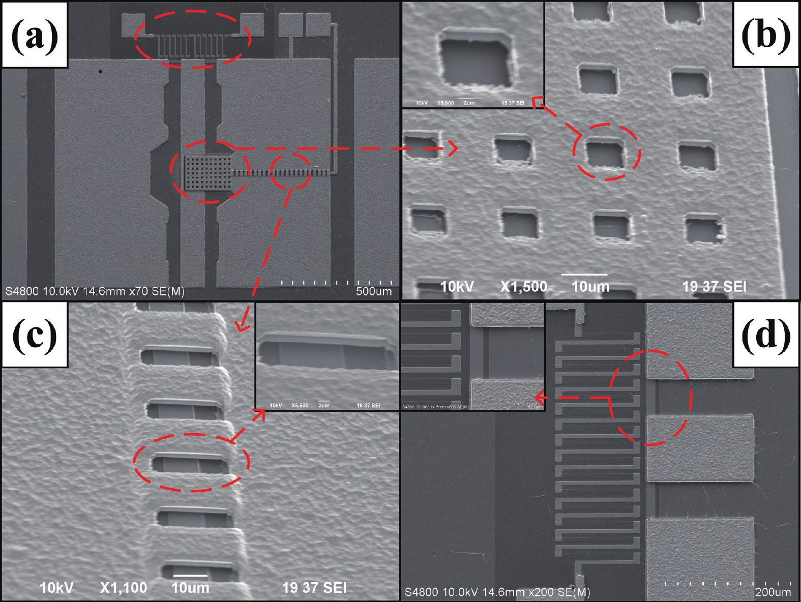
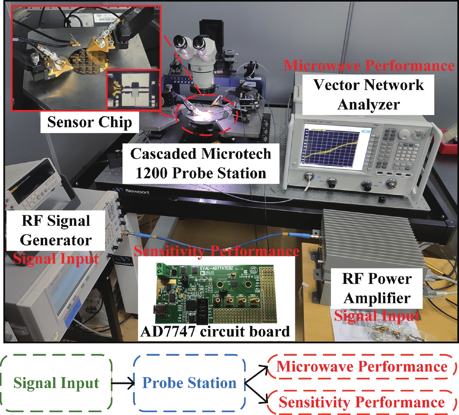
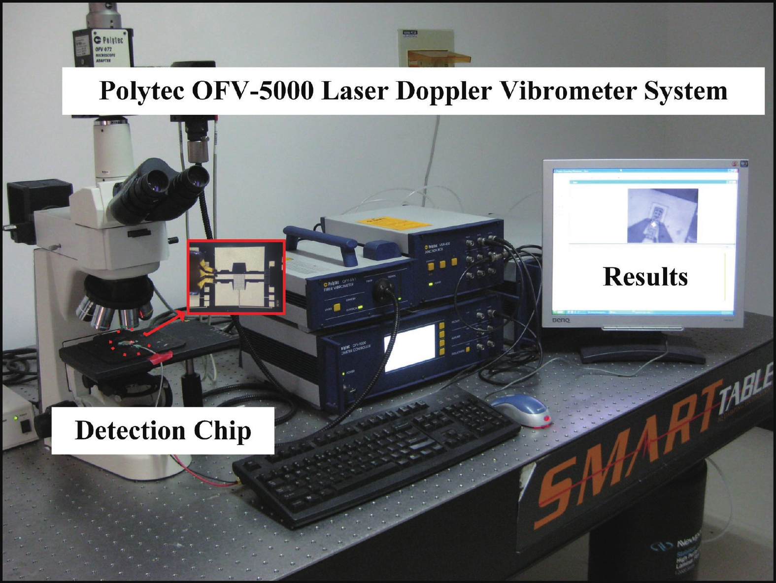
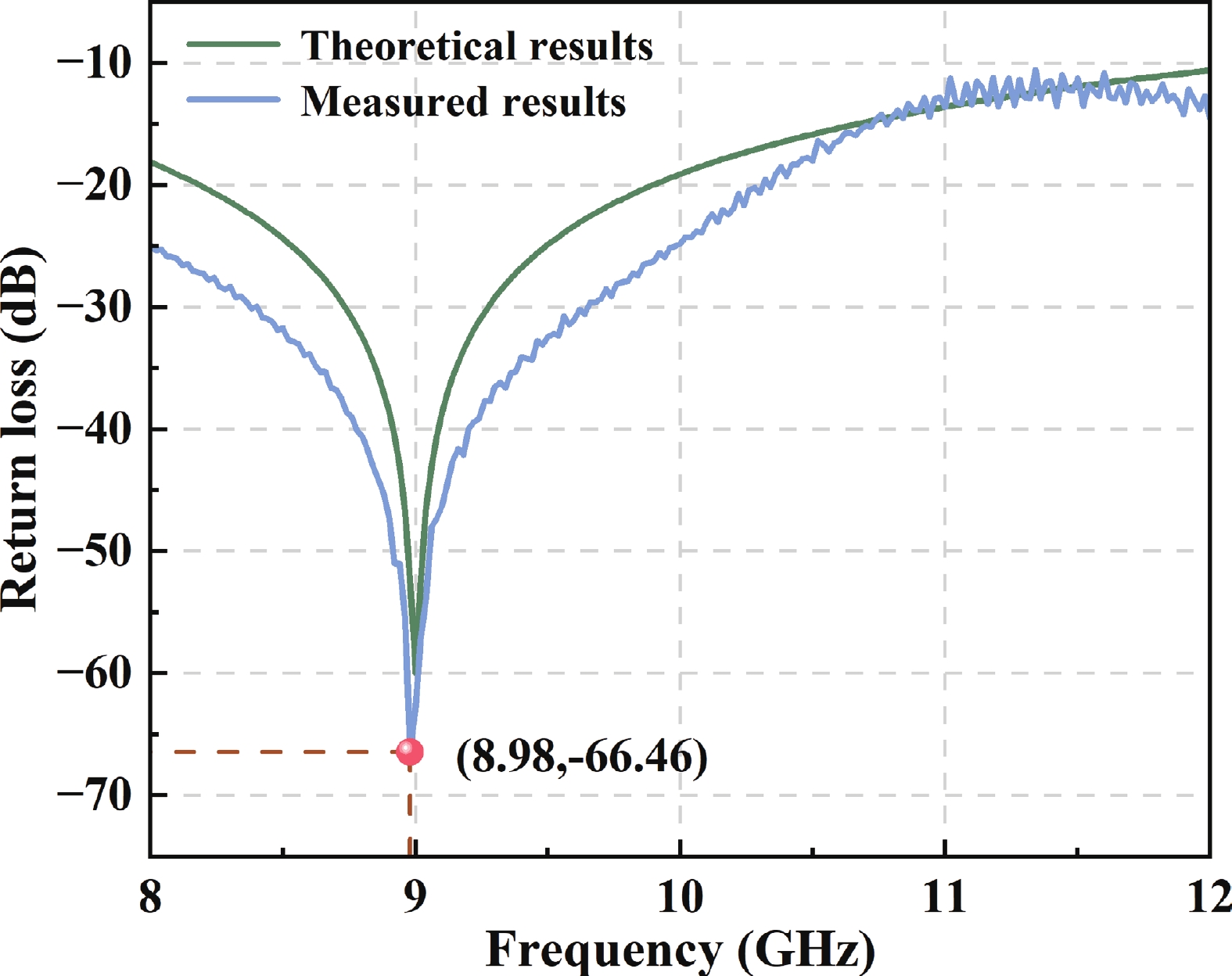
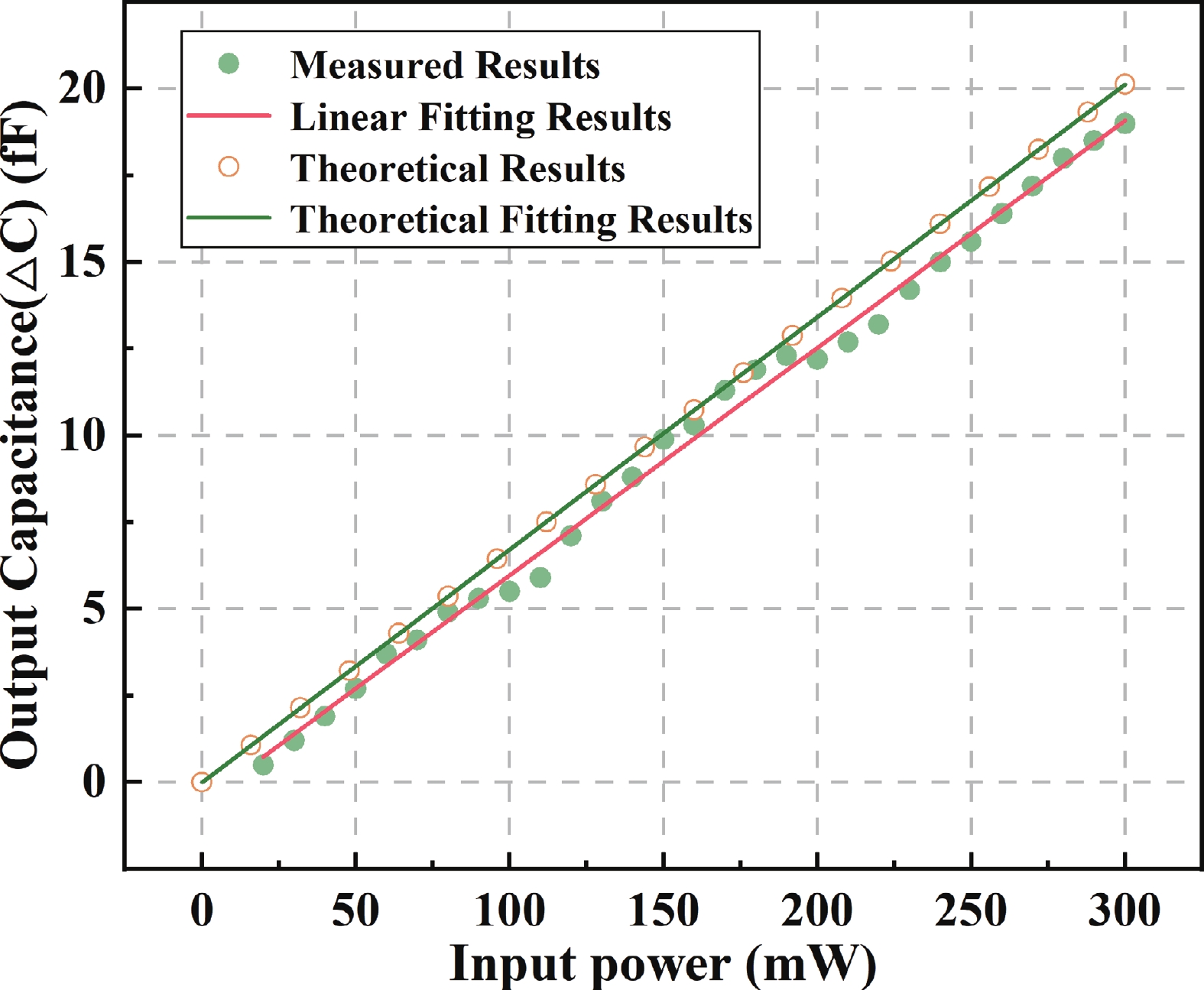
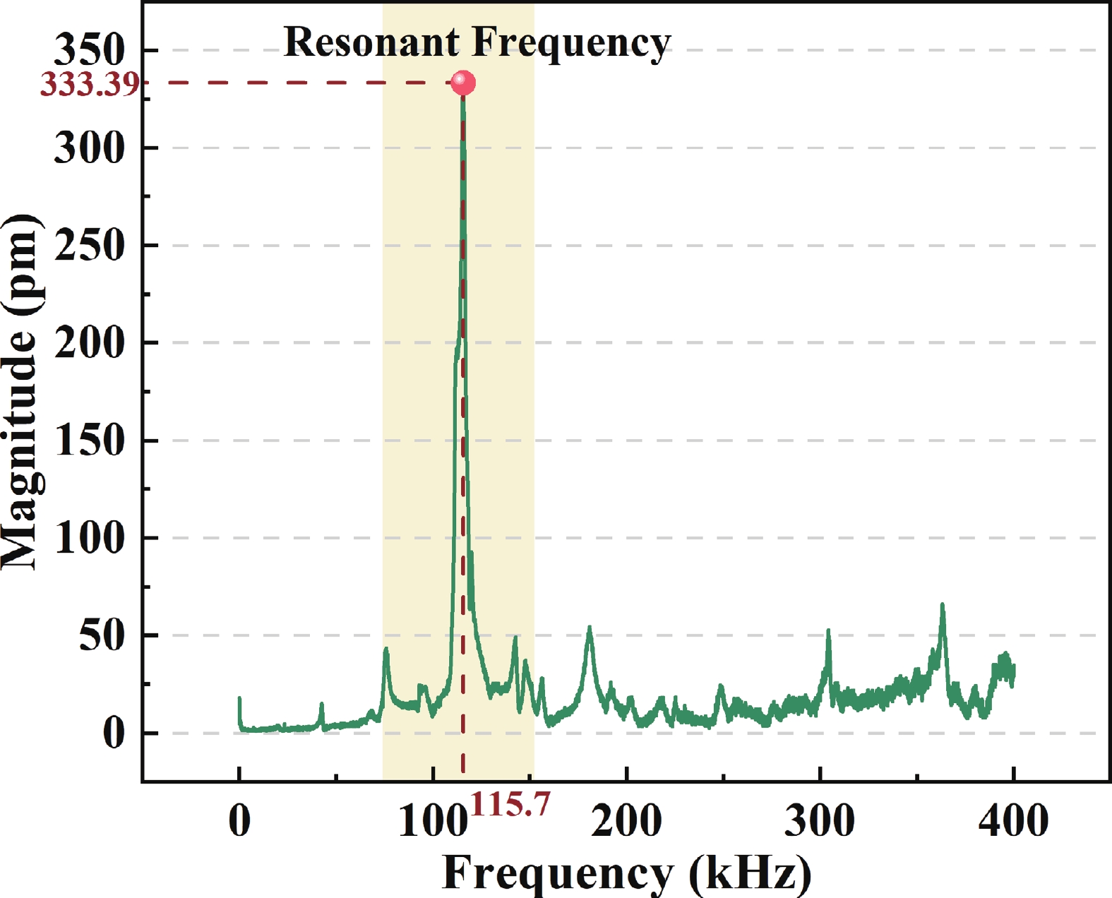
To study MEMS power detection chips more accurately, a thermo-electromechanical coupling model is proposed in this work. The fringing capacitance is included in the model, further refining the expression for the parallel-plate capacitance. Moreover, the squeeze-film damping and thermoelastic damping are considered in the second-order differential equation to study the cantilever vibration. It is found that the squeeze-film damping is the dominant damping of the system, and the cantilever beam exhibits linear expansion with increasing temperature. A dual-channel microwave detection chip is fabricated and measured, and the return loss reaches its minimum of −66.46 dB at 9 GHz, indicating optimal impedance matching at the central frequency. Moreover, the measured sensitivity is approximately 65.6 fF/W. Critically, the measured resonant frequency of the cantilever beam is 115.7 kHz, which is orders of magnitude lower than the input signal frequency. This large separation ensures that the sensor operates in a stable, non-resonant regime, thereby guaranteeing linearity and reliability. These findings demonstrate the excellent microwave performance of the power sensor fabricated in this work, providing valuable insights for optimizing the design of MEMS microwave power detection chips.
J. Semicond.
2026, 47(6): 062401 doi: 10.1088/1674-4926/25120032

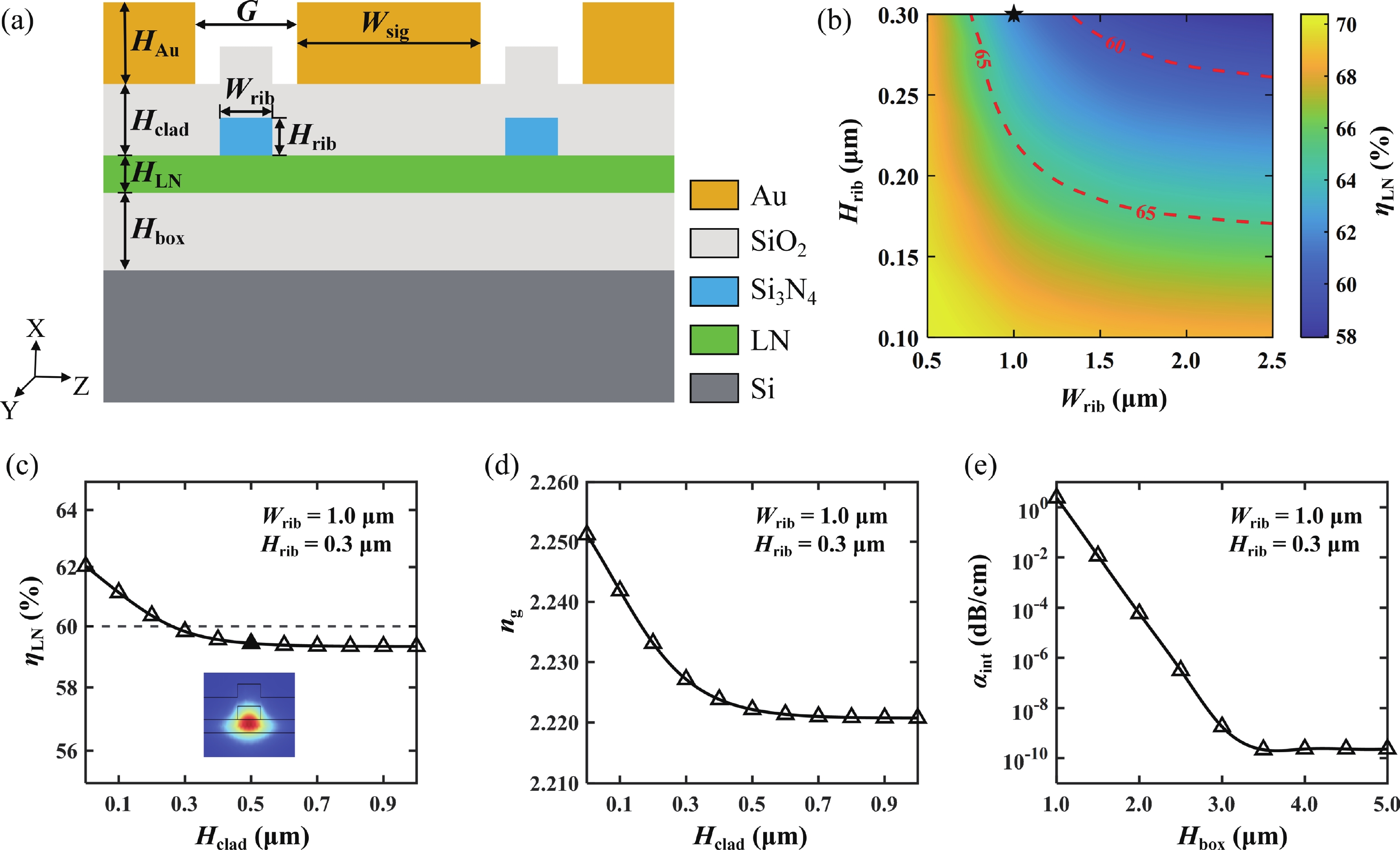
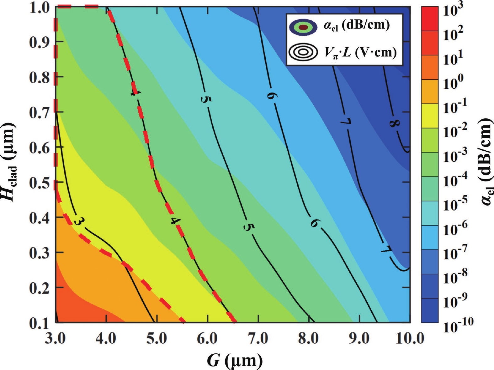
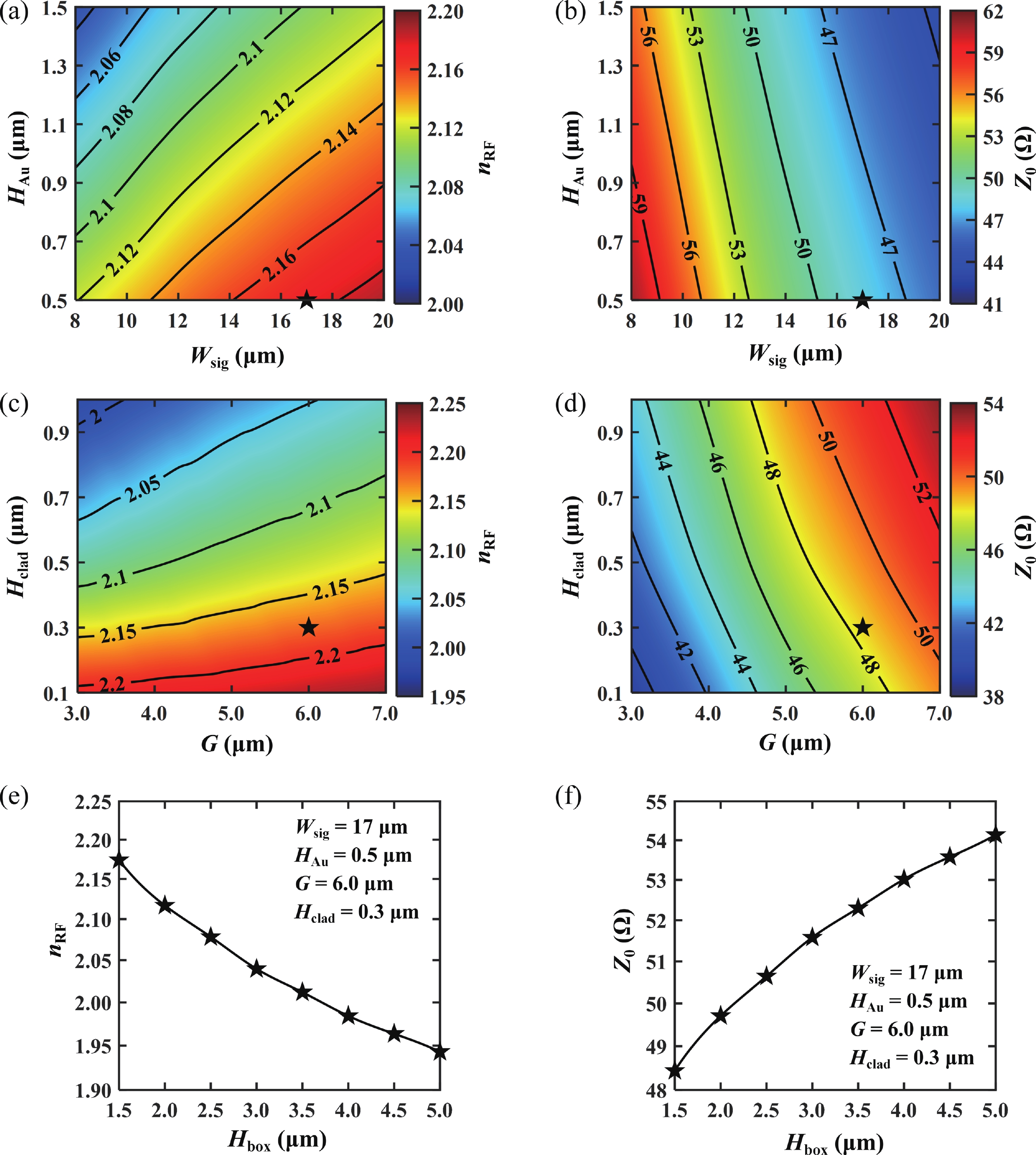
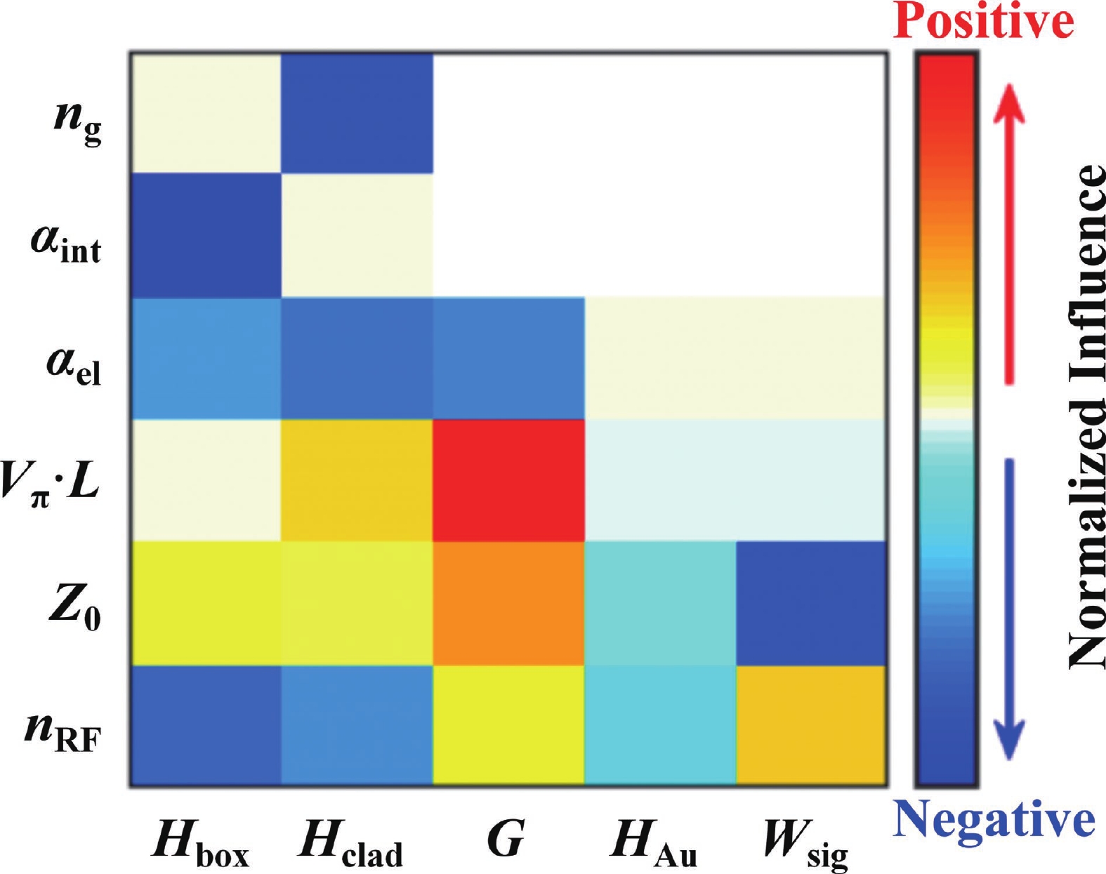
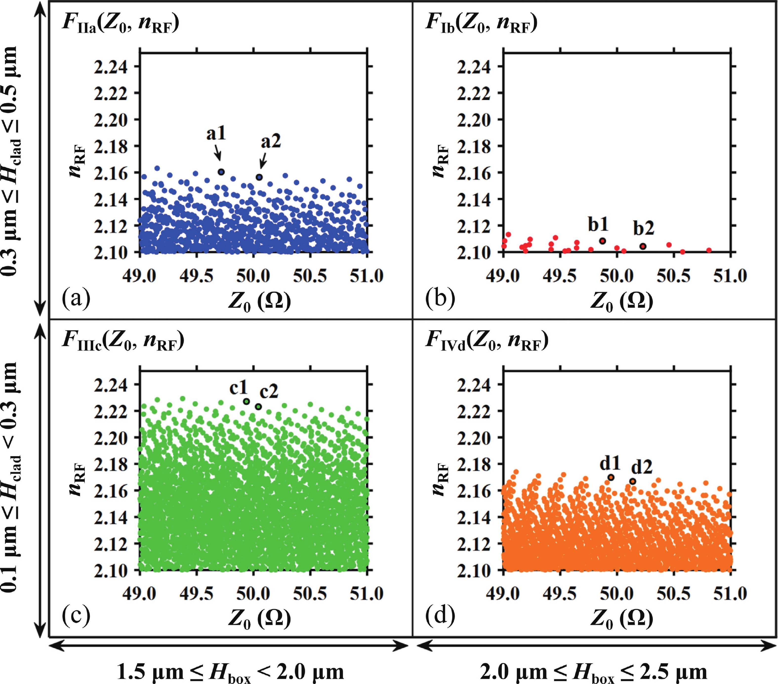
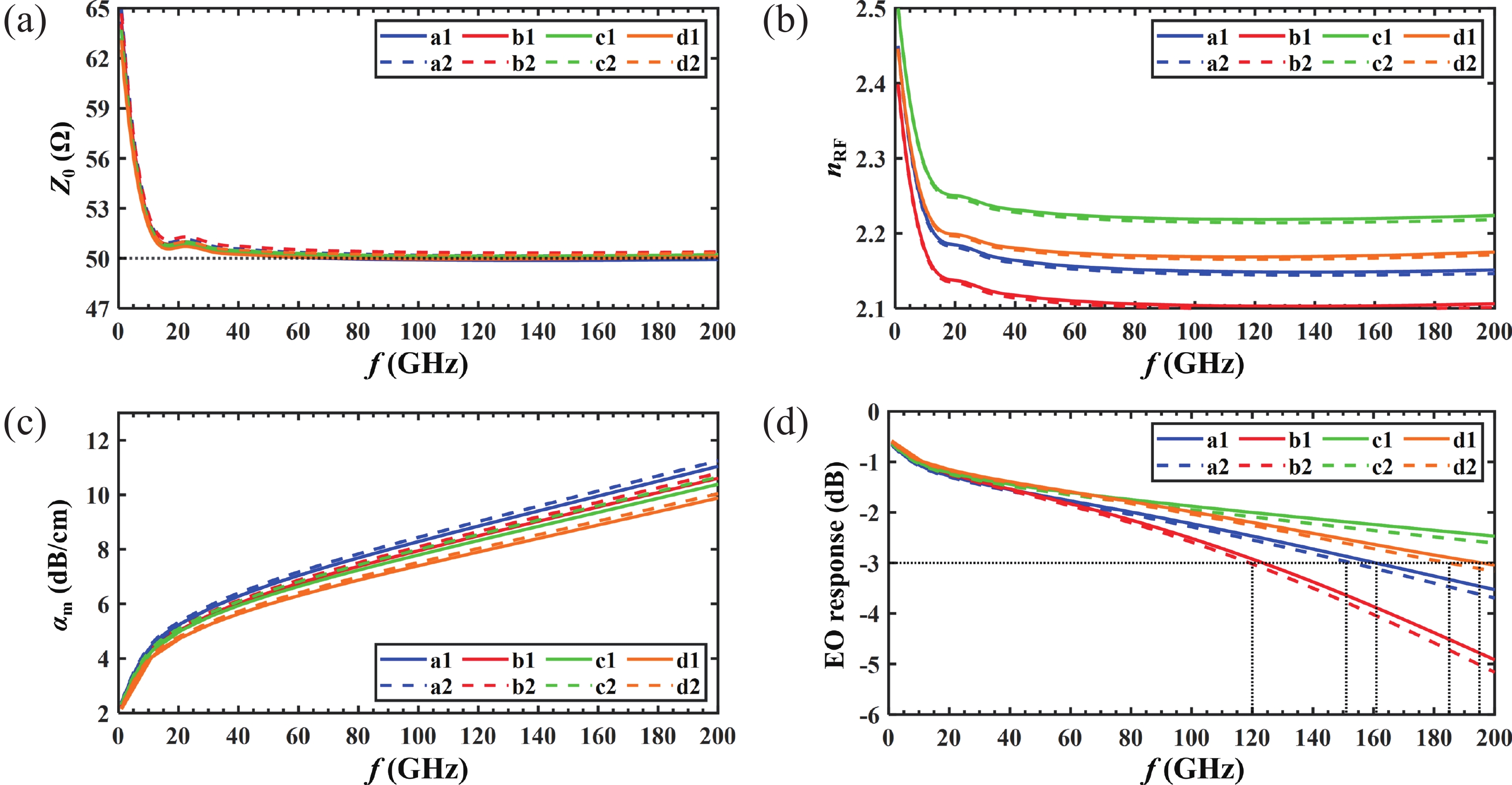
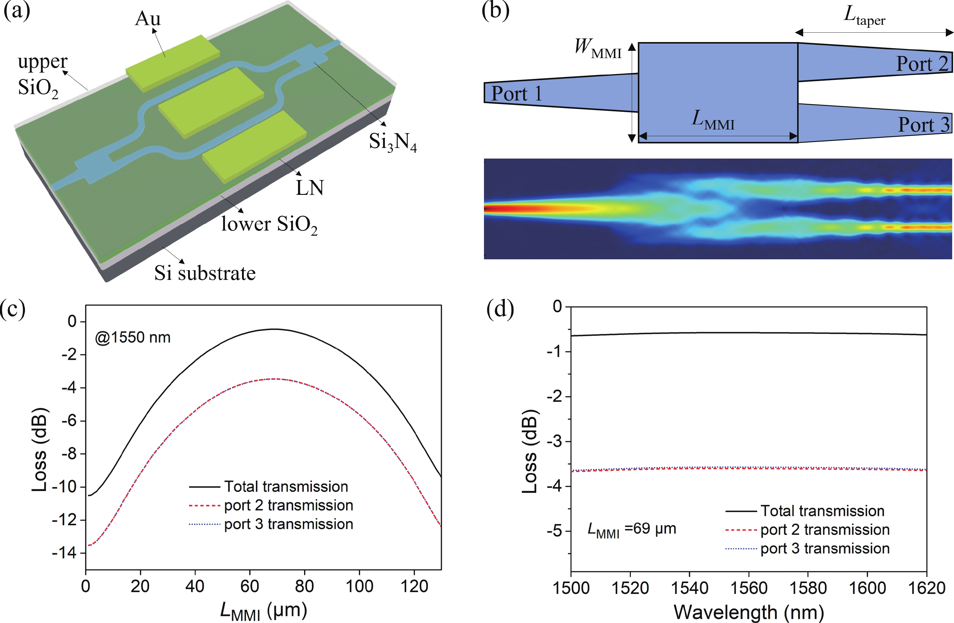
Heterogeneously integrated lithium niobate (LN) electro-optic modulators have great potential for high-speed applications, but challenges remain in optimizing performance, particularly in terms of modulation efficiency, bandwidth, and the trade-offs. This work presents an optimized design for a silicon-nitride (Si3N4)-loaded modulator on a thin-film lithium niobate (TFLN) platform, consisting of 300 nm-thick LN film and 300 nm-thick Si3N4 optical waveguide. By systematically optimizing the dielectric layer thickness, electrode parameters, and achieving velocity and impedance matching, we demonstrate a modulator with a bandwidth exceeding 200 GHz. Our collaborative optimization scheme highlights the critical role of reducing the silicon oxide box layer thickness for velocity matching. We show that multiple structural configurations can achieve bandwidths greater than 120 GHz with Vπ·L< 4 V·cm, providing feasibility in low-loss design and fabrication. These findings offer valuable design guidelines for high-performance electro-optic modulators suitable for data communications.
J. Semicond.
2026, 47(6): 062501 doi: 10.1088/1674-4926/25090027
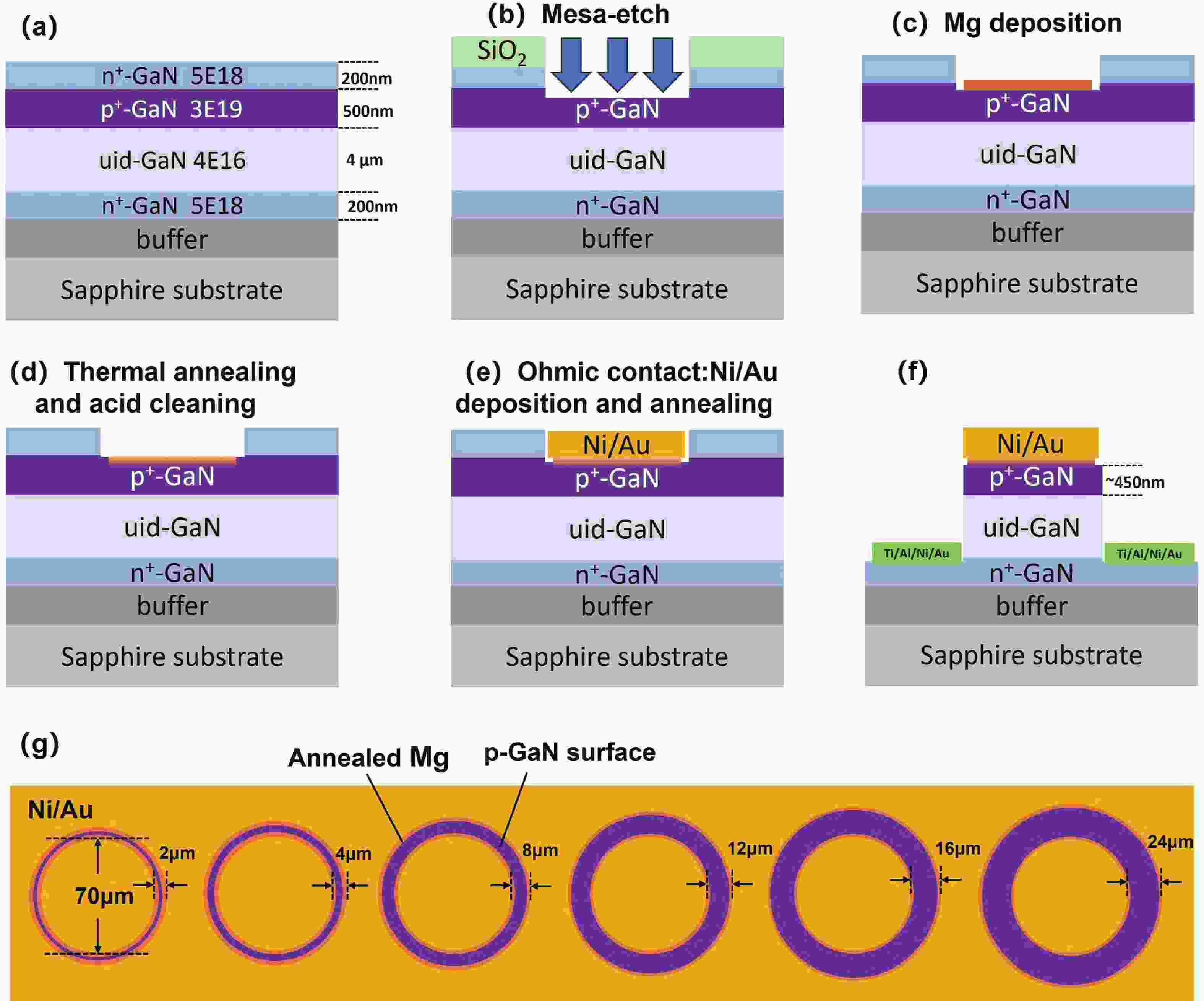
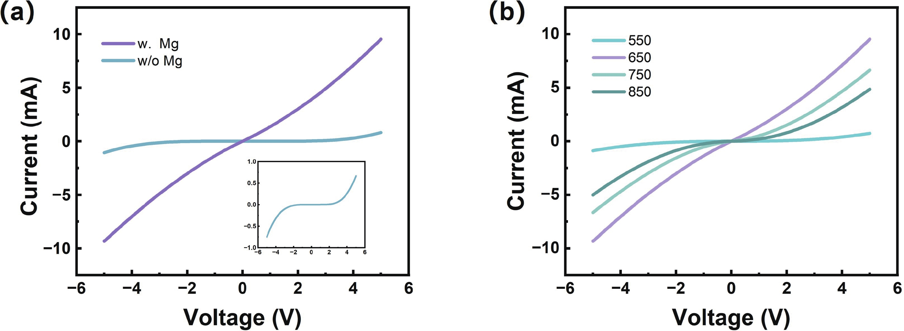
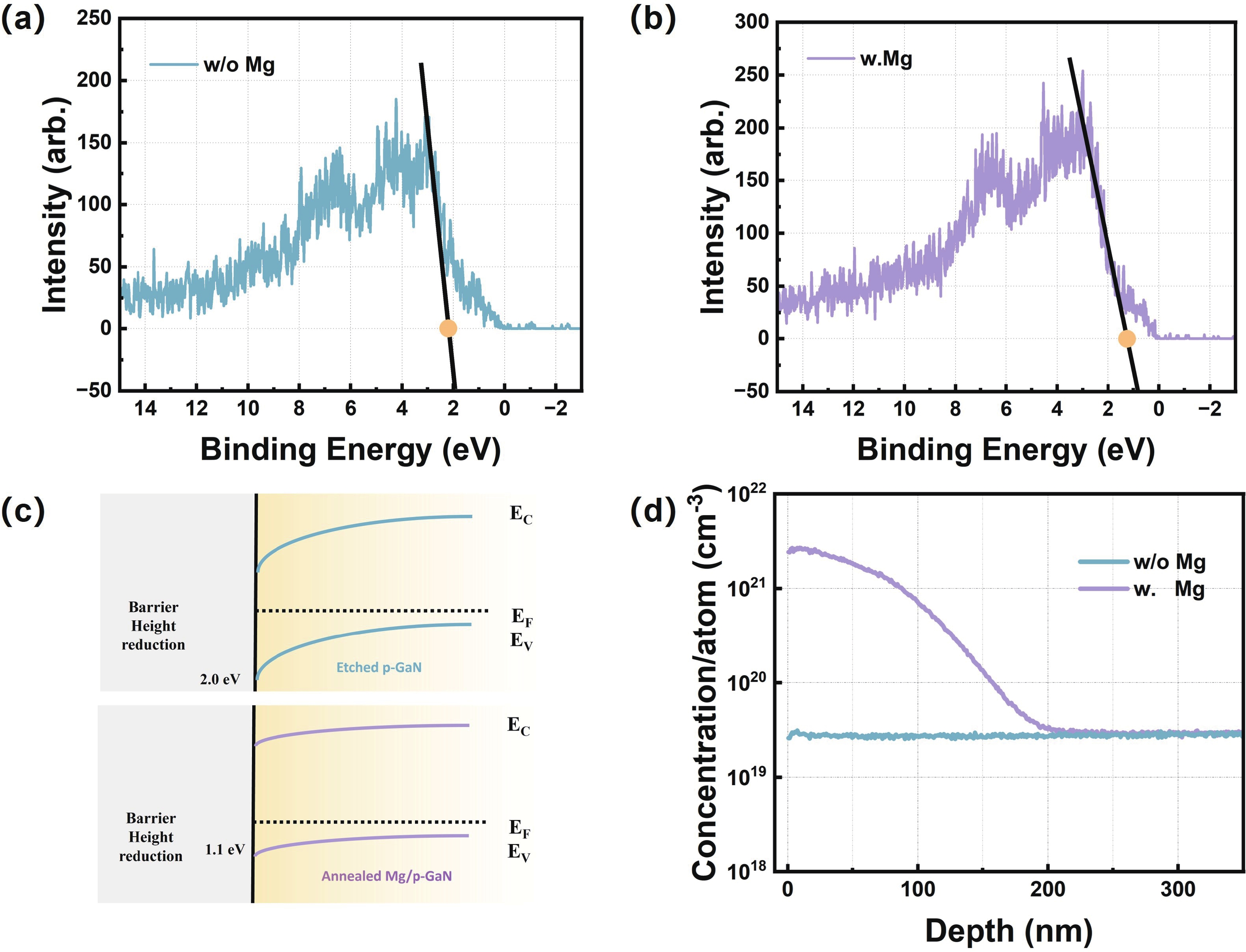
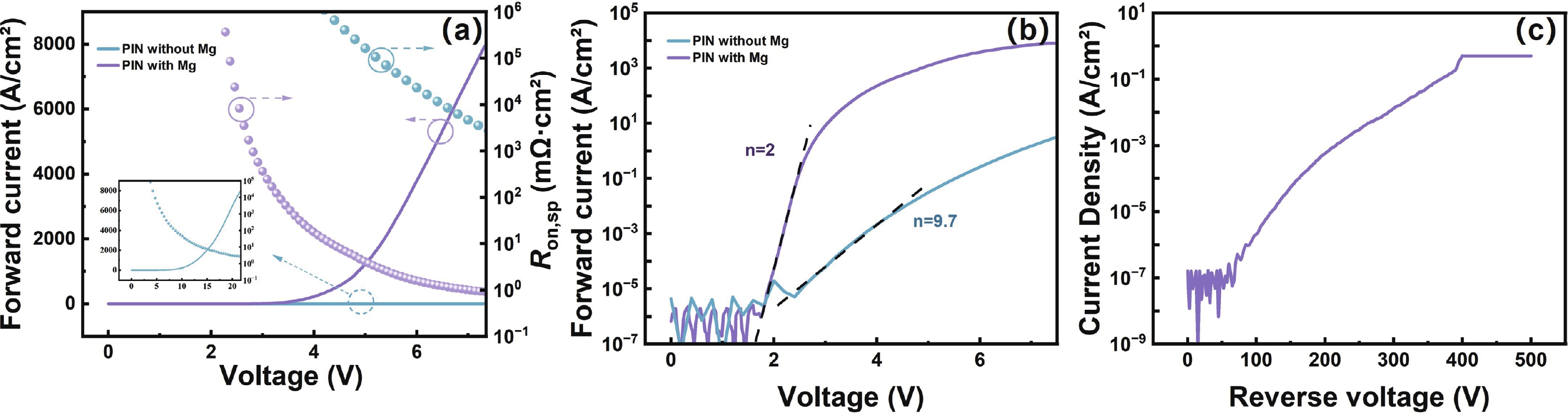
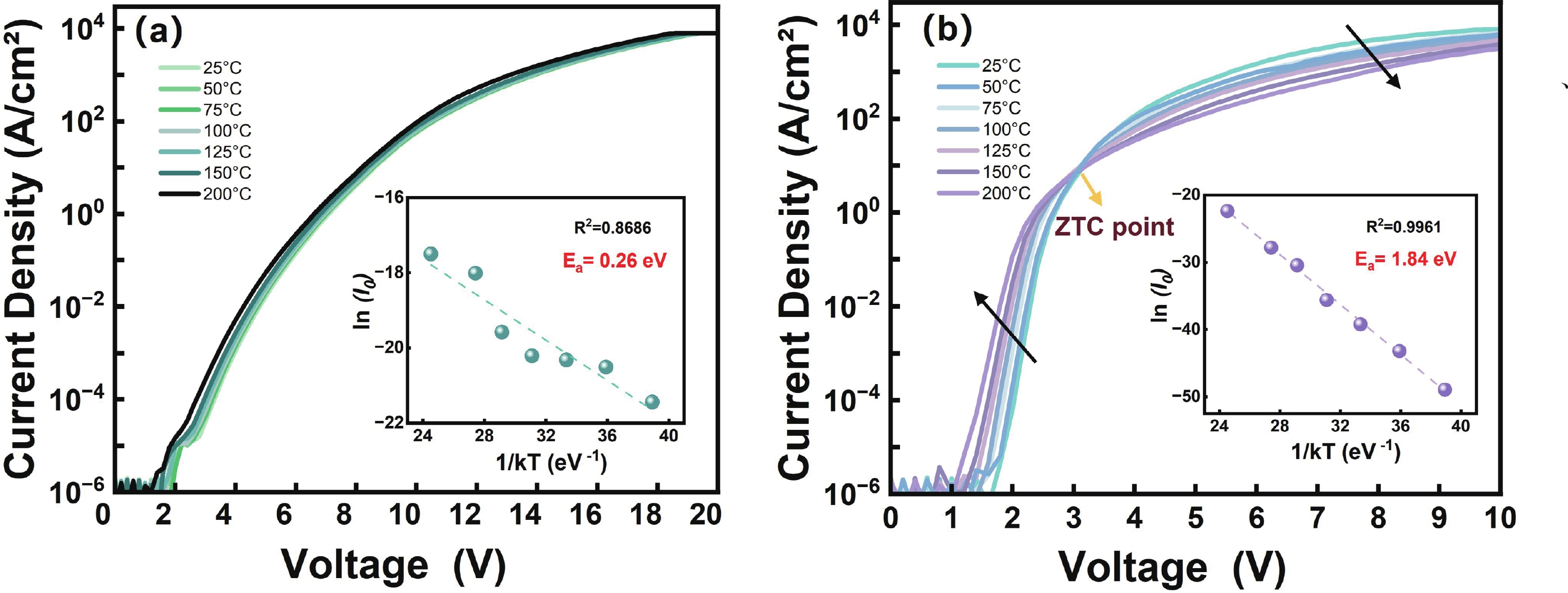
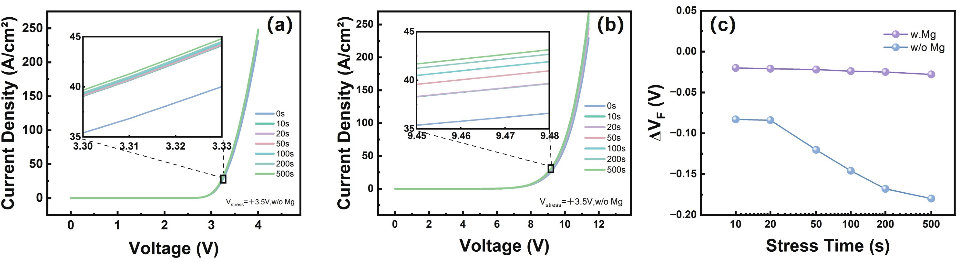
This work demonstrates a high-performance vertical GaN p−i−n diode based on a buried p-layer n-p−i−n epitaxial structure. The post-etch magnesium (Mg) diffusion process is applied to suppress the etch-induced surface damage on the p-GaN layer. The Mg diffusion effectively reduces the valence band barrier from 2 to 1.1 eV, yielding a low specific contact resistivity of 6.521 × 10⁻⁴ Ω·cm2. As a result, the fabricated devices exhibit markedly enhanced forward characteristics, including a reduced turn-on voltage of 3.3 V and a specific on-resistance of 0.92 mΩ·cm2. Temperature-dependent forward I−V measurements indicate that the dominant carrier transport mechanism evolves from defect-related tunneling in the etched devices toward transport dominated by intrinsic p–n junction conduction after Mg diffusion. In addition, the devices exhibit excellent stability in forward conduction, with a voltage variation of approximately 0.028 V. These results indicate that Mg diffusion effectively improves the contact characteristics degraded by ICP etching and provide a viable approach for achieving high-performance and reliable vertical GaN power devices.
J. Semicond.
2026, 47(6): 062502 doi: 10.1088/1674-4926/25120047
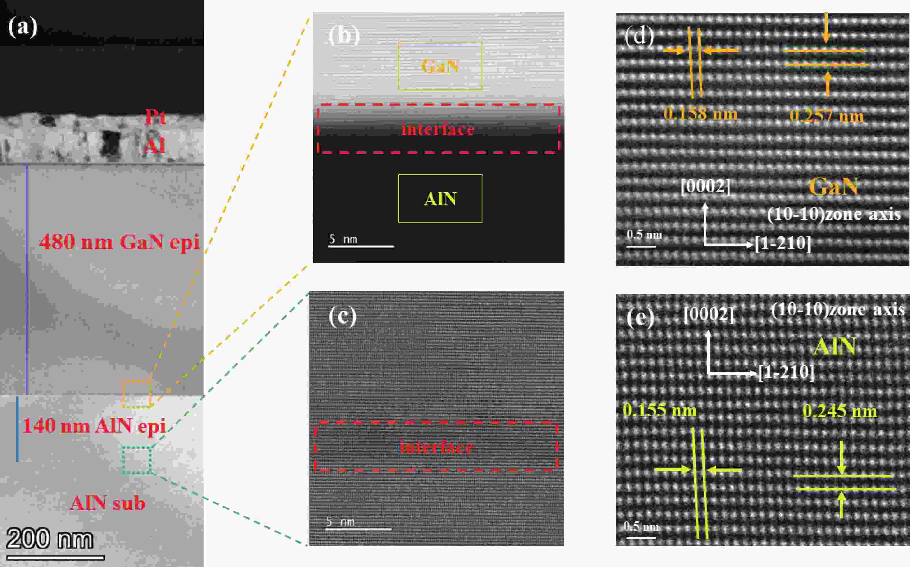
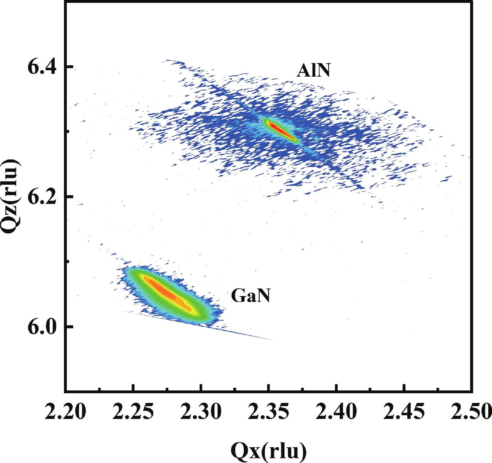
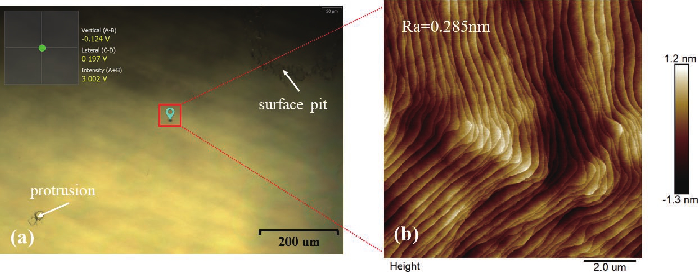
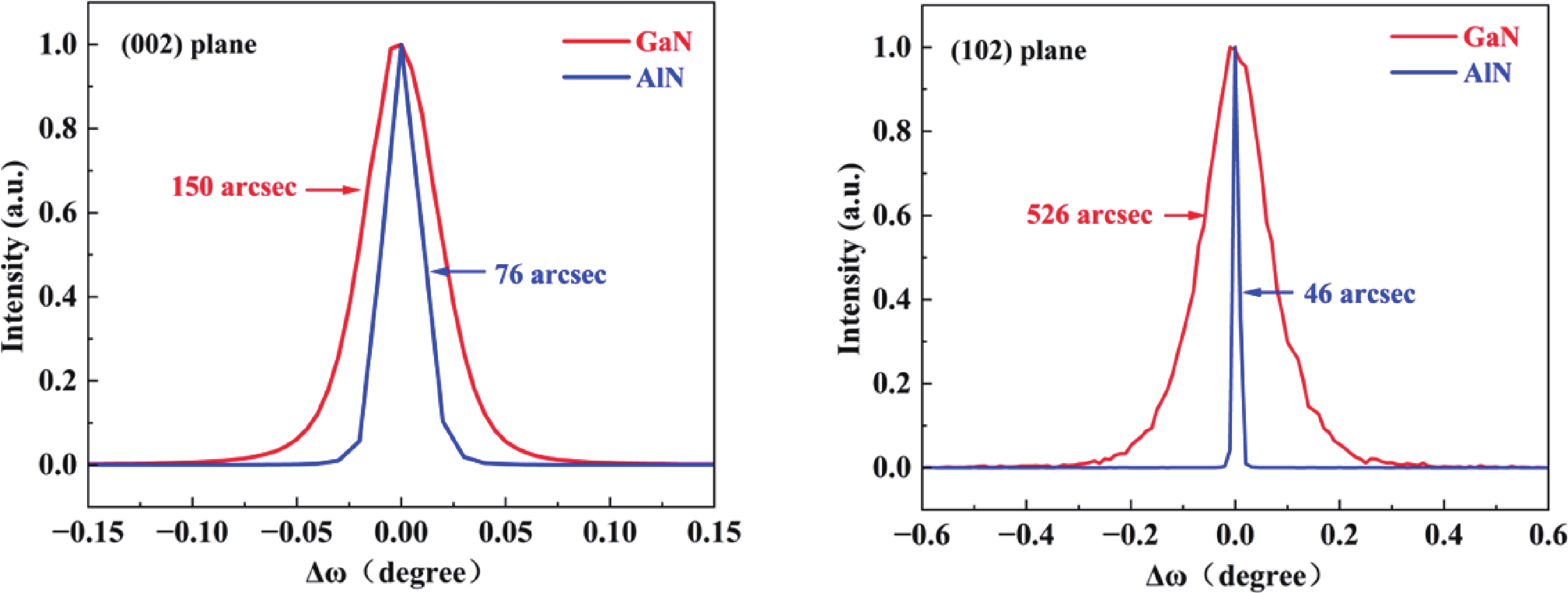
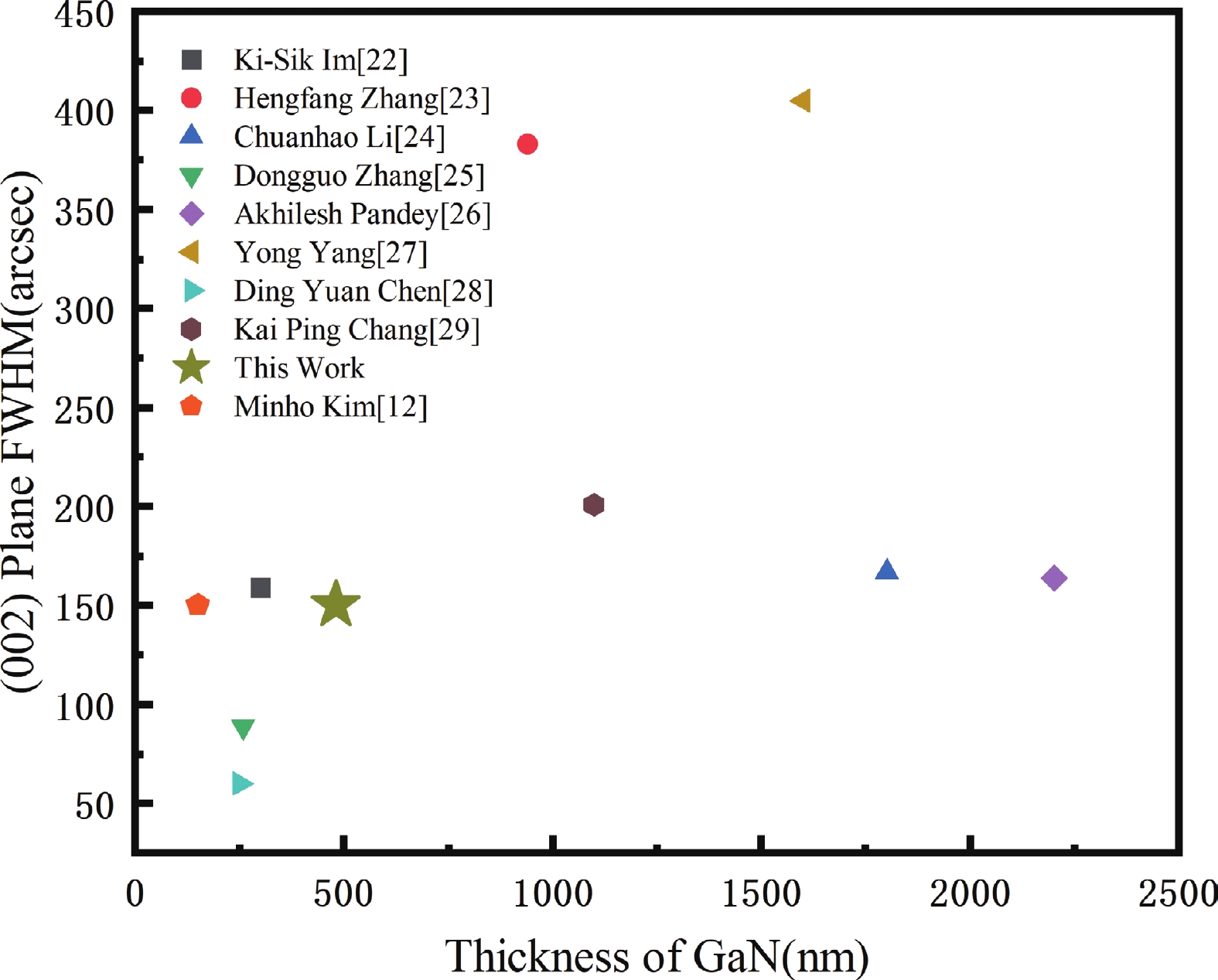
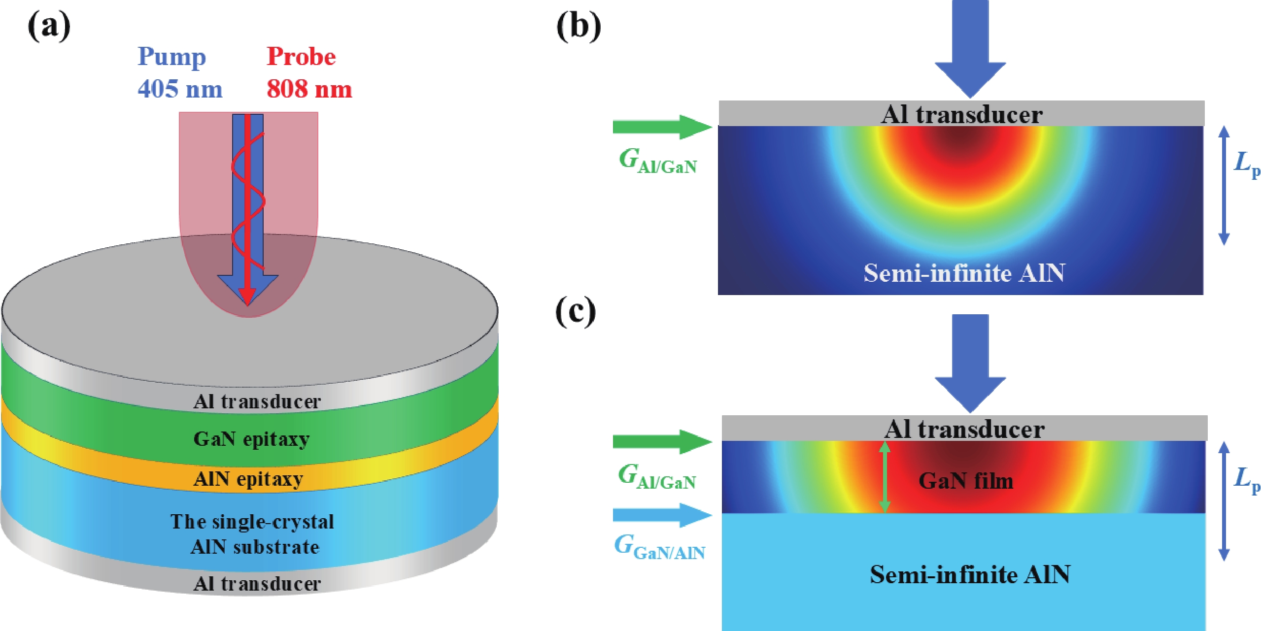
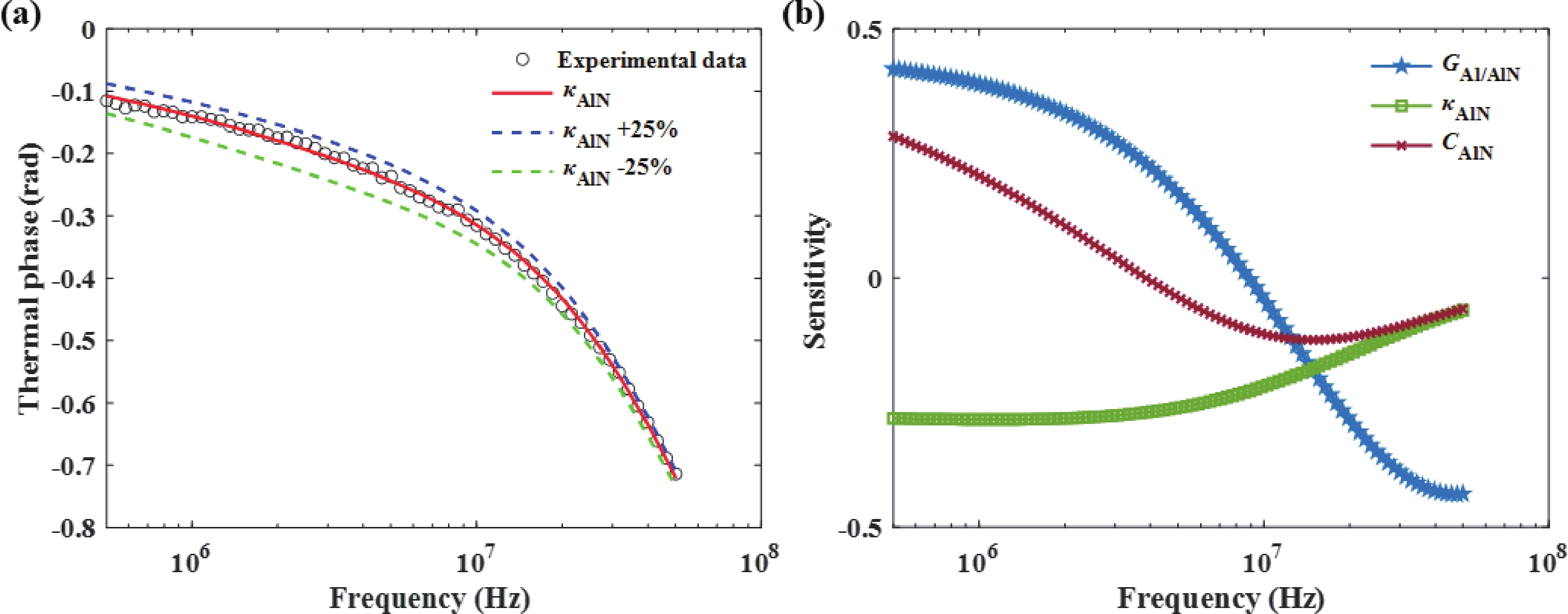
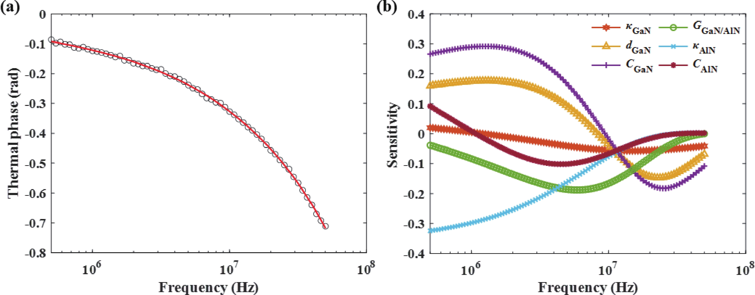
Bulk single-crystal aluminum nitride (BSC AlN) substrates are known to be ideal platforms for constructing high-power and DUV optoelectronic nitride devices. However, high-quality epitaxial growth of nitride films on BSC AlN and related characterization is still far from being well studied. The challenges and uncertainties in doing accurate thermal characterization on such heterostructures are not fully recognized. In this study, we successfully fabricated a buffer-free thin GaN/AlN heterostructure on a BSC AlN substrate via metal−organic chemical vapor deposition (MOCVD) technology. This heterostructure consists of a 140 nm-thick AlN homoepitaxial layer and a 480 nm-thick GaN epitaxial layer. Characterization results indicate that the prepared heterojunction has excellent crystal quality and smooth surface morphology. To accurately obtain the thermophysical parameters of the heterostructure, this study employed broadband frequency domain thermoreflectance (BB-FDTR) technology, and careful measurements with detailed data analysis were demonstrated. In addition to showing the feasibility of epitaxial growth of high-quality thin film GaN directly on BSC AlN substrates, this study also provides key experimental data for evaluating the heat dissipation advantages of GaN/AlN heterostructures.
J. Semicond.
2026, 47(6): 062701 doi: 10.1088/1674-4926/25120039
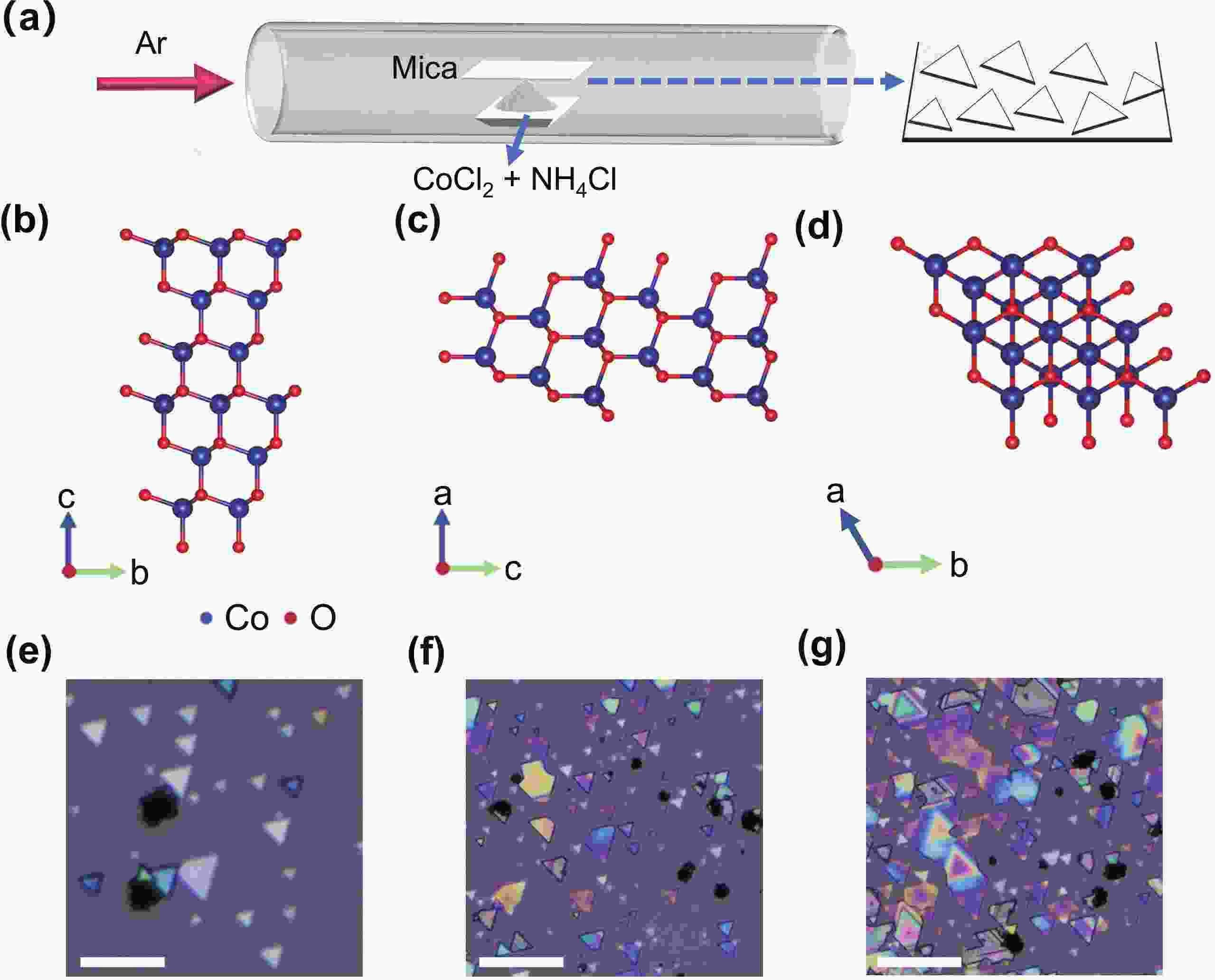
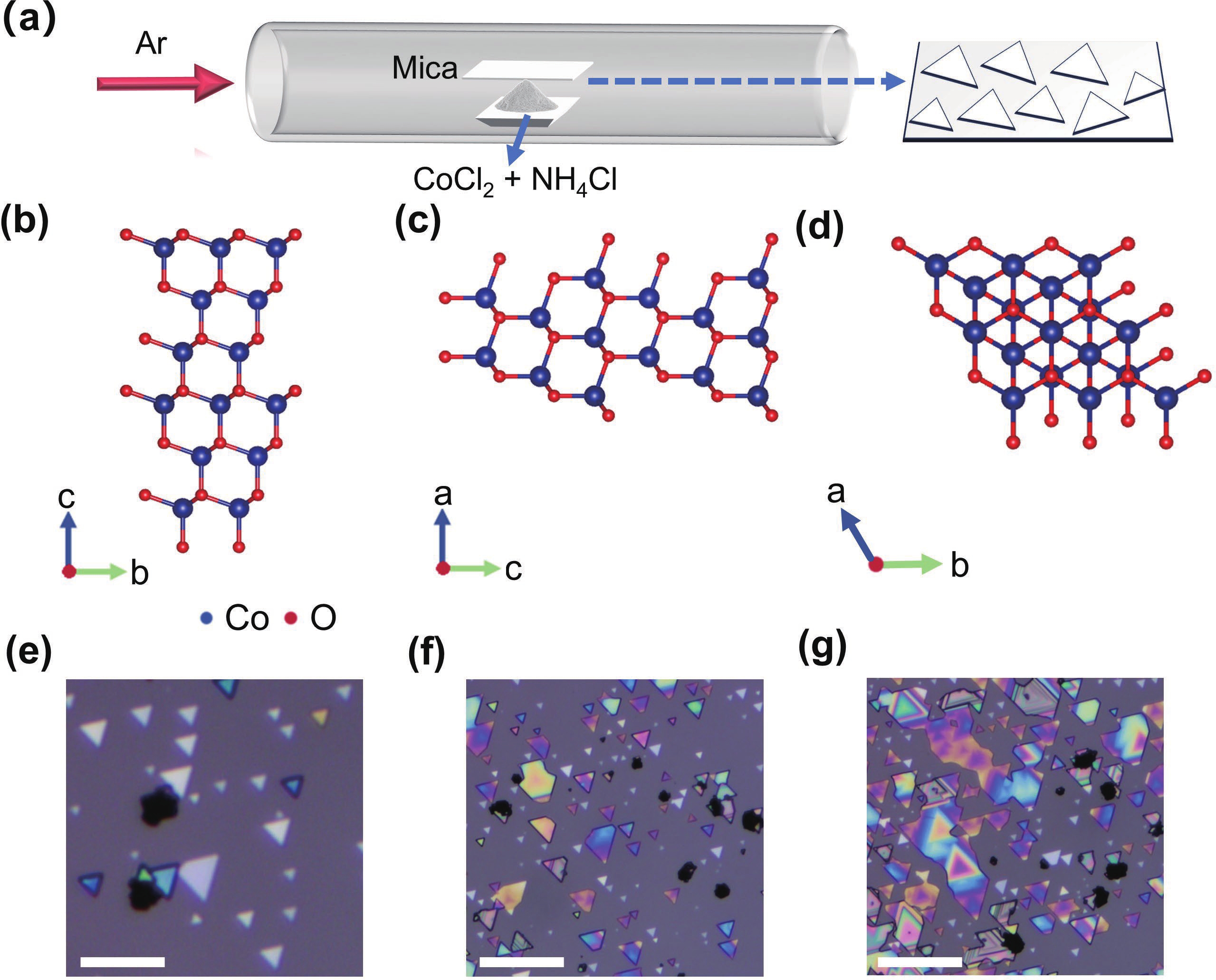
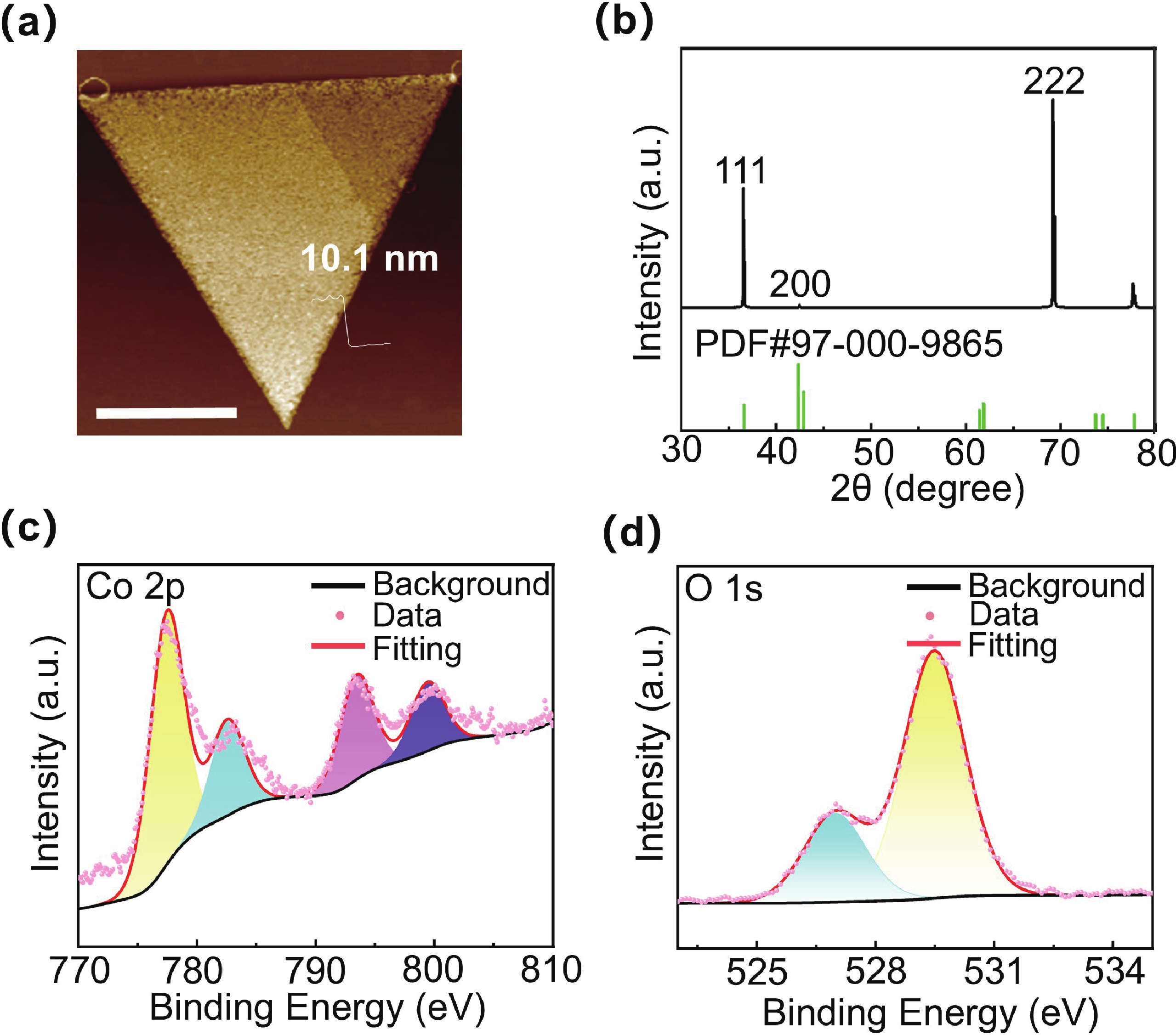
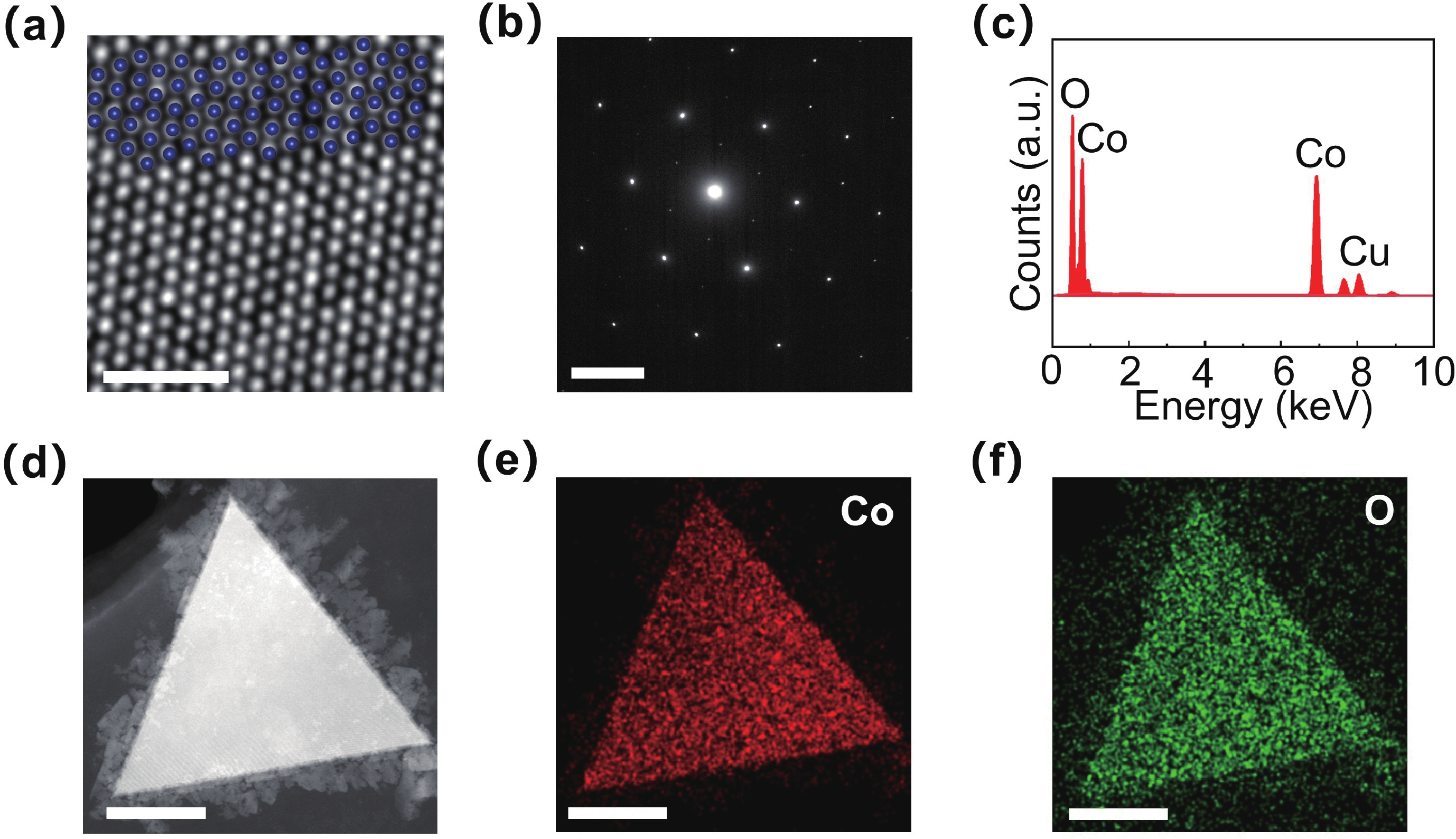
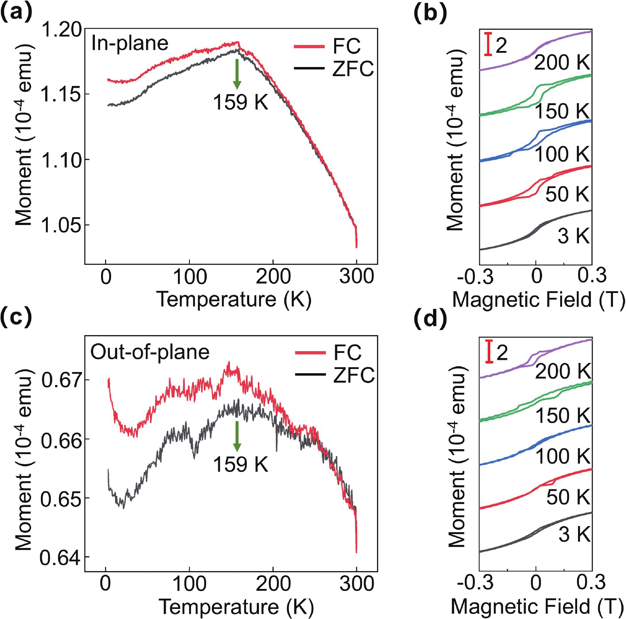
Two-dimensional (2D) magnetic materials have attracted significant attention owing to their tunable magnetic properties and prospective applications in next-generation spintronic devices. However, their practical utilization is often limited by poor air stability. 2D magnetic metal oxides, which generally exhibit better stability under ambient conditions, represent a promising alternative. In this work, high-quality CoO nanosheets were successfully synthesized via chemical vapor deposition. Structural characterization confirms a well-defined triangular morphology and single-crystalline nature, with the thinnest nanosheets reaching approximately 10.1 nm in thickness. Magnetic measurements reveal significant magnetic anisotropy with an in-plane easy magnetization axis and a transition temperature of approximately 159 K. Our study provides a feasible approach for the controllable synthesis of air-stable 2D magnetic semiconductors, thereby laying a foundation for their potential application in low-power spintronic devices.
J. Semicond.
2026, 47(6): 062702 doi: 10.1088/1674-4926/26010036
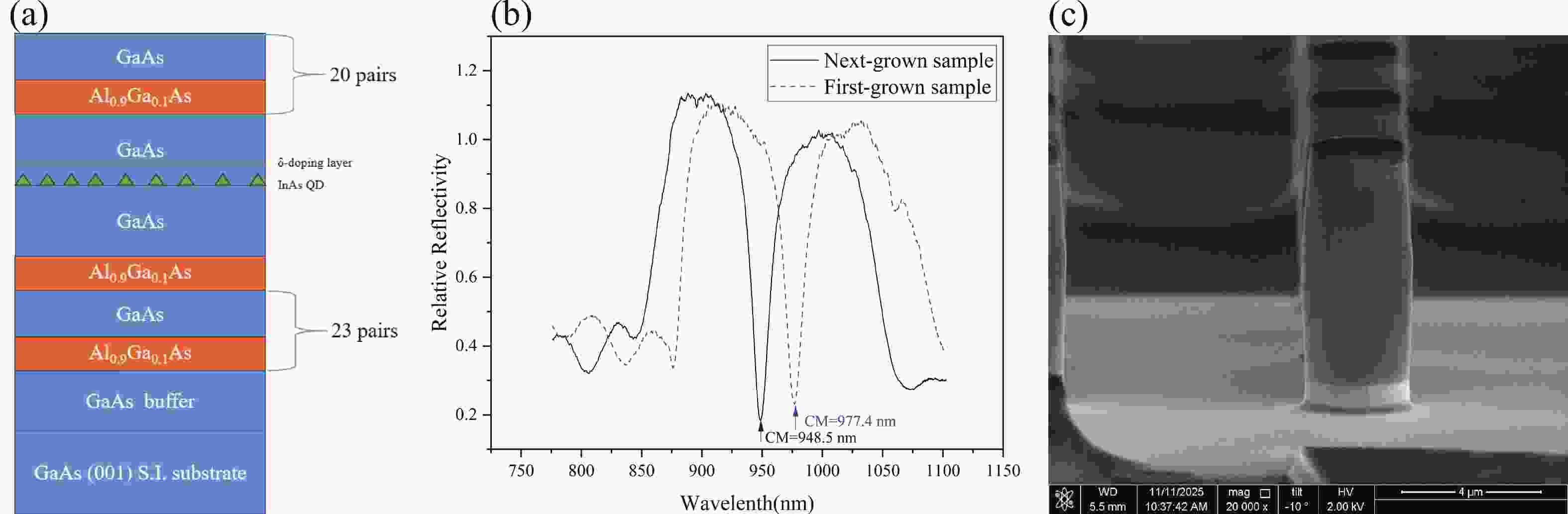
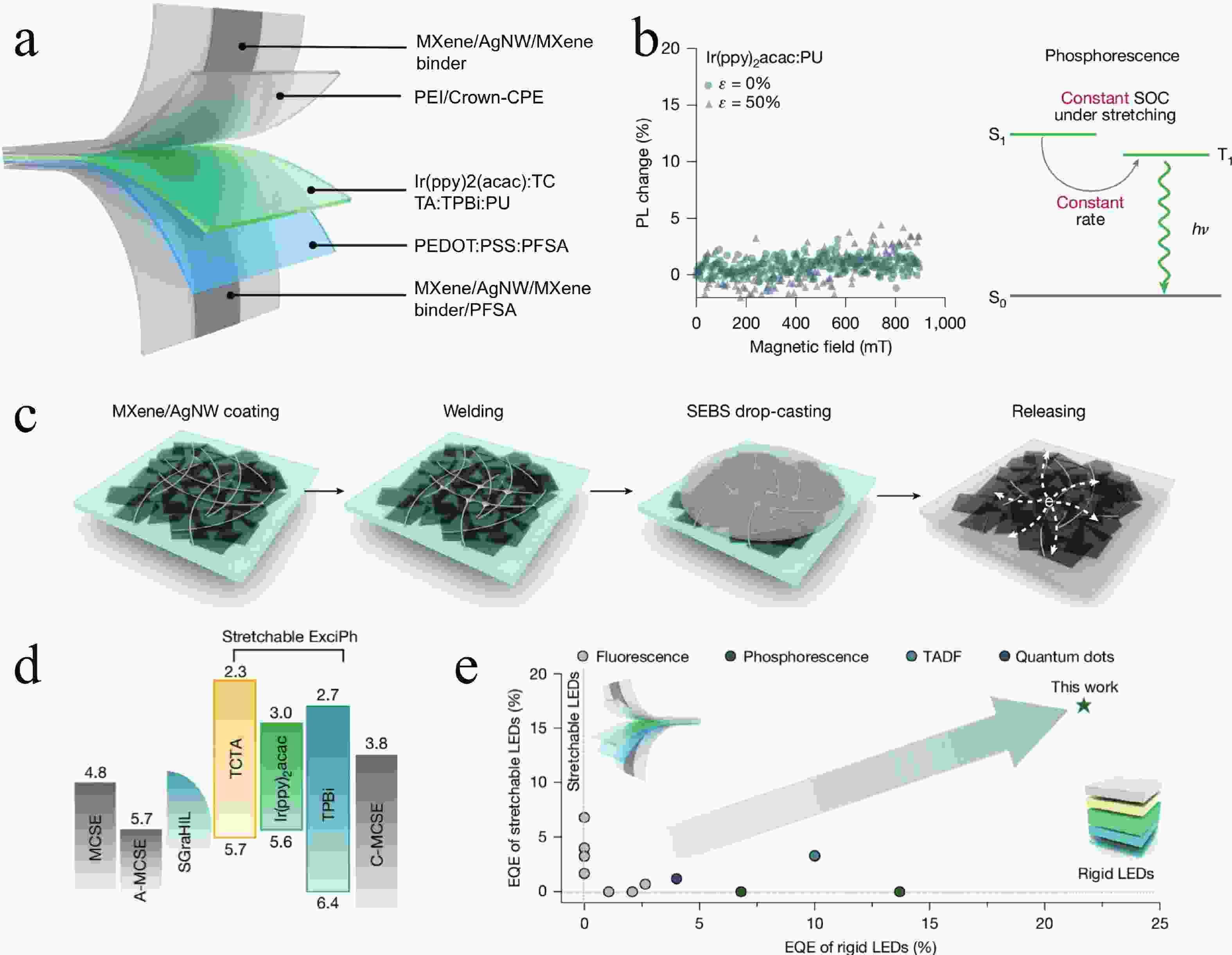
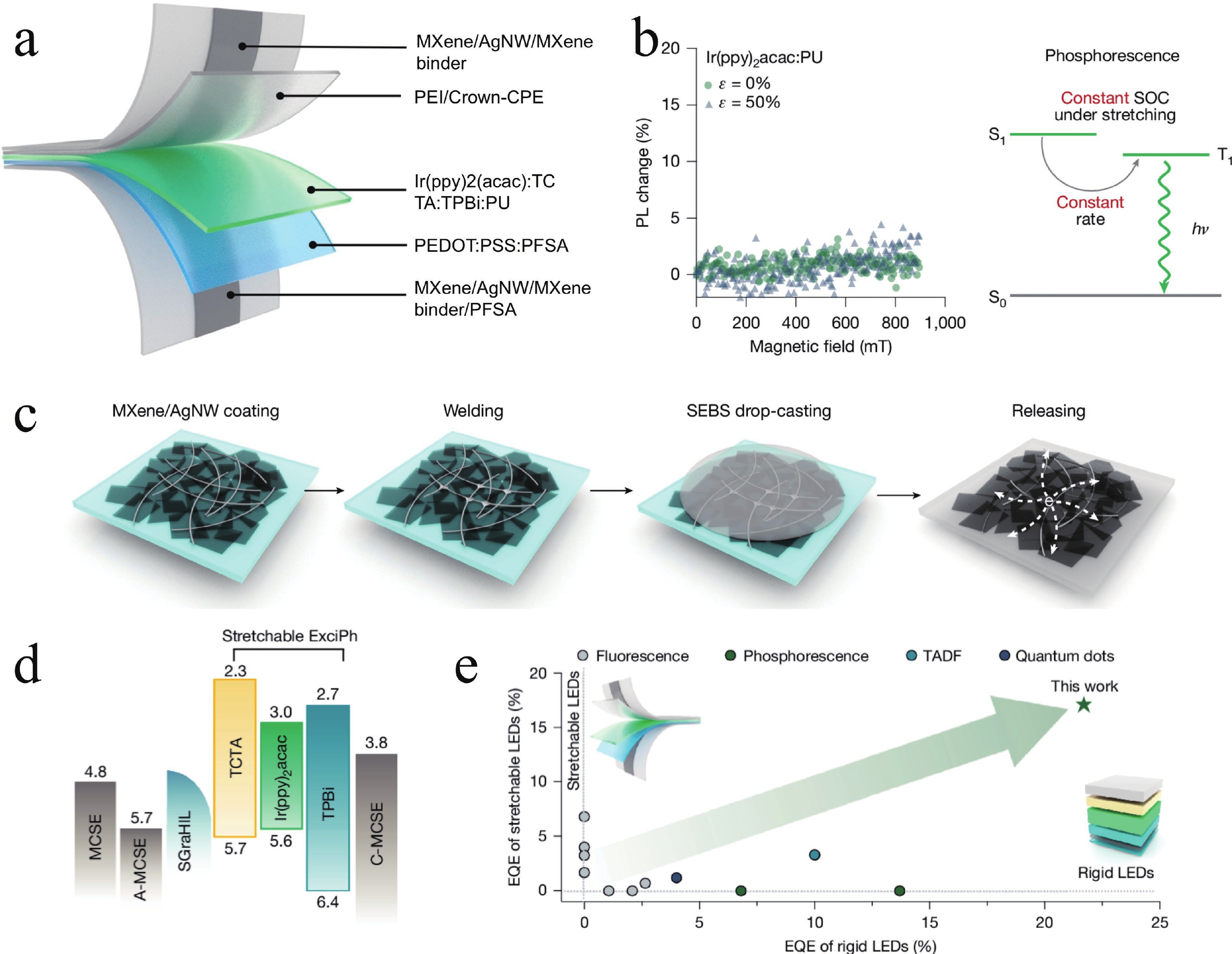
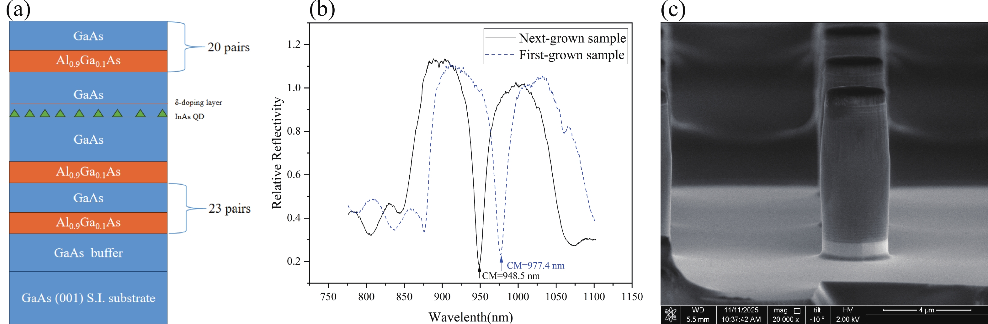
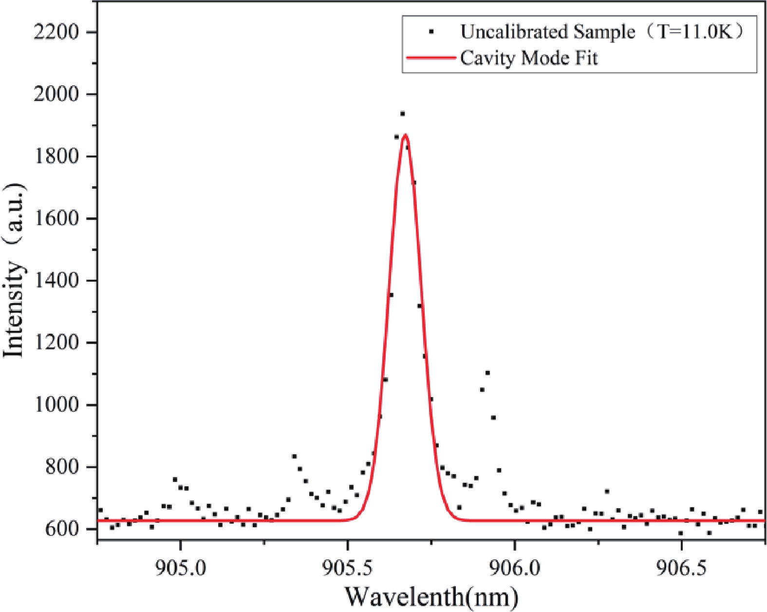
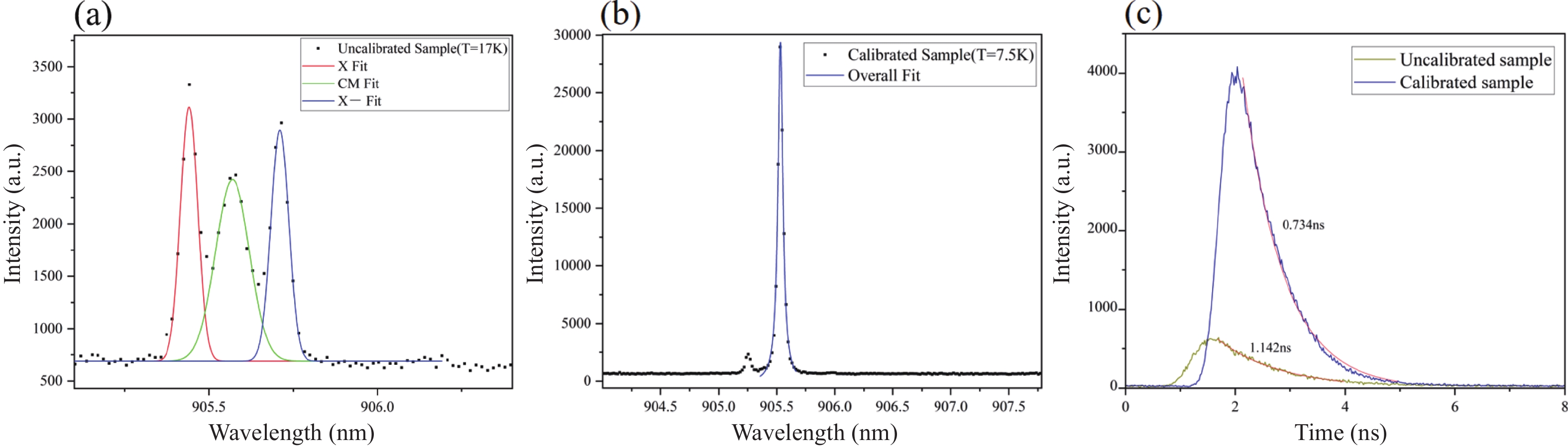
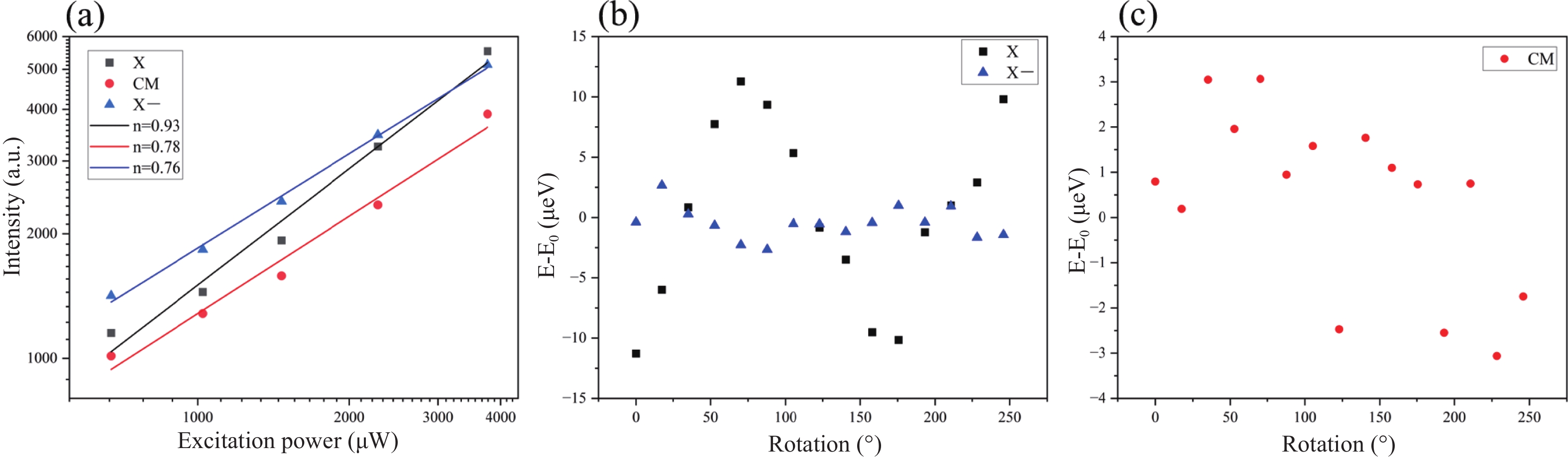
Charged quantum dots (QD) coupled to micropillar cavities are key platforms for studying photon-spin interactions. However, most research involves quantum dots charged via external excitation, resulting in short charge lifetimes. We demonstrate a device where a quantum dot confines an extra electron through δ-doping and couples to a high Q-factor (about 11 000) micropillar cavity mode (CM). We propose a precise calibration process for the micropillar cavity to achieve coupling between the negatively charged exciton (X−) transitions and CM at low temperatures. Micro-photoluminescence (μPL) spectroscopy confirms X− transitions and their coupling with CM at 7 K, with the coupled emission intensity enhanced about tenfold relative to the uncoupled state. The X− transitions and CM both show low spectral fluctuations at the change of polarization of incident light (X− 2.66 μeV, CM 3 μeV).
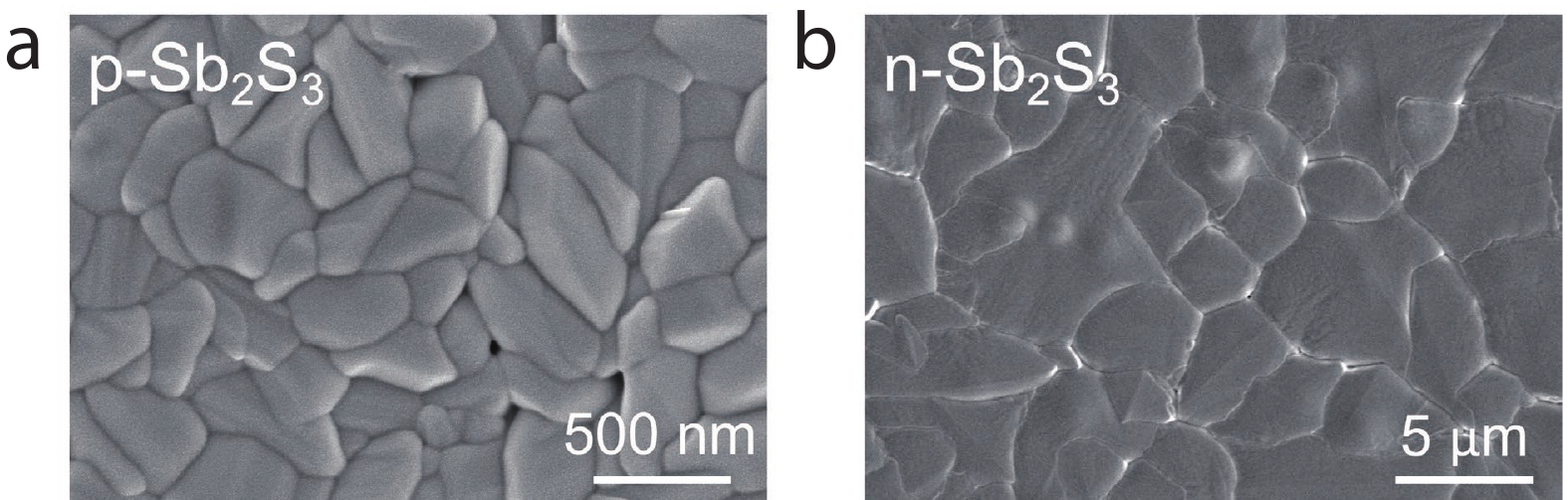
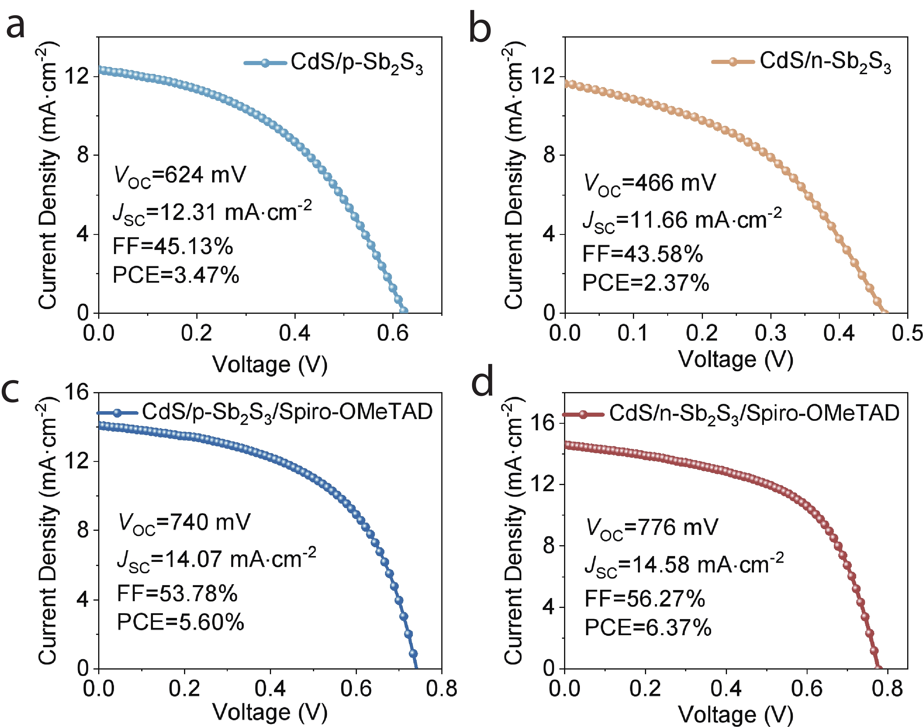
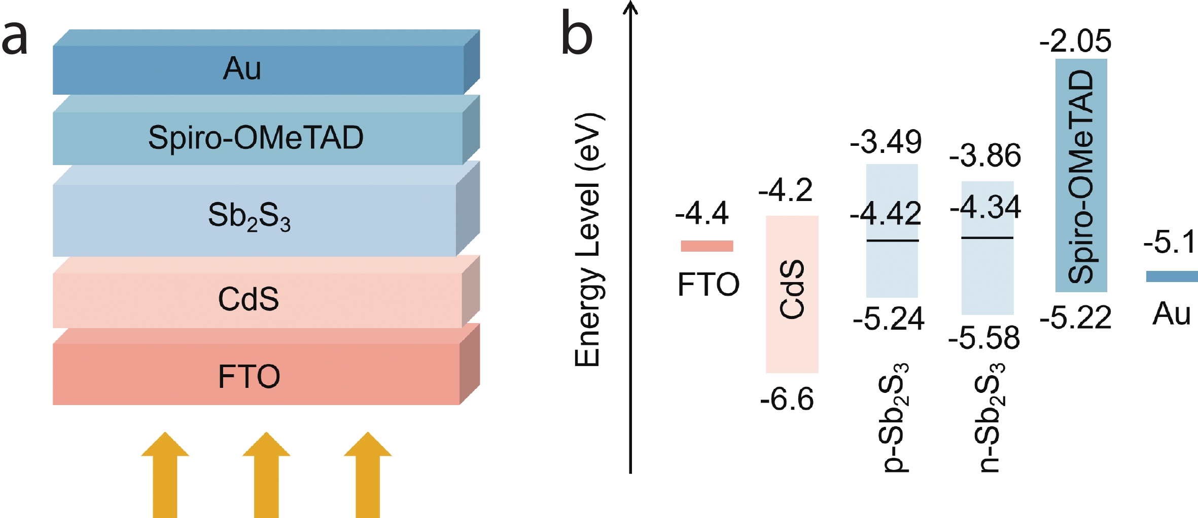
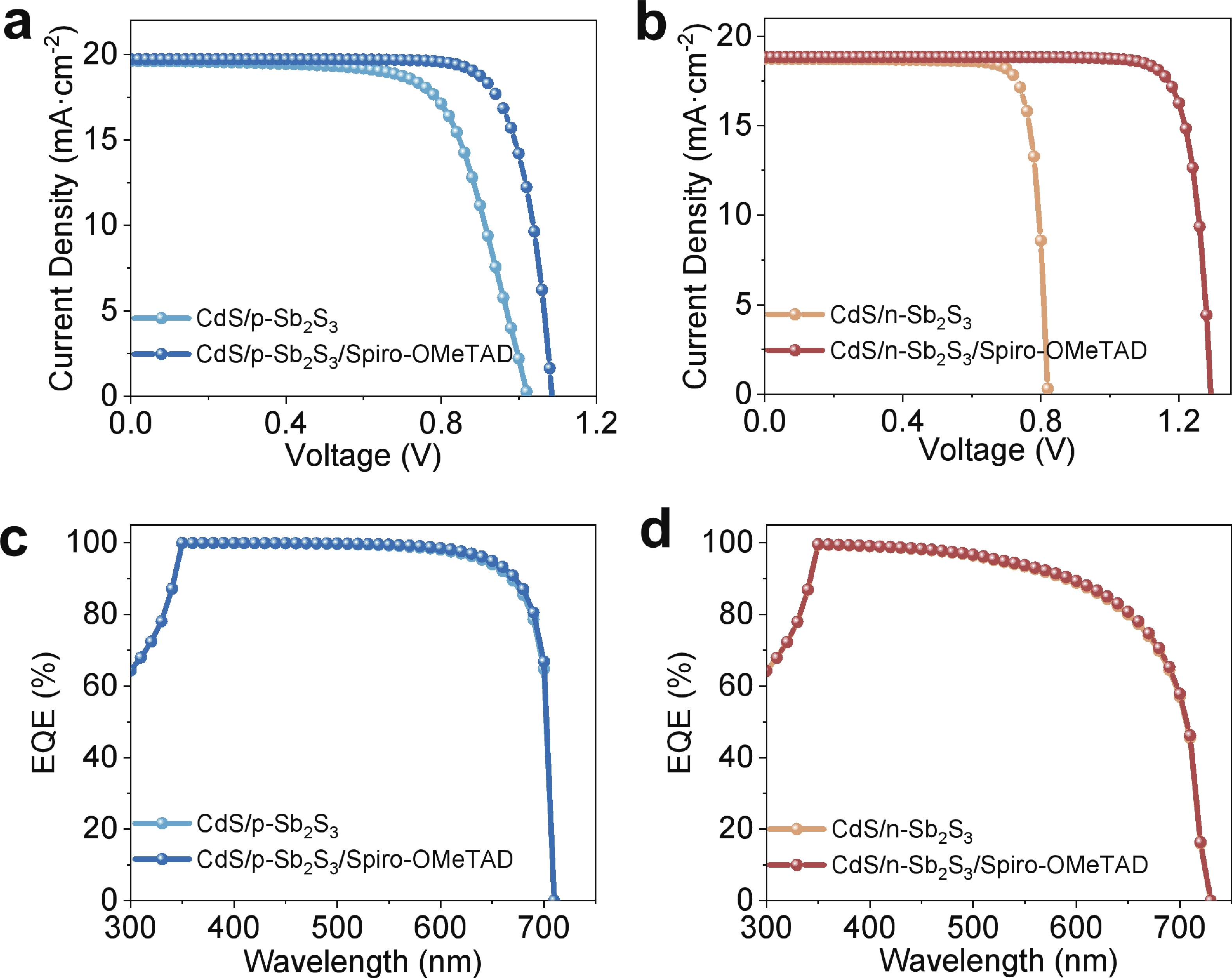
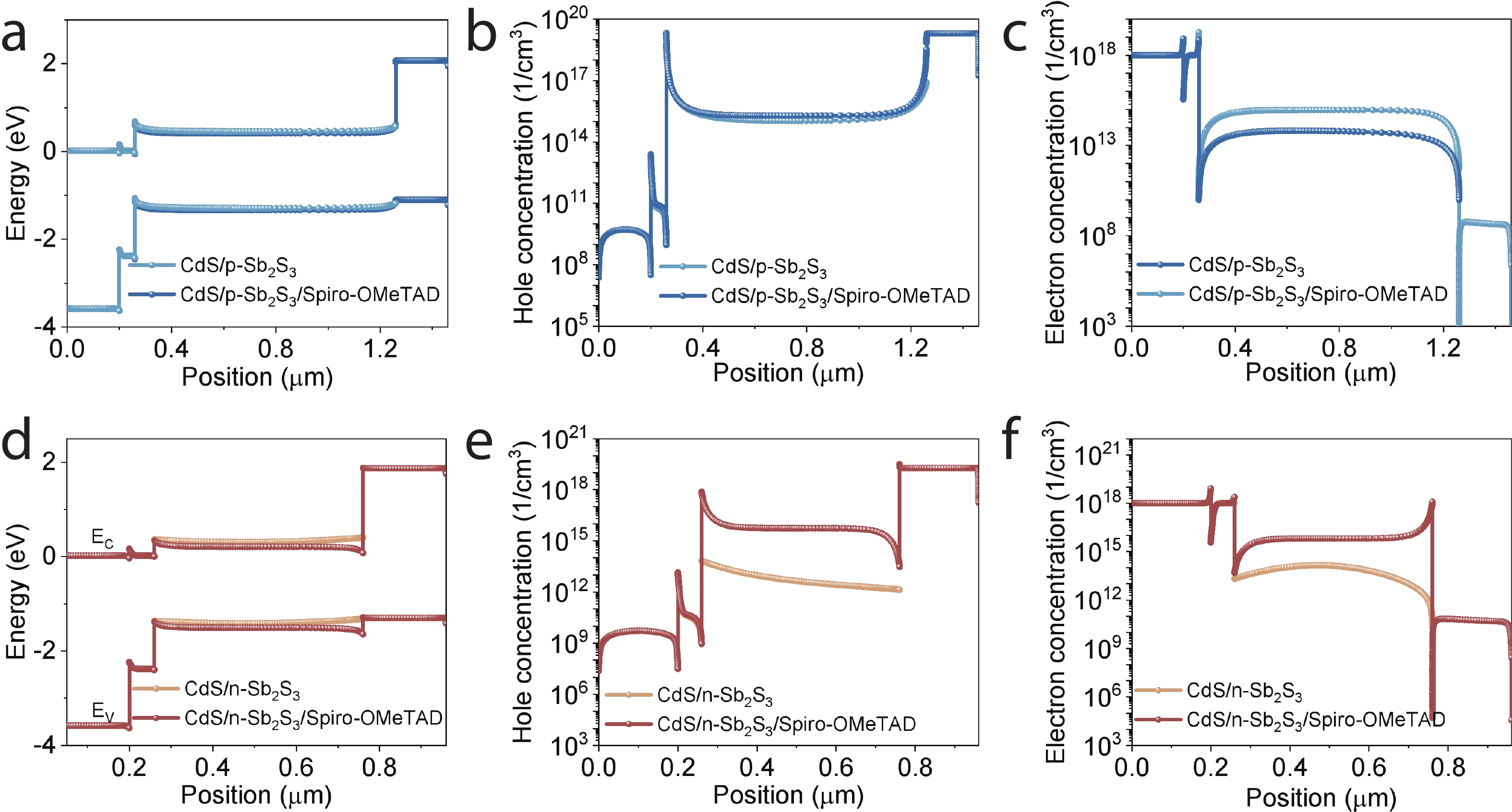
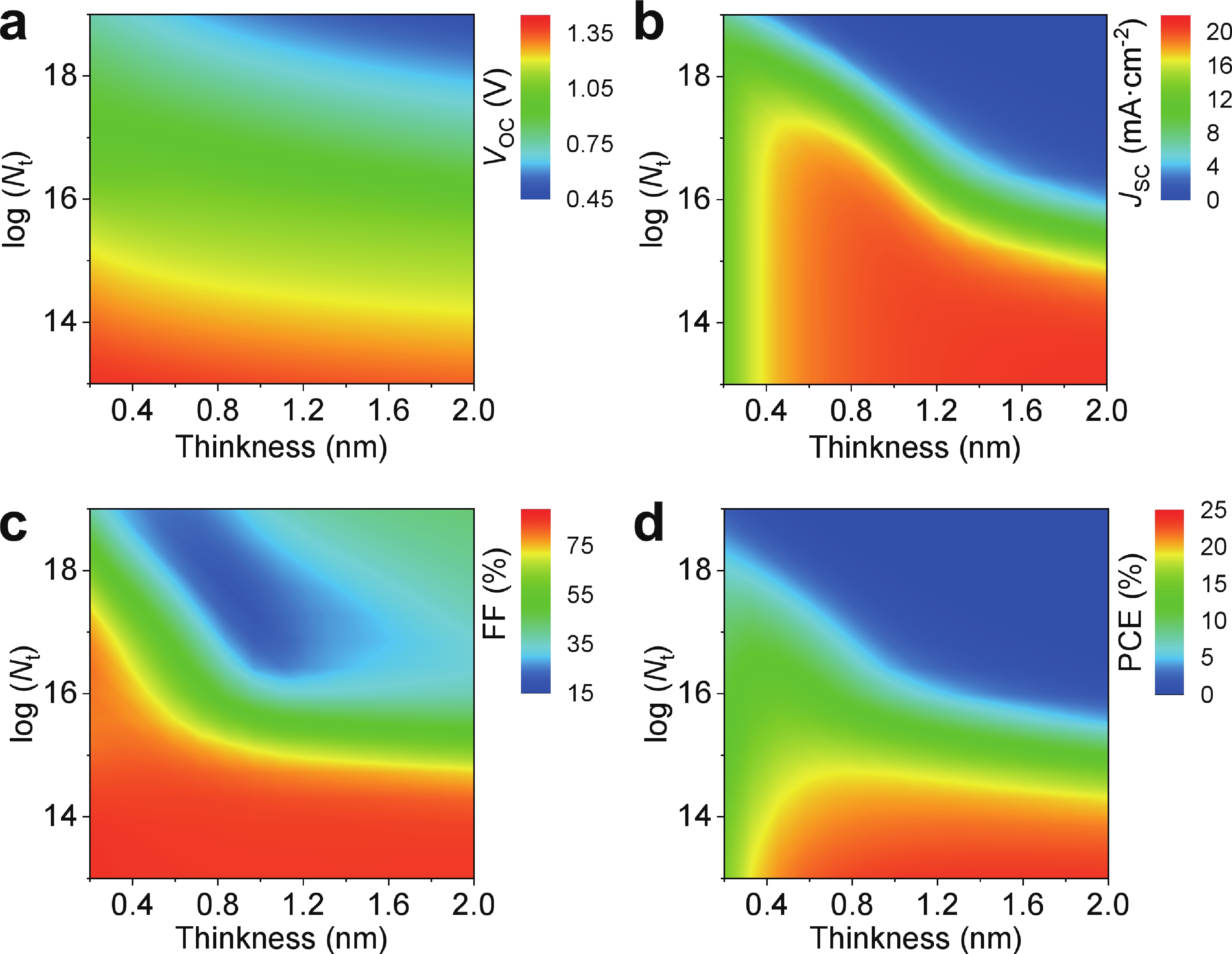
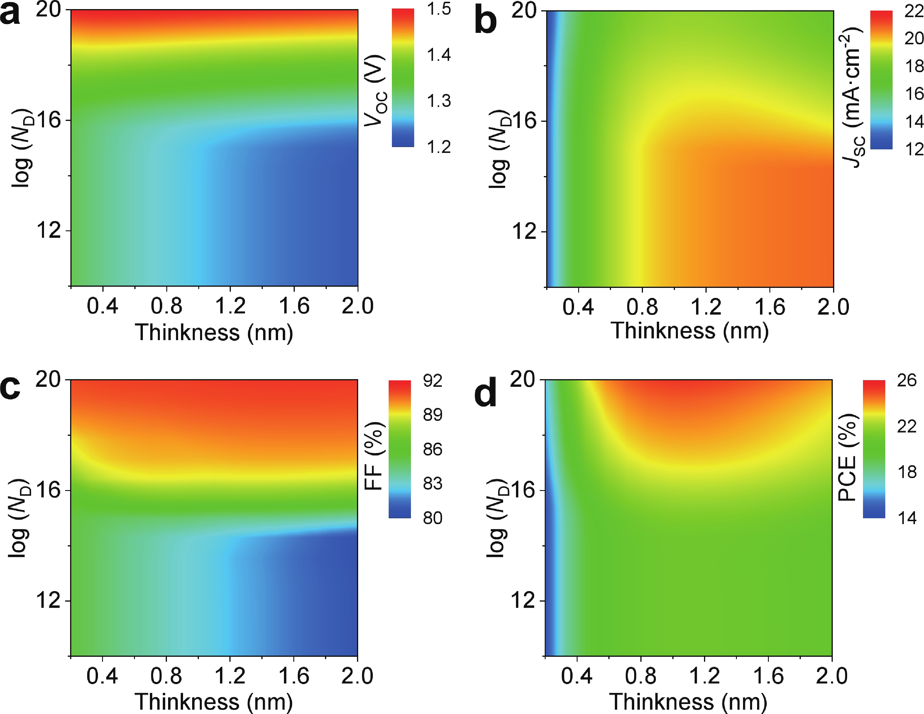
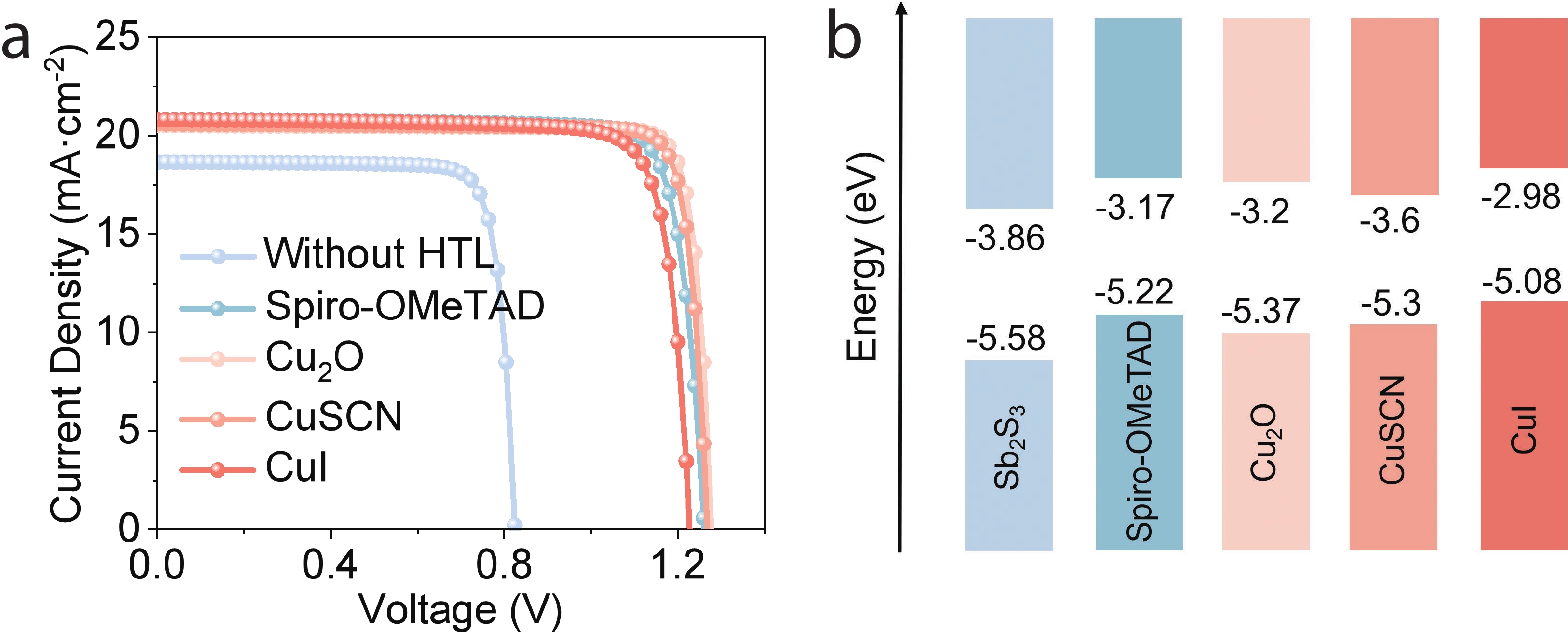
Scrutinizing the important roles of hole transport layers in near-intrinsic Sb2S3 planar solar cells
J. Semicond.
2026, 47(6): 062703 doi: 10.1088/1674-4926/25120025
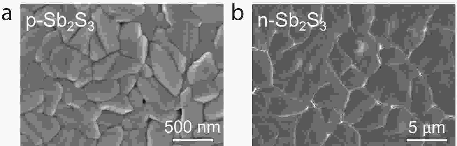
Sb2S3 has attracted increasing attention for next-generation photovoltaics due to its excellent materials and optoelectronic properties, especially a suitable bandgap (~1.75 eV) for indoor photovoltaics and silicon-based tandem solar cells. However, the highest power conversion efficiency (PCE) report thus far for Sb2S3 solar cells is 8.26%, lagging far behind its theoretical efficiency limit (~28%). This study aims to scrutinize the important roles of hole transport layers (HTLs) in near-intrinsic Sb2S3 solar cells. It is found that the device efficiencies of both of p-type Sb2S3 and n-type Sb2S3 based planar solar cells are significantly enhanced with the incorporation of Spiro-OMeTAD HTL, further confirmed by the SCAPS simulation. The specific roles of HTL on promoting the interface hole extraction in Sb2S3 solar cells are elucidated. Then the performance optimization is conducted by systematically optimizing key parameters of Sb2S3 absorbers, such as absorber thickness, defect density, and doping concentration. Furthermore, several typical inorganic HTL candidates for replacing Spiro-OMeTAD were explored for Sb2S3 solar cells, revealing that the Cu2O HTL based device exhibits a highest PCE of 23.09%. This work highlights the necessity of HTLs for devices based on near-intrinsic Sb2S3 and provides valuable insights for further enhancing the performance of Sb2S3 solar cells.