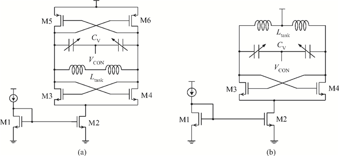
Fig. 1.
(a) Complementary cross-coupled VCO. (b) All NMOS cross-coupled VCO.
SEMICONDUCTOR INTEGRATED CIRCUITS
Xin Tang, Fengyi Huang, Xusheng Tang and Mingchi Shao
Corresponding author: Tang Xin, tang04002516@gmail.com
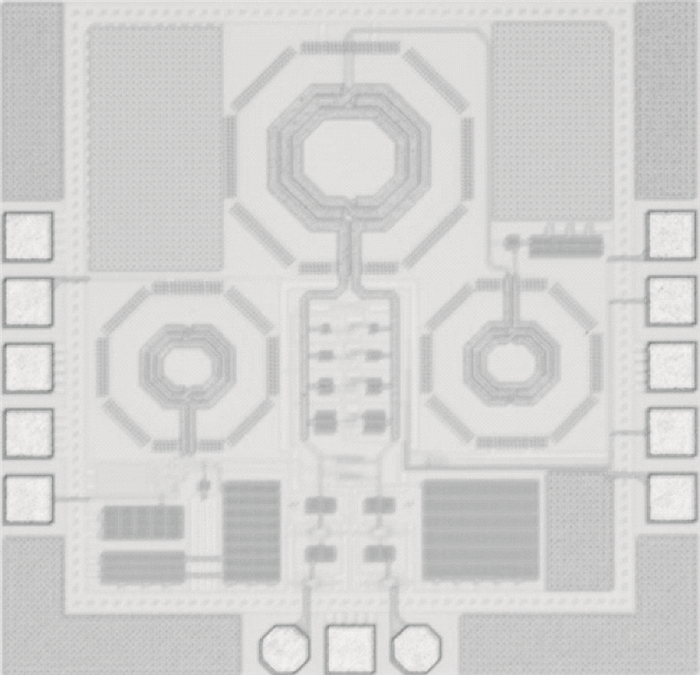
Abstract: This paper presents an LC voltage controlled oscillator (VCO) in a dual-band frequency synthesizer for IMT-advanced and UWB applications. The switched current source, cross-coupled pair and noise filtering technique are adopted in this VCO design to improve the performance of the phase noise, power consumption, voltage amplitude, and tuning range. In order to achieve a wide tuning range, a reconfigurable LC tank with 4 bits switch control is adopted in the core circuit design. The size of the entire chip with pad is 1.11×0.98 mm2. The test results show that the current dissipation of the VCO at UWB and IMT-Advanced band is 3 mA and 4.5 mA in a 1.2 V supply. The tuning range of the designed VCO is 3.86-5.28 GHz and 3.14-3.88 GHz. The phase-noise at 1 MHz frequency offset from a 3.5 GHz and 4.2 GHz carrier is-123 dBc/Hz and-119 dBc/Hz, respectively.
Keywords: LC VCO, voltage controlled oscillator, phase noise, CMOS, UWB, IMT-advanced
| [1] |
Hu X R. Design and realization of dual-band VCO for IMT-advanced and UWB systems. Master Thesis of Southeast University, 2010:1 http://www.sciencedirect.com/science/article/pii/S0924424708000897
|
| [2] |
Gao P J, Oh N J, Min H. An enhanced close-in phase noise LC-VCO using parasitic V-NPN transistors in a CMOS process. Journal of Semiconductors, 2009, 30(8):085004 doi: 10.1088/1674-4926/30/8/085004
|
| [3] |
Ismail A, Abidi A. A CMOS differential LC oscillator with suppressed up-converted flicker noise. IEEE Int Solid-State Circuits Conf, Dig Tech Papers, 2003, 1:98 doi: 10.1109/ISSCC.2003.1234224
|
| [4] |
Hajimiri A, Lee T H. A general theory of phase noise in electrical oscillators. IEEE J Solid-State Circuits, 1998, 33:179 doi: 10.1109/4.658619
|
| [5] |
Hajimiri A, Lee T H. Design issues in CMOS differential LC oscillators. IEEE J Solid-State Circuits, 1999, 34(5):717 doi: 10.1109/4.760384
|
| [6] |
Chan C F, Tang S K, Pun K P. A 4-GHz VCO for multiband OFDM UWB systems. IEEE International Conference on Electron Devices and Solid-State Circuits, 2008:1 http://ieeexplore.ieee.org/document/4760742/
|
| [7] |
Tsai M D, Cho Y H, Wang H. A 5-GHz low phase noise differential colpitts CMOS VCO. IEEE Microw Wireless Compon Lett, 2005, 15(5):327 doi: 10.1109/LMWC.2005.847696
|
| [8] |
Fong N H W, Plouchart J O, Zamdmer N, et al. Design of wide-band CMOS VCO for multiband wireless LAN applications. IEEE J Solid-State Circuits, 2003, 38(8):1333 doi: 10.1109/JSSC.2003.814440
|
| [9] |
Andreani P, Mattisson S. On the use of MOS varactors in RF VCOs. IEEE J Solid-State Circuits, 2000, 35(6):905 doi: 10.1109/4.845194
|
| [10] |
Levantino S, Samori C, Bonfanti A, et al. Frequency dependence on bias current in 5-GHz CMOS VCOs:impact on tuning range and flicker noise upconversion. IEEE J Solid-State Circuits, 2002, 37(8):1003 doi: 10.1109/JSSC.2002.800969
|
| [11] |
Stagni C, Italia A, Palmisano G. Wideband CMOS LC VCOs for IEEE 802.15.4a applications. Proceedings of the 3rd European Microwave Integrated Circuits Conference, 2008:246 http://ieeexplore.ieee.org/document/4772275/
|
| [12] |
De Muer B, Borremans M, Steyaert M, et al. A 2-GHz low phase noise integrated LC-VCO set with flicker noise upconversion minimization. IEEE J Solid-State Circuits, 2000, 35(7):1034 doi: 10.1109/4.848213
|
| [13] |
Chi B Y, Yu Z P, Shi B X. Analysis and design of CMOS RF integrated circuits. Beijing:Tsinghua University, 2006 http://ieeexplore.ieee.org/abstract/document/5061569/
|
| [14] |
Jiang Y W. Design and implementation of WSN frequency synthesizer and LC-VCO. Master Thesis of Southeast University, 2010 http://ieeexplore.ieee.org/document/1287755/
|
| [15] |
Yim S M, Ok K. Switched resonators and their applications in a dual-band monolithic CMOS LC-tuned VCO. IEEE Trans Microw Theory Tech, 2006, 54:74 doi: 10.1109/TMTT.2005.856102
|
| [16] |
Cao S G, Han K F, Tan X, et al. A 1.0 V differential VCO in 0.13μm CMOS technology. Journal of Semiconductors, 2011, 32(2):025010 doi: 10.1088/1674-4926/32/2/025010
|
| [17] |
Kim J H, Yoo H J. Multi-standard CMOS LC QVCO with reconfigurable LC tank and low power low phase noise quadrature generation method. IEICE Trans Fundamentals, 2006, E89-A(6):1547 doi: 10.1093/ietfec/e89-a.6.1547
|
| [18] |
Demirkan M, Bruss S P, Spencer R R. Design of wide tuning-range CMOS VCOs using switched coupled-inductors. IEEE Journal & Magazine, 2008, 43(12):1156 http://ieeexplore.ieee.org/document/4494650/
|
| [19] |
Jung J, Zhu S, Liu P, et al. 22-pJ/bit energy efficient 2.4-GHz implantable OOK transmitter for wireless biotelemetry systems:in vitro experiments using rat skin mimic. IEEE Trans Microw Theory Tech, 2010, 58(12):4102 http://ieeexplore.ieee.org/document/5625933/keywords
|
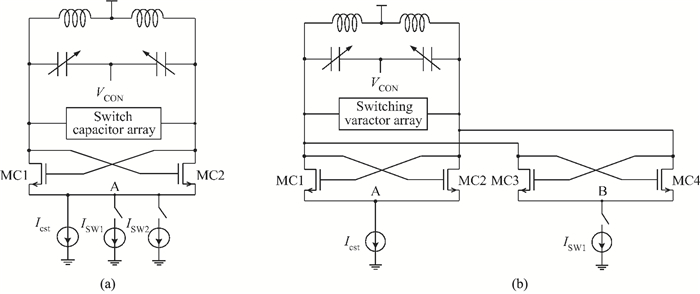
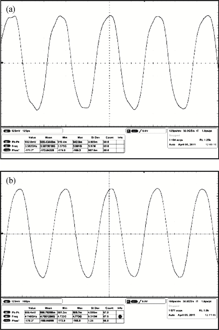
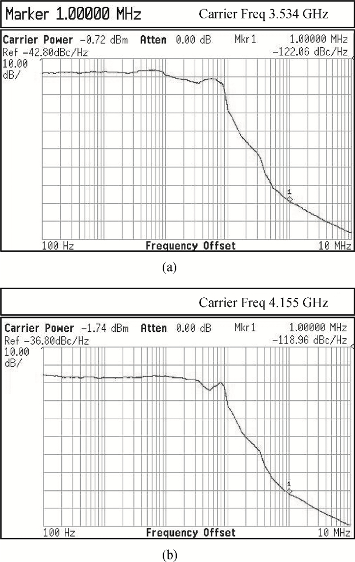
Table 1. VCO performance comparison.

|
| [1] |
Hu X R. Design and realization of dual-band VCO for IMT-advanced and UWB systems. Master Thesis of Southeast University, 2010:1 http://www.sciencedirect.com/science/article/pii/S0924424708000897
|
| [2] |
Gao P J, Oh N J, Min H. An enhanced close-in phase noise LC-VCO using parasitic V-NPN transistors in a CMOS process. Journal of Semiconductors, 2009, 30(8):085004 doi: 10.1088/1674-4926/30/8/085004
|
| [3] |
Ismail A, Abidi A. A CMOS differential LC oscillator with suppressed up-converted flicker noise. IEEE Int Solid-State Circuits Conf, Dig Tech Papers, 2003, 1:98 doi: 10.1109/ISSCC.2003.1234224
|
| [4] |
Hajimiri A, Lee T H. A general theory of phase noise in electrical oscillators. IEEE J Solid-State Circuits, 1998, 33:179 doi: 10.1109/4.658619
|
| [5] |
Hajimiri A, Lee T H. Design issues in CMOS differential LC oscillators. IEEE J Solid-State Circuits, 1999, 34(5):717 doi: 10.1109/4.760384
|
| [6] |
Chan C F, Tang S K, Pun K P. A 4-GHz VCO for multiband OFDM UWB systems. IEEE International Conference on Electron Devices and Solid-State Circuits, 2008:1 http://ieeexplore.ieee.org/document/4760742/
|
| [7] |
Tsai M D, Cho Y H, Wang H. A 5-GHz low phase noise differential colpitts CMOS VCO. IEEE Microw Wireless Compon Lett, 2005, 15(5):327 doi: 10.1109/LMWC.2005.847696
|
| [8] |
Fong N H W, Plouchart J O, Zamdmer N, et al. Design of wide-band CMOS VCO for multiband wireless LAN applications. IEEE J Solid-State Circuits, 2003, 38(8):1333 doi: 10.1109/JSSC.2003.814440
|
| [9] |
Andreani P, Mattisson S. On the use of MOS varactors in RF VCOs. IEEE J Solid-State Circuits, 2000, 35(6):905 doi: 10.1109/4.845194
|
| [10] |
Levantino S, Samori C, Bonfanti A, et al. Frequency dependence on bias current in 5-GHz CMOS VCOs:impact on tuning range and flicker noise upconversion. IEEE J Solid-State Circuits, 2002, 37(8):1003 doi: 10.1109/JSSC.2002.800969
|
| [11] |
Stagni C, Italia A, Palmisano G. Wideband CMOS LC VCOs for IEEE 802.15.4a applications. Proceedings of the 3rd European Microwave Integrated Circuits Conference, 2008:246 http://ieeexplore.ieee.org/document/4772275/
|
| [12] |
De Muer B, Borremans M, Steyaert M, et al. A 2-GHz low phase noise integrated LC-VCO set with flicker noise upconversion minimization. IEEE J Solid-State Circuits, 2000, 35(7):1034 doi: 10.1109/4.848213
|
| [13] |
Chi B Y, Yu Z P, Shi B X. Analysis and design of CMOS RF integrated circuits. Beijing:Tsinghua University, 2006 http://ieeexplore.ieee.org/abstract/document/5061569/
|
| [14] |
Jiang Y W. Design and implementation of WSN frequency synthesizer and LC-VCO. Master Thesis of Southeast University, 2010 http://ieeexplore.ieee.org/document/1287755/
|
| [15] |
Yim S M, Ok K. Switched resonators and their applications in a dual-band monolithic CMOS LC-tuned VCO. IEEE Trans Microw Theory Tech, 2006, 54:74 doi: 10.1109/TMTT.2005.856102
|
| [16] |
Cao S G, Han K F, Tan X, et al. A 1.0 V differential VCO in 0.13μm CMOS technology. Journal of Semiconductors, 2011, 32(2):025010 doi: 10.1088/1674-4926/32/2/025010
|
| [17] |
Kim J H, Yoo H J. Multi-standard CMOS LC QVCO with reconfigurable LC tank and low power low phase noise quadrature generation method. IEICE Trans Fundamentals, 2006, E89-A(6):1547 doi: 10.1093/ietfec/e89-a.6.1547
|
| [18] |
Demirkan M, Bruss S P, Spencer R R. Design of wide tuning-range CMOS VCOs using switched coupled-inductors. IEEE Journal & Magazine, 2008, 43(12):1156 http://ieeexplore.ieee.org/document/4494650/
|
| [19] |
Jung J, Zhu S, Liu P, et al. 22-pJ/bit energy efficient 2.4-GHz implantable OOK transmitter for wireless biotelemetry systems:in vitro experiments using rat skin mimic. IEEE Trans Microw Theory Tech, 2010, 58(12):4102 http://ieeexplore.ieee.org/document/5625933/keywords
|


Article views: 3592 Times PDF downloads: 36 Times Cited by: 0 Times
Received: 08 July 2012 Revised: 21 August 2012 Online: Published: 01 January 2013
| Citation: |
Xin Tang, Fengyi Huang, Xusheng Tang, Mingchi Shao. A wideband 0.13 μm CMOS LC-VCO for IMT-advanced and UWB applications[J]. Journal of Semiconductors, 2013, 34(1): 015004. doi: 10.1088/1674-4926/34/1/015004
****
X Tang, F Y Huang, X S Tang, M C Shao. A wideband 0.13 μm CMOS LC-VCO for IMT-advanced and UWB applications[J]. J. Semicond., 2013, 34(1): 015004. doi: 10.1088/1674-4926/34/1/015004.

|
| [1] |
Hu X R. Design and realization of dual-band VCO for IMT-advanced and UWB systems. Master Thesis of Southeast University, 2010:1 http://www.sciencedirect.com/science/article/pii/S0924424708000897
|
| [2] |
Gao P J, Oh N J, Min H. An enhanced close-in phase noise LC-VCO using parasitic V-NPN transistors in a CMOS process. Journal of Semiconductors, 2009, 30(8):085004 doi: 10.1088/1674-4926/30/8/085004
|
| [3] |
Ismail A, Abidi A. A CMOS differential LC oscillator with suppressed up-converted flicker noise. IEEE Int Solid-State Circuits Conf, Dig Tech Papers, 2003, 1:98 doi: 10.1109/ISSCC.2003.1234224
|
| [4] |
Hajimiri A, Lee T H. A general theory of phase noise in electrical oscillators. IEEE J Solid-State Circuits, 1998, 33:179 doi: 10.1109/4.658619
|
| [5] |
Hajimiri A, Lee T H. Design issues in CMOS differential LC oscillators. IEEE J Solid-State Circuits, 1999, 34(5):717 doi: 10.1109/4.760384
|
| [6] |
Chan C F, Tang S K, Pun K P. A 4-GHz VCO for multiband OFDM UWB systems. IEEE International Conference on Electron Devices and Solid-State Circuits, 2008:1 http://ieeexplore.ieee.org/document/4760742/
|
| [7] |
Tsai M D, Cho Y H, Wang H. A 5-GHz low phase noise differential colpitts CMOS VCO. IEEE Microw Wireless Compon Lett, 2005, 15(5):327 doi: 10.1109/LMWC.2005.847696
|
| [8] |
Fong N H W, Plouchart J O, Zamdmer N, et al. Design of wide-band CMOS VCO for multiband wireless LAN applications. IEEE J Solid-State Circuits, 2003, 38(8):1333 doi: 10.1109/JSSC.2003.814440
|
| [9] |
Andreani P, Mattisson S. On the use of MOS varactors in RF VCOs. IEEE J Solid-State Circuits, 2000, 35(6):905 doi: 10.1109/4.845194
|
| [10] |
Levantino S, Samori C, Bonfanti A, et al. Frequency dependence on bias current in 5-GHz CMOS VCOs:impact on tuning range and flicker noise upconversion. IEEE J Solid-State Circuits, 2002, 37(8):1003 doi: 10.1109/JSSC.2002.800969
|
| [11] |
Stagni C, Italia A, Palmisano G. Wideband CMOS LC VCOs for IEEE 802.15.4a applications. Proceedings of the 3rd European Microwave Integrated Circuits Conference, 2008:246 http://ieeexplore.ieee.org/document/4772275/
|
| [12] |
De Muer B, Borremans M, Steyaert M, et al. A 2-GHz low phase noise integrated LC-VCO set with flicker noise upconversion minimization. IEEE J Solid-State Circuits, 2000, 35(7):1034 doi: 10.1109/4.848213
|
| [13] |
Chi B Y, Yu Z P, Shi B X. Analysis and design of CMOS RF integrated circuits. Beijing:Tsinghua University, 2006 http://ieeexplore.ieee.org/abstract/document/5061569/
|
| [14] |
Jiang Y W. Design and implementation of WSN frequency synthesizer and LC-VCO. Master Thesis of Southeast University, 2010 http://ieeexplore.ieee.org/document/1287755/
|
| [15] |
Yim S M, Ok K. Switched resonators and their applications in a dual-band monolithic CMOS LC-tuned VCO. IEEE Trans Microw Theory Tech, 2006, 54:74 doi: 10.1109/TMTT.2005.856102
|
| [16] |
Cao S G, Han K F, Tan X, et al. A 1.0 V differential VCO in 0.13μm CMOS technology. Journal of Semiconductors, 2011, 32(2):025010 doi: 10.1088/1674-4926/32/2/025010
|
| [17] |
Kim J H, Yoo H J. Multi-standard CMOS LC QVCO with reconfigurable LC tank and low power low phase noise quadrature generation method. IEICE Trans Fundamentals, 2006, E89-A(6):1547 doi: 10.1093/ietfec/e89-a.6.1547
|
| [18] |
Demirkan M, Bruss S P, Spencer R R. Design of wide tuning-range CMOS VCOs using switched coupled-inductors. IEEE Journal & Magazine, 2008, 43(12):1156 http://ieeexplore.ieee.org/document/4494650/
|
| [19] |
Jung J, Zhu S, Liu P, et al. 22-pJ/bit energy efficient 2.4-GHz implantable OOK transmitter for wireless biotelemetry systems:in vitro experiments using rat skin mimic. IEEE Trans Microw Theory Tech, 2010, 58(12):4102 http://ieeexplore.ieee.org/document/5625933/keywords
|

 WeChat ID
Journal of Semiconductors © 2017 All Rights Reserved 京ICP备05085259号-2

 DownLoad: