


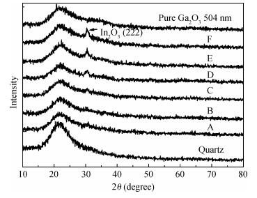
Fig. 1.
XRD patterns of Ga2O3/ITO alternating multilayer films with different repetition periods
SEMICONDUCTOR MATERIALS
Chengyang Xu, Jinliang Yan, Chao Li and Huihui Zhuang
Corresponding author: Yan Jinliang, yanjinliang@yahoo.cn
Abstract: Ga2O3/ITO alternating multilayer films were deposited on quartz glass substrates by magnetron sputtering. The effect of the multi-period on the structural, optical and electrical properties of Ga2O3/ITO alternating multilayer films was investigated by an X-ray diffractometer, a double beam spectrophotometer and the Hall system, respectively. A low sheet resistance of 225.5Ω/ꭐ and a high transmittance of more than 62.9% at a 300 nm wavelength were obtained for the two-period alternating multilayer film with a thickness of 72 nm.
Keywords: transparent conductive film, alternating multilayer film, deep ultraviolet, multi-period, gallium oxide, indium tin oxide
| [1] |
Binet L, Gourier D. Origin of the blue luminescence of β -Ga2O3. J Phys Chem Solids, 1998, 59(8):1241 doi: 10.1016/S0022-3697(98)00047-X
|
| [2] |
Orita M, Hiramatsu H, Ohta H, et al. Preparation of highly conductive, deep ultraviolet transparent β -Ga2O3 thin film at low deposition temperatures. Thin Solid Films, 2002, 411(1):134 doi: 10.1016/S0040-6090(02)00202-X
|
| [3] |
Orita M, Ohta H, Hirano M, et al. Deep-ultraviolet transparent conductive β -Ga2O3 thin films. Appl Phys Lett, 2000, 77(25):4166 doi: 10.1063/1.1330559
|
| [4] |
Ueda N, Hosono H, Waseda R, et al. Synthesis and control of conductivity of ultraviolet transmitting β -Ga2O3 single crystals. Appl Phys Lett, 1997, 70(26):3561 doi: 10.1063/1.119233
|
| [5] |
Ogita M, Higo K, Nakanishi Y, et al. Ga2O3 thin film for oxygen sensor at high temperature. Appl Phys Lett, 2001, 175/176:721 doi: 10.1186/2251-7235-6-17
|
| [6] |
Benramache S, Chabane F, Benhaoua B, et al. Influence of growth time on crystalline structure, conductivity and optical properties of ZnO thin films. Journal of Semiconductors, 2013, 34(2):023001 doi: 10.1088/1674-4926/34/2/023001
|
| [7] |
Coutts T J, Young D L, Li Xiaonan. Characterization of transparent conducting oxide. MRS Bulletin, 2000, 25(8):58 doi: 10.1557/mrs2000.152
|
| [8] |
Yue Wei, Yan Jinliang, Wu Jiangyan, et al. Structural and optical properties of Zn-doped β -Ga2O3 films. Journal of Semiconductors, 2012, 33(7):073003 doi: 10.1088/1674-4926/33/7/073003
|
| [9] |
Minami T. New n-type transparent conducting oxides. MRS Bulletin, 2000, 25(8):38 doi: 10.1557/mrs2000.149
|
| [10] |
Yang F, Ma J, Luan C, et al. Structural and optical properties of Ga2(1-x)In2xO3 films prepared on α -Al2O3 (0001) by MOCVD. Appl Surf Sci, 2009, 255(8):4401 doi: 10.1016/j.apsusc.2008.10.129
|
| [11] |
Liu Jianjun, Yan Jinliang, Shi Liang, et al. Electrical and optical properties of deep ultraviolet transparent conductive Ga2O3/ITO films by magnetron sputtering. Journal of Semiconductors, 2010, 31(10):103001 doi: 10.1088/1674-4926/31/10/103001
|
| [12] |
Li Ting, Yan Jinliang, Ding Xingwei, et al. Effect of substrate temperature on the properties of deep ultraviolet transparent conductive ITO/Ga2O3 films. Journal of Semiconductors, 2012, 33(1):013002 doi: 10.1088/1674-4926/33/1/013002
|
| [13] |
Hao L, Diao X, Xu H, et al. Thickness dependence of structural, electrical and optical properties of indium tin oxide (ITO) films deposited on PET substrates. Appl Surf Sci, 2008, 254(11):3504 doi: 10.1016/j.apsusc.2007.11.063
|
| [14] |
Cullity B D, Stock S R. Elements of X-ray diffraction. 3rd ed. New Jersey: Prentice Hall, 2001
|
| [15] |
Guillen C, Herrero J. Polycrystalline growth and recrystallization processes in sputtered ITO thin films. Thin Solid Films, 2006, 510(1/2):260 http://www.sharp-world.com/corporate/info/rd/tj3/pdf/8.pdf
|
| [16] |
Szczyrbowski J, Hartig K, Roegels S, et al. Coating, composed of an optically effective layer system, for substrates, whereby the layer system has a high anti-reflective effect, and method for the manufacturing of the coating. US Patent, No. 5216542, 1993
|
| [17] |
Ray S, Banerjee R, Basu N, et al. Properties of tin doped indium oxide thin films prepared by magnetron sputtering. J Appl Phys, 1983, 54(6):3497 doi: 10.1063/1.332415
|
| [18] |
Tauc J. Amorphous and liquid semiconductors. London:Plenum Press, 1974
|
| [19] |
Curie D, Bartolo B D. Luminescence of inorganic solids. New York:Plenum Press, 1978
|
| [20] |
Higuchi M, Uekusa S, Nakano R, et al. Postdeposition annealing influence on sputtered indium tin oxide film characteristics. Jpn J Appl Phys, 1994, 33:302 doi: 10.1143/JJAP.33.302
|
| [21] |
Seto J Y W. The electrical properties of polycrystalline silicon films. J Appl Phys, 1975, 46(12):5247 doi: 10.1063/1.321593
|
| [22] |
Kulkarni A K, Schulz K H, Lim T S, et al. Dependence of the sheet resistance of indium-tin-oxide thin films on grain size and grain orientation determined from X-ray diffraction techniques. Thin Solid Films, 1999, 345(2):273 doi: 10.1016/S0040-6090(98)01430-8
|
| [23] |
Zhang Qun, Li Xifeng, Li Guifeng. Dependence of electrical and optical properties on thickness of tungsten-doped indium oxidethin films. Thin Solid Films, 2008, 517(2):613 doi: 10.1016/j.tsf.2008.07.023
|
| [24] |
Kim H, Horwitz J S, Kushto G, et al. Effect of film thickness on the properties of indium tin oxide thin films. J Appl Phys, 2000, 88(10):6021 doi: 10.1063/1.1318368
|
| [25] |
Gao Meizhen, Job R, Xue Desheng, et al. Thickness dependence of resistivity and optical reflectance of ITO films. Chin Phys Lett, 2008, 25(4):1380 doi: 10.1088/0256-307X/25/4/059
|
| [26] |
Haacke G. New figure of merit for transparent conductors. J Appl Phys, 1976, 47(9):4086 doi: 10.1063/1.323240
|
| [27] |
Kim D. Influence of the Cs partial pressure on the optical and electrical properties of ITO films prepared by dc sputter type negative metal ion beam deposition. Opt Mater, 2003, 24(3):471 doi: 10.1016/S0925-3467(03)00030-2
|
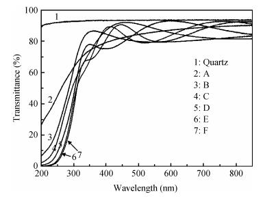
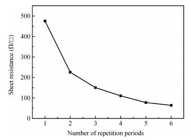
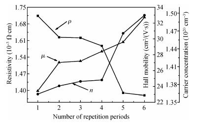
Table 1. Repetition period and total thickness of Ga2O3/ITO alternating multilayer films
 |
| [1] |
Binet L, Gourier D. Origin of the blue luminescence of β -Ga2O3. J Phys Chem Solids, 1998, 59(8):1241 doi: 10.1016/S0022-3697(98)00047-X
|
| [2] |
Orita M, Hiramatsu H, Ohta H, et al. Preparation of highly conductive, deep ultraviolet transparent β -Ga2O3 thin film at low deposition temperatures. Thin Solid Films, 2002, 411(1):134 doi: 10.1016/S0040-6090(02)00202-X
|
| [3] |
Orita M, Ohta H, Hirano M, et al. Deep-ultraviolet transparent conductive β -Ga2O3 thin films. Appl Phys Lett, 2000, 77(25):4166 doi: 10.1063/1.1330559
|
| [4] |
Ueda N, Hosono H, Waseda R, et al. Synthesis and control of conductivity of ultraviolet transmitting β -Ga2O3 single crystals. Appl Phys Lett, 1997, 70(26):3561 doi: 10.1063/1.119233
|
| [5] |
Ogita M, Higo K, Nakanishi Y, et al. Ga2O3 thin film for oxygen sensor at high temperature. Appl Phys Lett, 2001, 175/176:721 doi: 10.1186/2251-7235-6-17
|
| [6] |
Benramache S, Chabane F, Benhaoua B, et al. Influence of growth time on crystalline structure, conductivity and optical properties of ZnO thin films. Journal of Semiconductors, 2013, 34(2):023001 doi: 10.1088/1674-4926/34/2/023001
|
| [7] |
Coutts T J, Young D L, Li Xiaonan. Characterization of transparent conducting oxide. MRS Bulletin, 2000, 25(8):58 doi: 10.1557/mrs2000.152
|
| [8] |
Yue Wei, Yan Jinliang, Wu Jiangyan, et al. Structural and optical properties of Zn-doped β -Ga2O3 films. Journal of Semiconductors, 2012, 33(7):073003 doi: 10.1088/1674-4926/33/7/073003
|
| [9] |
Minami T. New n-type transparent conducting oxides. MRS Bulletin, 2000, 25(8):38 doi: 10.1557/mrs2000.149
|
| [10] |
Yang F, Ma J, Luan C, et al. Structural and optical properties of Ga2(1-x)In2xO3 films prepared on α -Al2O3 (0001) by MOCVD. Appl Surf Sci, 2009, 255(8):4401 doi: 10.1016/j.apsusc.2008.10.129
|
| [11] |
Liu Jianjun, Yan Jinliang, Shi Liang, et al. Electrical and optical properties of deep ultraviolet transparent conductive Ga2O3/ITO films by magnetron sputtering. Journal of Semiconductors, 2010, 31(10):103001 doi: 10.1088/1674-4926/31/10/103001
|
| [12] |
Li Ting, Yan Jinliang, Ding Xingwei, et al. Effect of substrate temperature on the properties of deep ultraviolet transparent conductive ITO/Ga2O3 films. Journal of Semiconductors, 2012, 33(1):013002 doi: 10.1088/1674-4926/33/1/013002
|
| [13] |
Hao L, Diao X, Xu H, et al. Thickness dependence of structural, electrical and optical properties of indium tin oxide (ITO) films deposited on PET substrates. Appl Surf Sci, 2008, 254(11):3504 doi: 10.1016/j.apsusc.2007.11.063
|
| [14] |
Cullity B D, Stock S R. Elements of X-ray diffraction. 3rd ed. New Jersey: Prentice Hall, 2001
|
| [15] |
Guillen C, Herrero J. Polycrystalline growth and recrystallization processes in sputtered ITO thin films. Thin Solid Films, 2006, 510(1/2):260 http://www.sharp-world.com/corporate/info/rd/tj3/pdf/8.pdf
|
| [16] |
Szczyrbowski J, Hartig K, Roegels S, et al. Coating, composed of an optically effective layer system, for substrates, whereby the layer system has a high anti-reflective effect, and method for the manufacturing of the coating. US Patent, No. 5216542, 1993
|
| [17] |
Ray S, Banerjee R, Basu N, et al. Properties of tin doped indium oxide thin films prepared by magnetron sputtering. J Appl Phys, 1983, 54(6):3497 doi: 10.1063/1.332415
|
| [18] |
Tauc J. Amorphous and liquid semiconductors. London:Plenum Press, 1974
|
| [19] |
Curie D, Bartolo B D. Luminescence of inorganic solids. New York:Plenum Press, 1978
|
| [20] |
Higuchi M, Uekusa S, Nakano R, et al. Postdeposition annealing influence on sputtered indium tin oxide film characteristics. Jpn J Appl Phys, 1994, 33:302 doi: 10.1143/JJAP.33.302
|
| [21] |
Seto J Y W. The electrical properties of polycrystalline silicon films. J Appl Phys, 1975, 46(12):5247 doi: 10.1063/1.321593
|
| [22] |
Kulkarni A K, Schulz K H, Lim T S, et al. Dependence of the sheet resistance of indium-tin-oxide thin films on grain size and grain orientation determined from X-ray diffraction techniques. Thin Solid Films, 1999, 345(2):273 doi: 10.1016/S0040-6090(98)01430-8
|
| [23] |
Zhang Qun, Li Xifeng, Li Guifeng. Dependence of electrical and optical properties on thickness of tungsten-doped indium oxidethin films. Thin Solid Films, 2008, 517(2):613 doi: 10.1016/j.tsf.2008.07.023
|
| [24] |
Kim H, Horwitz J S, Kushto G, et al. Effect of film thickness on the properties of indium tin oxide thin films. J Appl Phys, 2000, 88(10):6021 doi: 10.1063/1.1318368
|
| [25] |
Gao Meizhen, Job R, Xue Desheng, et al. Thickness dependence of resistivity and optical reflectance of ITO films. Chin Phys Lett, 2008, 25(4):1380 doi: 10.1088/0256-307X/25/4/059
|
| [26] |
Haacke G. New figure of merit for transparent conductors. J Appl Phys, 1976, 47(9):4086 doi: 10.1063/1.323240
|
| [27] |
Kim D. Influence of the Cs partial pressure on the optical and electrical properties of ITO films prepared by dc sputter type negative metal ion beam deposition. Opt Mater, 2003, 24(3):471 doi: 10.1016/S0925-3467(03)00030-2
|


Article views: 3205 Times PDF downloads: 22 Times Cited by: 0 Times
Received: 18 March 2013 Revised: 16 April 2013 Online: Published: 01 October 2013
| Citation: |
Chengyang Xu, Jinliang Yan, Chao Li, Huihui Zhuang. The effect of the multi-period on the properties of deep-ultraviolet transparent conductive Ga2O3/ITO alternating multilayer films[J]. Journal of Semiconductors, 2013, 34(10): 103004. doi: 10.1088/1674-4926/34/10/103004
****
C Y Xu, J L Yan, C Li, H H Zhuang. The effect of the multi-period on the properties of deep-ultraviolet transparent conductive Ga2O3/ITO alternating multilayer films[J]. J. Semicond., 2013, 34(10): 103004. doi: 10.1088/1674-4926/34/10/103004.

|
| [1] |
Binet L, Gourier D. Origin of the blue luminescence of β -Ga2O3. J Phys Chem Solids, 1998, 59(8):1241 doi: 10.1016/S0022-3697(98)00047-X
|
| [2] |
Orita M, Hiramatsu H, Ohta H, et al. Preparation of highly conductive, deep ultraviolet transparent β -Ga2O3 thin film at low deposition temperatures. Thin Solid Films, 2002, 411(1):134 doi: 10.1016/S0040-6090(02)00202-X
|
| [3] |
Orita M, Ohta H, Hirano M, et al. Deep-ultraviolet transparent conductive β -Ga2O3 thin films. Appl Phys Lett, 2000, 77(25):4166 doi: 10.1063/1.1330559
|
| [4] |
Ueda N, Hosono H, Waseda R, et al. Synthesis and control of conductivity of ultraviolet transmitting β -Ga2O3 single crystals. Appl Phys Lett, 1997, 70(26):3561 doi: 10.1063/1.119233
|
| [5] |
Ogita M, Higo K, Nakanishi Y, et al. Ga2O3 thin film for oxygen sensor at high temperature. Appl Phys Lett, 2001, 175/176:721 doi: 10.1186/2251-7235-6-17
|
| [6] |
Benramache S, Chabane F, Benhaoua B, et al. Influence of growth time on crystalline structure, conductivity and optical properties of ZnO thin films. Journal of Semiconductors, 2013, 34(2):023001 doi: 10.1088/1674-4926/34/2/023001
|
| [7] |
Coutts T J, Young D L, Li Xiaonan. Characterization of transparent conducting oxide. MRS Bulletin, 2000, 25(8):58 doi: 10.1557/mrs2000.152
|
| [8] |
Yue Wei, Yan Jinliang, Wu Jiangyan, et al. Structural and optical properties of Zn-doped β -Ga2O3 films. Journal of Semiconductors, 2012, 33(7):073003 doi: 10.1088/1674-4926/33/7/073003
|
| [9] |
Minami T. New n-type transparent conducting oxides. MRS Bulletin, 2000, 25(8):38 doi: 10.1557/mrs2000.149
|
| [10] |
Yang F, Ma J, Luan C, et al. Structural and optical properties of Ga2(1-x)In2xO3 films prepared on α -Al2O3 (0001) by MOCVD. Appl Surf Sci, 2009, 255(8):4401 doi: 10.1016/j.apsusc.2008.10.129
|
| [11] |
Liu Jianjun, Yan Jinliang, Shi Liang, et al. Electrical and optical properties of deep ultraviolet transparent conductive Ga2O3/ITO films by magnetron sputtering. Journal of Semiconductors, 2010, 31(10):103001 doi: 10.1088/1674-4926/31/10/103001
|
| [12] |
Li Ting, Yan Jinliang, Ding Xingwei, et al. Effect of substrate temperature on the properties of deep ultraviolet transparent conductive ITO/Ga2O3 films. Journal of Semiconductors, 2012, 33(1):013002 doi: 10.1088/1674-4926/33/1/013002
|
| [13] |
Hao L, Diao X, Xu H, et al. Thickness dependence of structural, electrical and optical properties of indium tin oxide (ITO) films deposited on PET substrates. Appl Surf Sci, 2008, 254(11):3504 doi: 10.1016/j.apsusc.2007.11.063
|
| [14] |
Cullity B D, Stock S R. Elements of X-ray diffraction. 3rd ed. New Jersey: Prentice Hall, 2001
|
| [15] |
Guillen C, Herrero J. Polycrystalline growth and recrystallization processes in sputtered ITO thin films. Thin Solid Films, 2006, 510(1/2):260 http://www.sharp-world.com/corporate/info/rd/tj3/pdf/8.pdf
|
| [16] |
Szczyrbowski J, Hartig K, Roegels S, et al. Coating, composed of an optically effective layer system, for substrates, whereby the layer system has a high anti-reflective effect, and method for the manufacturing of the coating. US Patent, No. 5216542, 1993
|
| [17] |
Ray S, Banerjee R, Basu N, et al. Properties of tin doped indium oxide thin films prepared by magnetron sputtering. J Appl Phys, 1983, 54(6):3497 doi: 10.1063/1.332415
|
| [18] |
Tauc J. Amorphous and liquid semiconductors. London:Plenum Press, 1974
|
| [19] |
Curie D, Bartolo B D. Luminescence of inorganic solids. New York:Plenum Press, 1978
|
| [20] |
Higuchi M, Uekusa S, Nakano R, et al. Postdeposition annealing influence on sputtered indium tin oxide film characteristics. Jpn J Appl Phys, 1994, 33:302 doi: 10.1143/JJAP.33.302
|
| [21] |
Seto J Y W. The electrical properties of polycrystalline silicon films. J Appl Phys, 1975, 46(12):5247 doi: 10.1063/1.321593
|
| [22] |
Kulkarni A K, Schulz K H, Lim T S, et al. Dependence of the sheet resistance of indium-tin-oxide thin films on grain size and grain orientation determined from X-ray diffraction techniques. Thin Solid Films, 1999, 345(2):273 doi: 10.1016/S0040-6090(98)01430-8
|
| [23] |
Zhang Qun, Li Xifeng, Li Guifeng. Dependence of electrical and optical properties on thickness of tungsten-doped indium oxidethin films. Thin Solid Films, 2008, 517(2):613 doi: 10.1016/j.tsf.2008.07.023
|
| [24] |
Kim H, Horwitz J S, Kushto G, et al. Effect of film thickness on the properties of indium tin oxide thin films. J Appl Phys, 2000, 88(10):6021 doi: 10.1063/1.1318368
|
| [25] |
Gao Meizhen, Job R, Xue Desheng, et al. Thickness dependence of resistivity and optical reflectance of ITO films. Chin Phys Lett, 2008, 25(4):1380 doi: 10.1088/0256-307X/25/4/059
|
| [26] |
Haacke G. New figure of merit for transparent conductors. J Appl Phys, 1976, 47(9):4086 doi: 10.1063/1.323240
|
| [27] |
Kim D. Influence of the Cs partial pressure on the optical and electrical properties of ITO films prepared by dc sputter type negative metal ion beam deposition. Opt Mater, 2003, 24(3):471 doi: 10.1016/S0925-3467(03)00030-2
|

 WeChat ID
Journal of Semiconductors © 2017 All Rights Reserved 京ICP备05085259号-2

 DownLoad:

