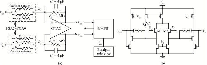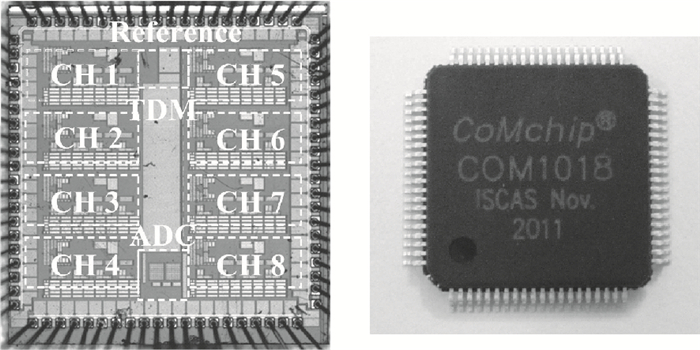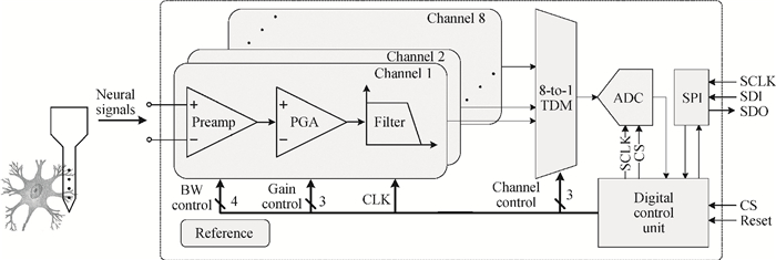
Fig. 1.
Architecture of the multi-channel neural recording chip.
SEMICONDUCTOR INTEGRATED CIRCUITS
Yun Gui1, Xu Zhang1, , Yuan Wang1, Ming Liu1, Weihua Pei1, Kai Liang2, Suibiao Huang2, Bin Li2 and Hongda Chen1
Corresponding author: Zhang Xu, zhangxu@semi.ac.cn
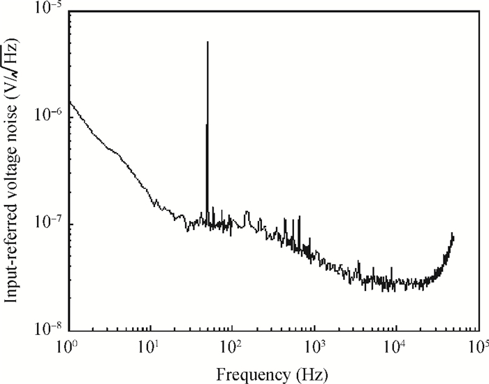
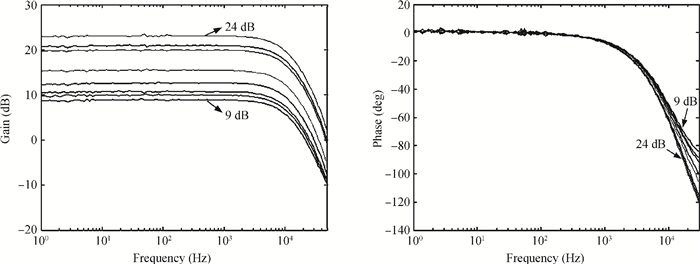
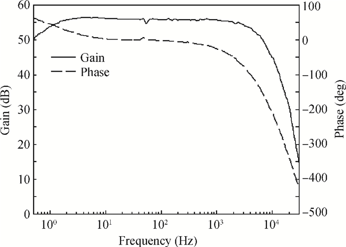
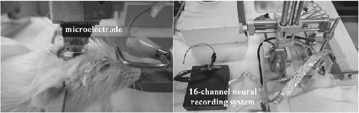
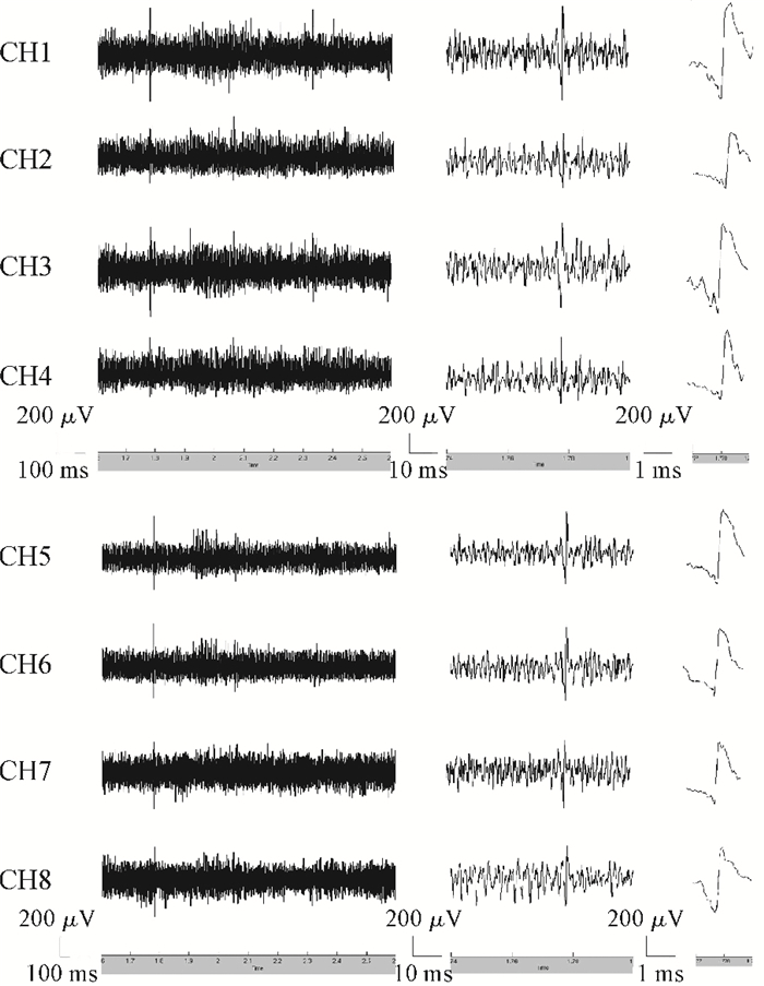
Abstract: A multi-channel, fully differential programmable chip for neural recording application is presented. The integrated circuit incorporates eight neural recording amplifiers with tunable bandwidth and gain, eight 4th-order Bessel switch capacitor filters, an 8-to-1 analog time-division multiplexer, a fully differential successive approximation register analog-to-digital converter (SAR ADC), and a serial peripheral interface for communication. The neural recording amplifier presents a programmable gain from 53 dB to 68 dB, a tunable low cut-off frequency from 0.1 Hz to 300 Hz, and 3.77 μVrms input-referred noise over a 5 kHz bandwidth. The SAR ADC digitizes signals at maximum sampling rate of 20 kS/s per channel and achieves an ENOB of 7.4. The integrated circuit is designed and fabricated in 0.18-μm CMOS mix-signal process. We successfully performed a multi-channel in-vivo recording experiment from a rat cortex using the neural recording chip.
Keywords: neural recording system, multi-channel, preamplifier, programmable gain amplifier, switch capacitor filter, time-division multiplexer, SAR ADC, in vivo recording
| [1] |
Mountcastle V B. Modality and topographic properties of single neurons of cat's somatic sensory cortex. J Neurophysiol, 1957, 20(4):408 http://jn.physiology.org/content/20/4/408
|
| [2] |
Hubel D H, Wiesel T N. Receptive fields of single neurons in the cat's striate cortex. J Physiol, 1959, 148(3):574 doi: 10.1113/jphysiol.1959.sp006308
|
| [3] |
Pei W, Zhu L, Wang S, et al. Multi-channel micro neural probe fabricated with SOI. Sci China Tech Sci, 2012, 52(5):1187 doi: 10.1007/s11431-008-0272-9?no-access=true
|
| [4] |
Zhao H, Pei W, Chen S, et al. A composite insulation structure for silicon-based planar neuroprobes. Sci China Tech Sci, 2012, 55(9):2436 doi: 10.1007/s11431-012-4856-z
|
| [5] |
Rousche P J, Pellinen D S, Pivin D P, et al. Flexible polyimide-based intracortical electrode arrays with bioactive capability. IEEE Trans Biomed Eng, 2001, 48(3):361 doi: 10.1109/10.914800
|
| [6] |
Li X, Pei W, Tang R, et al. Investigation of flexible electrodes modified by TiN, Pt black and IrOx. Sci China Tech Sci, 2011, 54(9):2305 doi: 10.1007/s11431-011-4436-7
|
| [7] |
Aziz J, Abdelhalim K, Shulyzki R, et al. 256-channel neural recording and delta compression microsystem with 3D electrodes. IEEE J Solid-State Circ, 2009, 44(3):995 doi: 10.1109/JSSC.2008.2010997
|
| [8] |
Harrison R R, Kier R J, Chestek C A, et al. Wireless neural recording with single low-power integrated circuit. IEEE Trans Neural Syst Rehabil Eng, 2009, 17(4):322 doi: 10.1109/TNSRE.2009.2023298
|
| [9] |
Sodagar A, Wise K D, Najafi K. A wireless implantable microsystem for multichannel neural recording. IEEE Trans Microwave Theory Tech, 2009, 57(10):2565 doi: 10.1109/TMTT.2009.2029957
|
| [10] |
Dumortier C, Gosselin B, Sawan M. Wavelet transforms dedicated to compress recorded ENGs from multichannel implants:comparative architectural study. Proc of IEEE Int Symp Circ Syst, 2006:2129 http://ieeexplore.ieee.org/document/1693038/?reload=true&tp=&arnumber=1693038&openedRefinements%3D*%26filter%3DAND(AND(AND(NOT(4283010803)),AND(NOT(4283010803))),AND(NOT(4283010803)))%26pageNumber%3D11%26rowsPerPage%3D100%26queryText%3D(real%20discrete%20wavelet%20transform%20%20rdwt%20de)
|
| [11] |
Horiuchi T, Swindell T, Sander D, et al. A low-power CMOS neural amplifier with amplitude measurements for spike sorting. Proc of IEEE Int Symp Circ Syst, 2004, 4:29 http://ieeexplore.ieee.org/document/1328932/
|
| [12] |
O'Driscoll S, Meng T H, Shenoy K V, et al. Neurons to silicon:implantable prosthesis processor. Proc of IEEE Int Solid-State Circuits Conf, 2006:2248 https://www.infona.pl/resource/bwmeta1.element.ieee-art-000001696287
|
| [13] |
Harrison R R, Charles C. A low-power low-noise CMOS amplifier for neural recording applications. IEEE J Solid-State Circuits, 2003, 38(6):958 doi: 10.1109/JSSC.2003.811979
|
| [14] |
Chae M S, Liu W, Sivaprakasam M. Design optimization for integrated neural recording systems. IEEE J Solid-State Circuits, 2008, 43(9):1931 doi: 10.1109/JSSC.2008.2001877
|
| [15] |
Zhang X. Studies on application specific integrated circuits for neural interfaces. Dissertation for the Doctoral Degree, Beijing:Graduate School of Chinese Academy of Sciences, 2010, 70
|
| [16] |
Zhang X, Pei W, Huang B, et al. A low-noise fully-differential CMOS preamplifier for neural recording applications. Sci China Inf Sci, 2012, 55(2):441 doi: 10.1007/s11432-011-4333-5
|
| [17] |
Olsson R Ⅲ, Buhl D, Sirota A, et al. Band-tunable and multiplexed integrated circuits for simultaneous recording and stimulation with microelectrode arrays. IEEE Trans Biomed Eng, 2005, 52(7):1303 doi: 10.1109/TBME.2005.847540
|
| [18] |
Guillory K S, Normann R A, A 100-channel system for real time detection and storage of extracellular spike waveforms. J Neurosci Methods, 1999, 91(1):21 http://www.sciencedirect.com/science/article/pii/S016502709900076X?via%3Dihub
|
| [19] |
Culurciello E, Andreou A. An 8-bit, 1 mW successive approximation ADC in SOI CMOS. Proc of IEEE Int Symp Circ Syst, 2003, 1:301 http://ieeexplore.ieee.org/document/1205560/authors
|
| [20] |
Gosselin B, Ayoub A E, Roy J, et al. A mixed-signal multichip neural recording interface with bandwidth reduction. IEEE Trans Biomed Circ and Syst, 2009, 3(3):129 doi: 10.1109/TBCAS.2009.2013718
|
| [21] |
Kmon P, Zoladz M, Grybos P, et al. Design and measurements of 64-channel ASIC for neural signal recording. Proc of 31st Int Conf IEEE Eng Med Biol Soc, 2009:528 http://ieeexplore.ieee.org/document/5333629/
|
| [22] |
Shahrokhi F, Abdelhalim K, Serletis D, et al. The 128-channel fully differential digital integrated neural recording and stimulation interface. IEEE Trans Biomed Circ and Syst, 2010, 4(3):149 doi: 10.1109/TBCAS.2010.2041350
|
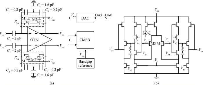
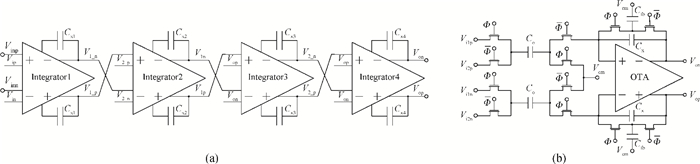
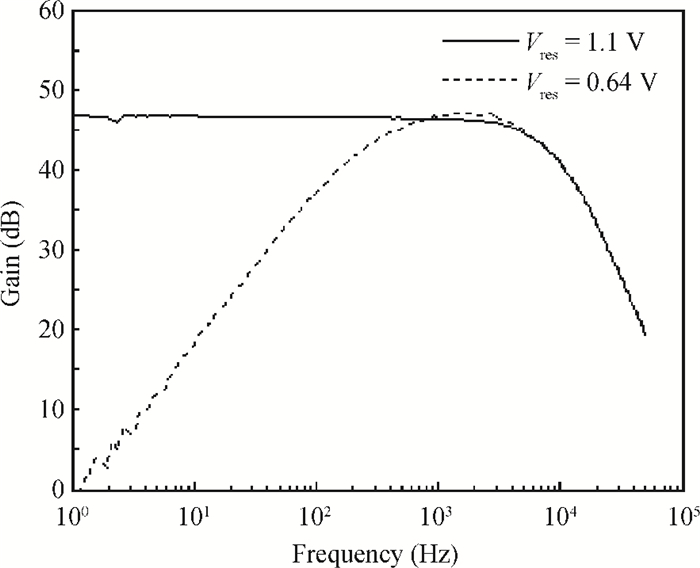
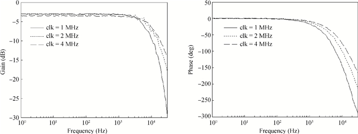
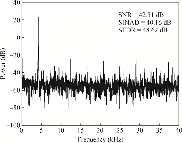
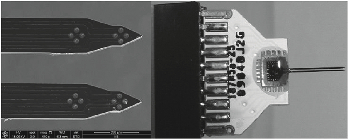
Table 1. Experimental characteristics and comparison.

|
| [1] |
Mountcastle V B. Modality and topographic properties of single neurons of cat's somatic sensory cortex. J Neurophysiol, 1957, 20(4):408 http://jn.physiology.org/content/20/4/408
|
| [2] |
Hubel D H, Wiesel T N. Receptive fields of single neurons in the cat's striate cortex. J Physiol, 1959, 148(3):574 doi: 10.1113/jphysiol.1959.sp006308
|
| [3] |
Pei W, Zhu L, Wang S, et al. Multi-channel micro neural probe fabricated with SOI. Sci China Tech Sci, 2012, 52(5):1187 doi: 10.1007/s11431-008-0272-9?no-access=true
|
| [4] |
Zhao H, Pei W, Chen S, et al. A composite insulation structure for silicon-based planar neuroprobes. Sci China Tech Sci, 2012, 55(9):2436 doi: 10.1007/s11431-012-4856-z
|
| [5] |
Rousche P J, Pellinen D S, Pivin D P, et al. Flexible polyimide-based intracortical electrode arrays with bioactive capability. IEEE Trans Biomed Eng, 2001, 48(3):361 doi: 10.1109/10.914800
|
| [6] |
Li X, Pei W, Tang R, et al. Investigation of flexible electrodes modified by TiN, Pt black and IrOx. Sci China Tech Sci, 2011, 54(9):2305 doi: 10.1007/s11431-011-4436-7
|
| [7] |
Aziz J, Abdelhalim K, Shulyzki R, et al. 256-channel neural recording and delta compression microsystem with 3D electrodes. IEEE J Solid-State Circ, 2009, 44(3):995 doi: 10.1109/JSSC.2008.2010997
|
| [8] |
Harrison R R, Kier R J, Chestek C A, et al. Wireless neural recording with single low-power integrated circuit. IEEE Trans Neural Syst Rehabil Eng, 2009, 17(4):322 doi: 10.1109/TNSRE.2009.2023298
|
| [9] |
Sodagar A, Wise K D, Najafi K. A wireless implantable microsystem for multichannel neural recording. IEEE Trans Microwave Theory Tech, 2009, 57(10):2565 doi: 10.1109/TMTT.2009.2029957
|
| [10] |
Dumortier C, Gosselin B, Sawan M. Wavelet transforms dedicated to compress recorded ENGs from multichannel implants:comparative architectural study. Proc of IEEE Int Symp Circ Syst, 2006:2129 http://ieeexplore.ieee.org/document/1693038/?reload=true&tp=&arnumber=1693038&openedRefinements%3D*%26filter%3DAND(AND(AND(NOT(4283010803)),AND(NOT(4283010803))),AND(NOT(4283010803)))%26pageNumber%3D11%26rowsPerPage%3D100%26queryText%3D(real%20discrete%20wavelet%20transform%20%20rdwt%20de)
|
| [11] |
Horiuchi T, Swindell T, Sander D, et al. A low-power CMOS neural amplifier with amplitude measurements for spike sorting. Proc of IEEE Int Symp Circ Syst, 2004, 4:29 http://ieeexplore.ieee.org/document/1328932/
|
| [12] |
O'Driscoll S, Meng T H, Shenoy K V, et al. Neurons to silicon:implantable prosthesis processor. Proc of IEEE Int Solid-State Circuits Conf, 2006:2248 https://www.infona.pl/resource/bwmeta1.element.ieee-art-000001696287
|
| [13] |
Harrison R R, Charles C. A low-power low-noise CMOS amplifier for neural recording applications. IEEE J Solid-State Circuits, 2003, 38(6):958 doi: 10.1109/JSSC.2003.811979
|
| [14] |
Chae M S, Liu W, Sivaprakasam M. Design optimization for integrated neural recording systems. IEEE J Solid-State Circuits, 2008, 43(9):1931 doi: 10.1109/JSSC.2008.2001877
|
| [15] |
Zhang X. Studies on application specific integrated circuits for neural interfaces. Dissertation for the Doctoral Degree, Beijing:Graduate School of Chinese Academy of Sciences, 2010, 70
|
| [16] |
Zhang X, Pei W, Huang B, et al. A low-noise fully-differential CMOS preamplifier for neural recording applications. Sci China Inf Sci, 2012, 55(2):441 doi: 10.1007/s11432-011-4333-5
|
| [17] |
Olsson R Ⅲ, Buhl D, Sirota A, et al. Band-tunable and multiplexed integrated circuits for simultaneous recording and stimulation with microelectrode arrays. IEEE Trans Biomed Eng, 2005, 52(7):1303 doi: 10.1109/TBME.2005.847540
|
| [18] |
Guillory K S, Normann R A, A 100-channel system for real time detection and storage of extracellular spike waveforms. J Neurosci Methods, 1999, 91(1):21 http://www.sciencedirect.com/science/article/pii/S016502709900076X?via%3Dihub
|
| [19] |
Culurciello E, Andreou A. An 8-bit, 1 mW successive approximation ADC in SOI CMOS. Proc of IEEE Int Symp Circ Syst, 2003, 1:301 http://ieeexplore.ieee.org/document/1205560/authors
|
| [20] |
Gosselin B, Ayoub A E, Roy J, et al. A mixed-signal multichip neural recording interface with bandwidth reduction. IEEE Trans Biomed Circ and Syst, 2009, 3(3):129 doi: 10.1109/TBCAS.2009.2013718
|
| [21] |
Kmon P, Zoladz M, Grybos P, et al. Design and measurements of 64-channel ASIC for neural signal recording. Proc of 31st Int Conf IEEE Eng Med Biol Soc, 2009:528 http://ieeexplore.ieee.org/document/5333629/
|
| [22] |
Shahrokhi F, Abdelhalim K, Serletis D, et al. The 128-channel fully differential digital integrated neural recording and stimulation interface. IEEE Trans Biomed Circ and Syst, 2010, 4(3):149 doi: 10.1109/TBCAS.2010.2041350
|


Article views: 3233 Times PDF downloads: 26 Times Cited by: 0 Times
Received: 05 March 2013 Revised: 22 March 2013 Online: Published: 01 October 2013
| Citation: |
Yun Gui, Xu Zhang, Yuan Wang, Ming Liu, Weihua Pei, Kai Liang, Suibiao Huang, Bin Li, Hongda Chen. A multi-channel fully differential programmable integrated circuit for neural recording application[J]. Journal of Semiconductors, 2013, 34(10): 105009. doi: 10.1088/1674-4926/34/10/105009
****
Y Gui, X Zhang, Y Wang, M Liu, W H Pei, K Liang, S B Huang, B Li, H D Chen. A multi-channel fully differential programmable integrated circuit for neural recording application[J]. J. Semicond., 2013, 34(10): 105009. doi: 10.1088/1674-4926/34/10/105009.

|
| [1] |
Mountcastle V B. Modality and topographic properties of single neurons of cat's somatic sensory cortex. J Neurophysiol, 1957, 20(4):408 http://jn.physiology.org/content/20/4/408
|
| [2] |
Hubel D H, Wiesel T N. Receptive fields of single neurons in the cat's striate cortex. J Physiol, 1959, 148(3):574 doi: 10.1113/jphysiol.1959.sp006308
|
| [3] |
Pei W, Zhu L, Wang S, et al. Multi-channel micro neural probe fabricated with SOI. Sci China Tech Sci, 2012, 52(5):1187 doi: 10.1007/s11431-008-0272-9?no-access=true
|
| [4] |
Zhao H, Pei W, Chen S, et al. A composite insulation structure for silicon-based planar neuroprobes. Sci China Tech Sci, 2012, 55(9):2436 doi: 10.1007/s11431-012-4856-z
|
| [5] |
Rousche P J, Pellinen D S, Pivin D P, et al. Flexible polyimide-based intracortical electrode arrays with bioactive capability. IEEE Trans Biomed Eng, 2001, 48(3):361 doi: 10.1109/10.914800
|
| [6] |
Li X, Pei W, Tang R, et al. Investigation of flexible electrodes modified by TiN, Pt black and IrOx. Sci China Tech Sci, 2011, 54(9):2305 doi: 10.1007/s11431-011-4436-7
|
| [7] |
Aziz J, Abdelhalim K, Shulyzki R, et al. 256-channel neural recording and delta compression microsystem with 3D electrodes. IEEE J Solid-State Circ, 2009, 44(3):995 doi: 10.1109/JSSC.2008.2010997
|
| [8] |
Harrison R R, Kier R J, Chestek C A, et al. Wireless neural recording with single low-power integrated circuit. IEEE Trans Neural Syst Rehabil Eng, 2009, 17(4):322 doi: 10.1109/TNSRE.2009.2023298
|
| [9] |
Sodagar A, Wise K D, Najafi K. A wireless implantable microsystem for multichannel neural recording. IEEE Trans Microwave Theory Tech, 2009, 57(10):2565 doi: 10.1109/TMTT.2009.2029957
|
| [10] |
Dumortier C, Gosselin B, Sawan M. Wavelet transforms dedicated to compress recorded ENGs from multichannel implants:comparative architectural study. Proc of IEEE Int Symp Circ Syst, 2006:2129 http://ieeexplore.ieee.org/document/1693038/?reload=true&tp=&arnumber=1693038&openedRefinements%3D*%26filter%3DAND(AND(AND(NOT(4283010803)),AND(NOT(4283010803))),AND(NOT(4283010803)))%26pageNumber%3D11%26rowsPerPage%3D100%26queryText%3D(real%20discrete%20wavelet%20transform%20%20rdwt%20de)
|
| [11] |
Horiuchi T, Swindell T, Sander D, et al. A low-power CMOS neural amplifier with amplitude measurements for spike sorting. Proc of IEEE Int Symp Circ Syst, 2004, 4:29 http://ieeexplore.ieee.org/document/1328932/
|
| [12] |
O'Driscoll S, Meng T H, Shenoy K V, et al. Neurons to silicon:implantable prosthesis processor. Proc of IEEE Int Solid-State Circuits Conf, 2006:2248 https://www.infona.pl/resource/bwmeta1.element.ieee-art-000001696287
|
| [13] |
Harrison R R, Charles C. A low-power low-noise CMOS amplifier for neural recording applications. IEEE J Solid-State Circuits, 2003, 38(6):958 doi: 10.1109/JSSC.2003.811979
|
| [14] |
Chae M S, Liu W, Sivaprakasam M. Design optimization for integrated neural recording systems. IEEE J Solid-State Circuits, 2008, 43(9):1931 doi: 10.1109/JSSC.2008.2001877
|
| [15] |
Zhang X. Studies on application specific integrated circuits for neural interfaces. Dissertation for the Doctoral Degree, Beijing:Graduate School of Chinese Academy of Sciences, 2010, 70
|
| [16] |
Zhang X, Pei W, Huang B, et al. A low-noise fully-differential CMOS preamplifier for neural recording applications. Sci China Inf Sci, 2012, 55(2):441 doi: 10.1007/s11432-011-4333-5
|
| [17] |
Olsson R Ⅲ, Buhl D, Sirota A, et al. Band-tunable and multiplexed integrated circuits for simultaneous recording and stimulation with microelectrode arrays. IEEE Trans Biomed Eng, 2005, 52(7):1303 doi: 10.1109/TBME.2005.847540
|
| [18] |
Guillory K S, Normann R A, A 100-channel system for real time detection and storage of extracellular spike waveforms. J Neurosci Methods, 1999, 91(1):21 http://www.sciencedirect.com/science/article/pii/S016502709900076X?via%3Dihub
|
| [19] |
Culurciello E, Andreou A. An 8-bit, 1 mW successive approximation ADC in SOI CMOS. Proc of IEEE Int Symp Circ Syst, 2003, 1:301 http://ieeexplore.ieee.org/document/1205560/authors
|
| [20] |
Gosselin B, Ayoub A E, Roy J, et al. A mixed-signal multichip neural recording interface with bandwidth reduction. IEEE Trans Biomed Circ and Syst, 2009, 3(3):129 doi: 10.1109/TBCAS.2009.2013718
|
| [21] |
Kmon P, Zoladz M, Grybos P, et al. Design and measurements of 64-channel ASIC for neural signal recording. Proc of 31st Int Conf IEEE Eng Med Biol Soc, 2009:528 http://ieeexplore.ieee.org/document/5333629/
|
| [22] |
Shahrokhi F, Abdelhalim K, Serletis D, et al. The 128-channel fully differential digital integrated neural recording and stimulation interface. IEEE Trans Biomed Circ and Syst, 2010, 4(3):149 doi: 10.1109/TBCAS.2010.2041350
|

 WeChat ID
Journal of Semiconductors © 2017 All Rights Reserved 京ICP备05085259号-2

 DownLoad: