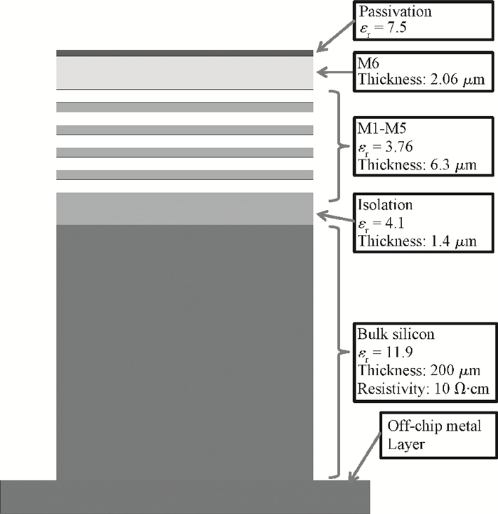
Fig. 1.
Cross section of the 0.18 $\mu $ m CMOS technology after the back grinding process.
SEMICONDUCTOR INTEGRATED CIRCUITS
Xiangyu Meng1, , Baoyong Chi1, Haikun Jia1, Lixue Kuang1, Wen Jia2 and Zhihua Wang1
Corresponding author: Meng Xiangyu, mengxy11@mails.tsinghua.edu.cn
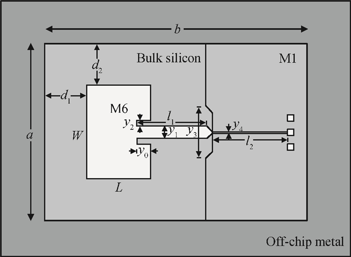
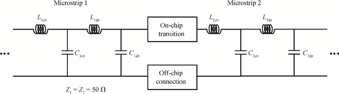
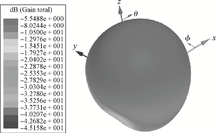
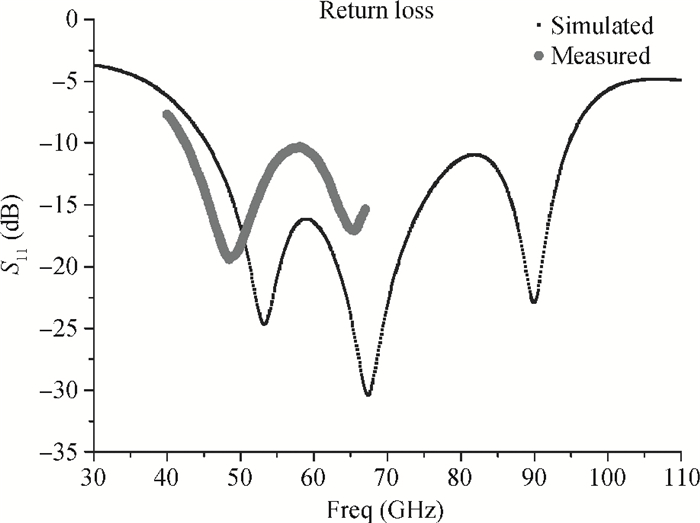
Abstract: A wideband on-chip millimeter-wave patch antenna in 0.18 μm CMOS with a low-resistivity (10 Ω· cm) silicon substrate is presented. The wideband is achieved by reducing the Q factor and exciting the high-order radiation modes with size optimization. The antenna uses an on-chip top layer metal as the patch and a probe station as the ground plane. The on-chip ground plane is connected to the probe station using the inner connection structure of the probe station for better performance. The simulated S11 is less than -10 dB over 46-95 GHz, which is well matched with the measured results over the available 40-67 GHz frequency range from our measurement equipment. A maximum gain of -5.55 dBi with 4% radiation efficiency at a 60 GHz point is also achieved based on Ansoft HFSS simulation. Compared with the current state-of-the-art devices, the presented antenna achieves a wider bandwidth and could be used in wideband millimeter-wave communication and image applications.
Keywords: on-chip antenna, patch antenna, wideband antenna, millimeter-wave
| [1] |
Carver K R, Mink J W. Microstrip antenna technology. IEEE Trans Antennas Propagation, 1981, 29(1):2 doi: 10.1109/TAP.1981.1142523
|
| [2] |
Milligan T A. Modern antenna design. 2nd ed. John Wiley & Sons, Inc, 2005
|
| [3] |
Hsu S S, Wei K C, Hsu C Y, et al. A 60-GHz millimeter-wave CPW-fed yagi antenna fabricated by using 0.18μm CMOS technology. IEEE Electron Device Lett, 2008, 29(6):625
|
| [4] |
Guo P J, Chuang H R. A 60-GHz millimeter-wave CMOS RFIC-on-chip meander-line planar inverted-f antenna for WPAN applications. Antennas and Propagation society International Symposium, 2008:1 http://ieeexplore.ieee.org/document/4619464/
|
| [5] |
Lin C C, Hsu S S, Hsu C Y, et al. A 60-GHz millimeter-wave CMOS RFIC-on-chip triangular monopole antenna for WPAN applications. IEEE Antennas Propag Soc Int Symp, 2007:2522 http://ieeexplore.ieee.org/document/4396047/
|
| [6] |
Huang K K, Wentzloff D D. 60 GHz on-chip patch antenna integrated in a 0.13-μm CMOS technology. Ultra-Wideband (ICUWB), 2010:1
|
| [7] |
Han R, Zhang Y, Kim Y. 280 GHz and 860 GHz image sensors using Schottky-barrier diodes in 0.13μm digital CMOS. Solid-State Circuits Conference Digest of Technical Papers (ISSCC), 2012:254
|
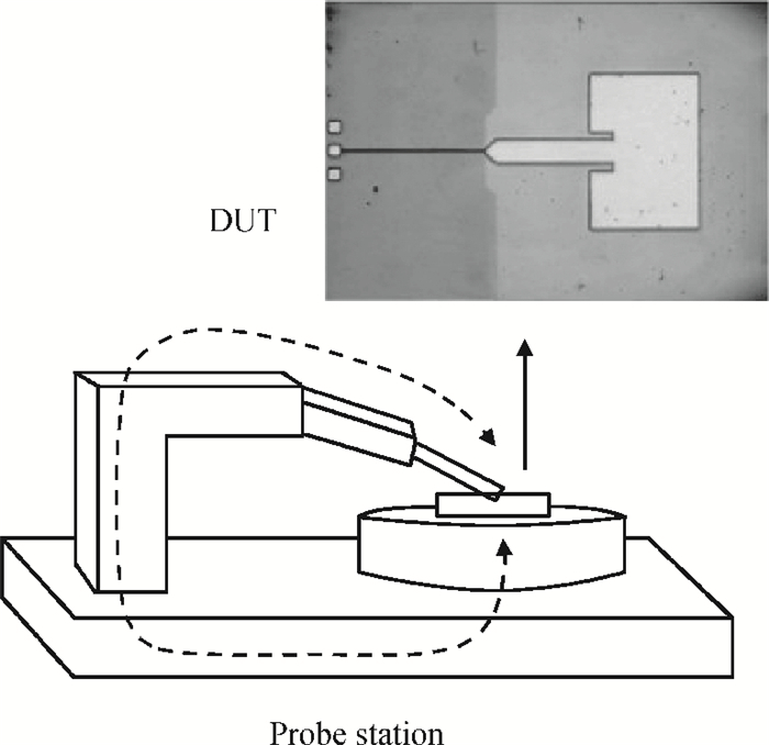
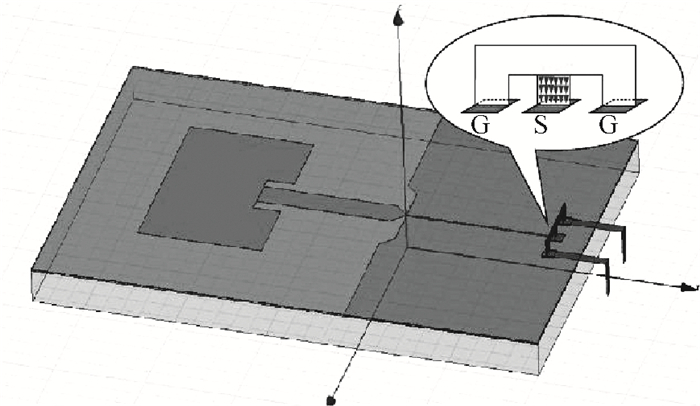
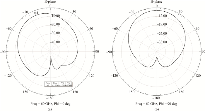
Table 1. The parameters of the presented on-chip patch antenna.

|
Table 2. Performance summary and comparison with the state-of-the-arts devices.

|
| [1] |
Carver K R, Mink J W. Microstrip antenna technology. IEEE Trans Antennas Propagation, 1981, 29(1):2 doi: 10.1109/TAP.1981.1142523
|
| [2] |
Milligan T A. Modern antenna design. 2nd ed. John Wiley & Sons, Inc, 2005
|
| [3] |
Hsu S S, Wei K C, Hsu C Y, et al. A 60-GHz millimeter-wave CPW-fed yagi antenna fabricated by using 0.18μm CMOS technology. IEEE Electron Device Lett, 2008, 29(6):625
|
| [4] |
Guo P J, Chuang H R. A 60-GHz millimeter-wave CMOS RFIC-on-chip meander-line planar inverted-f antenna for WPAN applications. Antennas and Propagation society International Symposium, 2008:1 http://ieeexplore.ieee.org/document/4619464/
|
| [5] |
Lin C C, Hsu S S, Hsu C Y, et al. A 60-GHz millimeter-wave CMOS RFIC-on-chip triangular monopole antenna for WPAN applications. IEEE Antennas Propag Soc Int Symp, 2007:2522 http://ieeexplore.ieee.org/document/4396047/
|
| [6] |
Huang K K, Wentzloff D D. 60 GHz on-chip patch antenna integrated in a 0.13-μm CMOS technology. Ultra-Wideband (ICUWB), 2010:1
|
| [7] |
Han R, Zhang Y, Kim Y. 280 GHz and 860 GHz image sensors using Schottky-barrier diodes in 0.13μm digital CMOS. Solid-State Circuits Conference Digest of Technical Papers (ISSCC), 2012:254
|


Article views: 3380 Times PDF downloads: 24 Times Cited by: 0 Times
Received: 21 March 2013 Revised: 19 April 2013 Online: Published: 01 October 2013
| Citation: |
Xiangyu Meng, Baoyong Chi, Haikun Jia, Lixue Kuang, Wen Jia, Zhihua Wang. A wideband on-chip millimeter-wave patch antenna in 0.18 μm CMOS[J]. Journal of Semiconductors, 2013, 34(10): 105010. doi: 10.1088/1674-4926/34/10/105010
****
X Y Meng, B Y Chi, H K Jia, L X Kuang, W Jia, Z H Wang. A wideband on-chip millimeter-wave patch antenna in 0.18 μm CMOS[J]. J. Semicond., 2013, 34(10): 105010. doi: 10.1088/1674-4926/34/10/105010.

|
| [1] |
Carver K R, Mink J W. Microstrip antenna technology. IEEE Trans Antennas Propagation, 1981, 29(1):2 doi: 10.1109/TAP.1981.1142523
|
| [2] |
Milligan T A. Modern antenna design. 2nd ed. John Wiley & Sons, Inc, 2005
|
| [3] |
Hsu S S, Wei K C, Hsu C Y, et al. A 60-GHz millimeter-wave CPW-fed yagi antenna fabricated by using 0.18μm CMOS technology. IEEE Electron Device Lett, 2008, 29(6):625
|
| [4] |
Guo P J, Chuang H R. A 60-GHz millimeter-wave CMOS RFIC-on-chip meander-line planar inverted-f antenna for WPAN applications. Antennas and Propagation society International Symposium, 2008:1 http://ieeexplore.ieee.org/document/4619464/
|
| [5] |
Lin C C, Hsu S S, Hsu C Y, et al. A 60-GHz millimeter-wave CMOS RFIC-on-chip triangular monopole antenna for WPAN applications. IEEE Antennas Propag Soc Int Symp, 2007:2522 http://ieeexplore.ieee.org/document/4396047/
|
| [6] |
Huang K K, Wentzloff D D. 60 GHz on-chip patch antenna integrated in a 0.13-μm CMOS technology. Ultra-Wideband (ICUWB), 2010:1
|
| [7] |
Han R, Zhang Y, Kim Y. 280 GHz and 860 GHz image sensors using Schottky-barrier diodes in 0.13μm digital CMOS. Solid-State Circuits Conference Digest of Technical Papers (ISSCC), 2012:254
|

 WeChat ID
Journal of Semiconductors © 2017 All Rights Reserved 京ICP备05085259号-2

 DownLoad: