


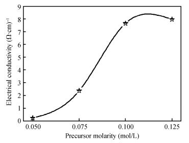
Fig. 1.
Variation of electrical conductivity of ZnO thin films as a function of spray concentration.
SEMICONDUCTOR MATERIALS
Said Benramache1, Okba Belahssen1, 2, Abderrazak Guettaf3 and Ali Arif3
Abstract: ZnO thin films were deposited using the simple, flexible and cost-effective spray ultrasonic technique at different precursor molarities values. The films were deposited on a glass substrate at 350℃. This paper is to present a new approach to the description of correlation between electrical conductivity and optical gap energy with precursor molarity of ZnO thin films. The ZnO films exhibit higher electrical n-type semiconductors, whose band gap energy increased from 3.08 to 3.37 eV with an increasing of precursor molarity of 0.05 to 0.1 M. The maximum value of electrical conductivity of the films is 7.96 (Ω·cm)-1 obtained in the ZnO thin film for precursor molarity 0.125 M. The correlation between the electrical and the optical properties with the precursor molarity suggests that the electrical conductivity of the films is predominantly influenced by the band gap energy and the precursor molarity. The measurement of the electrical conductivity of the films with correlation is equal to the experimental with the error is about 1% in the higher conductivity.
Keywords: ZnO, thin films, correlation, electrical conductivity, ultrasonic spray technique
| [1] |
Zhang Y, Wu C, Zheng Y, et al. Synthesis and efficient field emission characteristics of patterned ZnO nanowires. Journal of Semiconductors, 2012, 33(2):023001 doi: 10.1088/1674-4926/33/2/023001
|
| [2] |
Benramache S, Benhaoua B, Chabane F, et al. Effect of the dip-coating speed on the structural and optical properties of ZnO thin films. International Journal of Science and Engineering Investigations, 2012, 1(3):28 https://www.scientific.net/JERA.31.29
|
| [3] |
Zhang Z, Bao C, Yao W, et al. Influence of deposition temperature on the crystallinity of Al-doped ZnO thin films at glass substrates prepared by RF magnetron sputtering method. Superlattices and Microstructures, 2011, 49(6):644 doi: 10.1016/j.spmi.2011.04.002
|
| [4] |
Zhu X, Wu H, Wang S, et al. Optical and electrical properties of N-doped ZnO and fabrication of thin-film transistors. Journal of Semiconductors, 2009, 30(3):033001 doi: 10.1088/1674-4926/30/3/033001
|
| [5] |
Zhang H, Liu H, Lei C, et al. Low-temperature deposition of transparent conducting Mn-W co-doped ZnO thin films. Journal of Semiconductors, 2010, 31(8):083005 doi: 10.1088/1674-4926/31/8/083005
|
| [6] |
Ben Ayadi Z, El Mir L, Djessas K, et al. Effect of the annealing temperature on transparency and conductivity of ZnO:Al thin films. Thin Solid Films, 2009, 517(22):6305
|
| [7] |
Nunes P, Fortunato E, Martins R. Effect of different dopants on the properties of ZnO thin films. International Journal Inorganic Materials, 2001, 3(8):1125 doi: 10.1016/S1466-6049(01)00113-1
|
| [8] |
Gupta B, Jain A, Mehra R M. Development and characterization of sol-gel derived Al doped ZnO/p-Si photodiode. J Mater Sci Technol, 2010, 26(3):223 doi: 10.1016/S1005-0302(10)60037-0
|
| [9] |
Bahs Z B, Oral A Y. Effects of Mn and Cu doping on the microstructures and optical properties of sol-gel derived ZnO thin films. Opt Mater, 2007, 29(3):672 doi: 10.1186/2193-8865-3-54
|
| [10] |
Yan X, Hu D, Li H, et al. Nanostructure and optical properties of M doped ZnO (M=Ni, Mn) thin films prepared by sol-gel process. Physica B, 2011, 406(20):3956 doi: 10.1016/j.physb.2011.07.037
|
| [11] |
Singhal S, Chawla A K, Gupta H O, et al. Influence of cobalt doping on the physical properties of Zn0.9Cd0.1S nanoparticles. Nanoscale Research Letters, 2009, 5(2):323 http://www.oalib.com/paper/2529708
|
| [12] |
Wang B, Callahan M J, Chunchuan X U, et al. Hydrothermal growth and characterization of indium-doped-conducting ZnO crystals. J Cryst Growth, 2007, 304(1):73 doi: 10.1016/j.jcrysgro.2007.01.047
|
| [13] |
Kang S J, Joung Y H, Shin H H, et al. Effect of substrate temperature on structural, optical and electrical properties of ZnO thin films deposited by pulsed laser deposition. J Mater Sci Mater Electron, 2008, 19(11):1073 doi: 10.1007/s10854-007-9469-0
|
| [14] |
Vernardou D, Kenanakis G, Couris S, et al. The effect of growth time on the morphology of ZnO structures deposited on Si (100) by the aqueous chemical growth technique. J Cryst Growth, 2007, 308(2):105
|
| [15] |
Gahtar A, Benramache S, Benhaoua B, et al. Preparation of transparent conducting ZnO:Al films on glass substrates by ultrasonic spray technique. Journal of Semiconductors, 2013, 34(7):073001 doi: 10.1088/1674-4926/34/7/073001
|
| [16] |
Ivill M, Pearton S J, Norton D P, et al. Magnetization dependence on electron density in epitaxial ZnO thin films codoped with Mn and Sn. J Appl Phys, 2005, 97(5):53904 doi: 10.1063/1.1856225
|
| [17] |
Vollmann W, Berger W, Hamann C, et al. Relations between the morphology and conductivity of thin films of tetrathiofulvalin-iumtetracyanoquinodimethane. Thin Solid Films, 1984, 111(1):7 doi: 10.1016/0040-6090(84)90344-4
|
| [18] |
Asadov A, Gao W, Li Z, et al. Correlation between structural and electrical properties of ZnO thin films. Thin Solid Films, 2005, 476(1):201 doi: 10.1016/j.tsf.2004.09.038
|
| [19] |
Vimalkumar T V, Poornima N, Jinesh B K, et al. On single doping and doping of spray pyrolysed ZnO films, structural and electrical optical characterization. Appl Surf Sci, 2011, 257(20):8333
|
| [20] |
Benramache S, Benhaoua B, Chabane F. Effect of substrate temperature on the stability of transparent conducting cobalt doped ZnO thin films. Journal of Semiconductors, 2012, 33(9):093001 doi: 10.1088/1674-4926/33/9/093001
|
| [21] |
Ton-That C, Foley M, Phillips M R, et al. Correlation between the structural and optical properties of Mn-doped ZnO nanoparticles. Journal of Alloys and Compounds, 2012, 522(1):114 http://www.doc88.com/p-6721229377937.html
|
| [22] |
Kappertz O, Drese R, Wuttig M. Correlation between structure, stress and deposition parameters in direct current sputtered zinc oxide films. J Vac Sci Technol A, 2002, 20(6):2084 doi: 10.1116/1.1517997
|
| [23] |
Tudose I V, Horvath P, Suchea M, et al. Correlation of ZnO thin film surface properties with conductivity. Appl Phys A, 2007, 89(1):57 doi: 10.1007/s00339-007-4036-3
|
| [24] |
Joshi B, Ghosh S, Srivastava P, et al. Correlation between electrical transport, microstructure and room temperature ferromagnetism in 200 keV Ni2+ ion implanted zinc oxide (ZnO) thin films. Appl Phys A, 2012, 107(2):393 doi: 10.1007%2Fs00339-012-6785-x.pdf
|
| [25] |
Wang S D., Miyadera T, Minari T, et al. Correlation between grain size and device parameters in pentacene thin film transistors. Appl Phys Lett, 2008, 93(4):043311 doi: 10.1063/1.2967193
|
| [26] |
Minami T, Nanto H, Takata S. Correlation between film quality and photoluminescence in sputtered ZnO thin films. J Mater Sci, 1982, 17(5):1364 doi: 10.1007/BF00752247
|
| [27] |
Zhu J J, Vines L, Aaltonen T, et al. Correlation between nitrogen and carbon incorporation into MOVPE ZnO at various oxidizing conditions. Microelectron J, 2009, 40(2):232 doi: 10.1016/j.mejo.2008.07.042
|
| [28] |
Nakanishi Y, Kato K, Omoto H, et al. Correlation between microstructure and salt-water durability of Ag thin films deposited by magnetron sputtering. Thin Solid Films, 2013, 532(1):141 http://adsabs.harvard.edu/abs/2013TSF...532..141N
|
| [29] |
Ajimsha R S, Das, A K, Singh B N, et al. Correlation between electrical and optical properties of Cr:ZnO thin films grown by pulsed laser deposition. Physica B, 2011, 406:4578 doi: 10.1016/j.physb.2011.09.024
|
| [30] |
Zak A K, Abd Majid W H, Abrishami M E, et al. X-ray analysis of ZnO nanoparticles by Williamson-Hall and size-strain plotmethods. Solid State Sci, 2011, 13(2):251 http://adsabs.harvard.edu/abs/2011SSSci..13..251K
|
| [31] |
Benramache S, Benhaoua B. Influence of annealing temperature on structural and optical properties of ZnO:In thin films prepared by ultrasonic spray technique. Superlattices and Microstructures, 2012, 52(6):1062 doi: 10.1016/j.spmi.2012.08.006
|
| [32] |
Benramache S, Benhaoua B. Influence of substrate temperature and Cobalt concentration on structural and optical properties of ZnO thin films prepared by ultrasonic spray technique, Superlattices and Microstructures, 2012, 52(4):807 http://www.nsfc.gov.cn/Portals/0/fj/fj20170118_03.xls
|
| [33] |
Li Y, Gong J, McCune M, et al. I-V characteristics of the p-n junction between vertically aligned ZnO nanorods and polyaniline thin film, Synthetic Metals, 2010, 160(3):498 doi: 10.1007/s10904-016-0333-7
|
| [34] |
Benramache S, Chabane F, Benhaoua B, et al. Influence of growth time on crystalline structure, conductivity and optical properties of ZnO thin films. Journal of Semiconductors, 2013, 34(2):023001 doi: 10.1088/1674-4926/34/2/023001
|
| [35] |
Benramache S, Benhaoua B, Chabane F, et al. A comparative study on the nanocrystalline ZnO thin films prepared by ultrasonic spray and sol-gel method. Optik, 2012.http://dx.doi.org/10.1016/j.ijleo.2012.10.001 http://www.doc88.com/p-9169554173002.html
|
| [36] |
Samanta K, Bhattacharya P, Duque J G S, et al. Optical and magnetic properties of Zn0.9-xCo0.1O:Alx thin films. Solid State Commun, 2008, 147(7/8):305
|
| [37] |
Senadi m E, Eker S, Kavak H, et al. Optical and structural parameters of the ZnO thin film grown by pulsed filtered cathodic vacuum arc deposition. Solid State Commun, 2006, 139(9):479 doi: 10.1016/j.ssc.2006.07.001
|
| [38] |
Subramanian M, Tanemura M, Hihara T, et al. Magnetic anisotropy in nanocrystalline Co-doped ZnO thin films. Chem Phys Lett, 2010, 487(1):97
|
| [39] |
Gahtar A, Benramache S, Benhaoua B, et al. Preparation of transparent conducting ZnO:Al films on glass substrates by ultrasonic spray technique. Journal of Semiconductors, 2013, 34(7):033001 http://www.jos.ac.cn/bdtxbcn/ch/reader/view_abstract.aspx?file_no=12101001&flag=1
|
| [40] |
Daranfed W, Aida M S, Hafdallah A, et al. Substrate temperature influence on ZnS thin films prepared by ultrasonic spray. Thin Solid Films, 2009, 518(3):1080
|
| [41] |
Benramache S, Benhaoua B, Khechai N, et al. Elaboration and characterisation of ZnO thin films. Matériaux & Techniques, 2012, 100(6/7): 573 http://www.wenkuxiazai.com/doc/2e70a31d10a6f524ccbf85a5.html
|
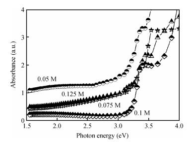
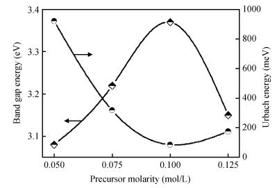
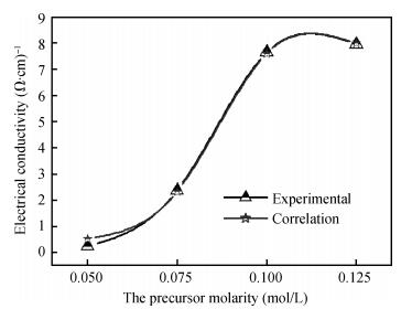
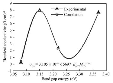
Table 1.
Optical band gap energy

|
Table 2.
The experimental electrical conductivity

|
| [1] |
Zhang Y, Wu C, Zheng Y, et al. Synthesis and efficient field emission characteristics of patterned ZnO nanowires. Journal of Semiconductors, 2012, 33(2):023001 doi: 10.1088/1674-4926/33/2/023001
|
| [2] |
Benramache S, Benhaoua B, Chabane F, et al. Effect of the dip-coating speed on the structural and optical properties of ZnO thin films. International Journal of Science and Engineering Investigations, 2012, 1(3):28 https://www.scientific.net/JERA.31.29
|
| [3] |
Zhang Z, Bao C, Yao W, et al. Influence of deposition temperature on the crystallinity of Al-doped ZnO thin films at glass substrates prepared by RF magnetron sputtering method. Superlattices and Microstructures, 2011, 49(6):644 doi: 10.1016/j.spmi.2011.04.002
|
| [4] |
Zhu X, Wu H, Wang S, et al. Optical and electrical properties of N-doped ZnO and fabrication of thin-film transistors. Journal of Semiconductors, 2009, 30(3):033001 doi: 10.1088/1674-4926/30/3/033001
|
| [5] |
Zhang H, Liu H, Lei C, et al. Low-temperature deposition of transparent conducting Mn-W co-doped ZnO thin films. Journal of Semiconductors, 2010, 31(8):083005 doi: 10.1088/1674-4926/31/8/083005
|
| [6] |
Ben Ayadi Z, El Mir L, Djessas K, et al. Effect of the annealing temperature on transparency and conductivity of ZnO:Al thin films. Thin Solid Films, 2009, 517(22):6305
|
| [7] |
Nunes P, Fortunato E, Martins R. Effect of different dopants on the properties of ZnO thin films. International Journal Inorganic Materials, 2001, 3(8):1125 doi: 10.1016/S1466-6049(01)00113-1
|
| [8] |
Gupta B, Jain A, Mehra R M. Development and characterization of sol-gel derived Al doped ZnO/p-Si photodiode. J Mater Sci Technol, 2010, 26(3):223 doi: 10.1016/S1005-0302(10)60037-0
|
| [9] |
Bahs Z B, Oral A Y. Effects of Mn and Cu doping on the microstructures and optical properties of sol-gel derived ZnO thin films. Opt Mater, 2007, 29(3):672 doi: 10.1186/2193-8865-3-54
|
| [10] |
Yan X, Hu D, Li H, et al. Nanostructure and optical properties of M doped ZnO (M=Ni, Mn) thin films prepared by sol-gel process. Physica B, 2011, 406(20):3956 doi: 10.1016/j.physb.2011.07.037
|
| [11] |
Singhal S, Chawla A K, Gupta H O, et al. Influence of cobalt doping on the physical properties of Zn0.9Cd0.1S nanoparticles. Nanoscale Research Letters, 2009, 5(2):323 http://www.oalib.com/paper/2529708
|
| [12] |
Wang B, Callahan M J, Chunchuan X U, et al. Hydrothermal growth and characterization of indium-doped-conducting ZnO crystals. J Cryst Growth, 2007, 304(1):73 doi: 10.1016/j.jcrysgro.2007.01.047
|
| [13] |
Kang S J, Joung Y H, Shin H H, et al. Effect of substrate temperature on structural, optical and electrical properties of ZnO thin films deposited by pulsed laser deposition. J Mater Sci Mater Electron, 2008, 19(11):1073 doi: 10.1007/s10854-007-9469-0
|
| [14] |
Vernardou D, Kenanakis G, Couris S, et al. The effect of growth time on the morphology of ZnO structures deposited on Si (100) by the aqueous chemical growth technique. J Cryst Growth, 2007, 308(2):105
|
| [15] |
Gahtar A, Benramache S, Benhaoua B, et al. Preparation of transparent conducting ZnO:Al films on glass substrates by ultrasonic spray technique. Journal of Semiconductors, 2013, 34(7):073001 doi: 10.1088/1674-4926/34/7/073001
|
| [16] |
Ivill M, Pearton S J, Norton D P, et al. Magnetization dependence on electron density in epitaxial ZnO thin films codoped with Mn and Sn. J Appl Phys, 2005, 97(5):53904 doi: 10.1063/1.1856225
|
| [17] |
Vollmann W, Berger W, Hamann C, et al. Relations between the morphology and conductivity of thin films of tetrathiofulvalin-iumtetracyanoquinodimethane. Thin Solid Films, 1984, 111(1):7 doi: 10.1016/0040-6090(84)90344-4
|
| [18] |
Asadov A, Gao W, Li Z, et al. Correlation between structural and electrical properties of ZnO thin films. Thin Solid Films, 2005, 476(1):201 doi: 10.1016/j.tsf.2004.09.038
|
| [19] |
Vimalkumar T V, Poornima N, Jinesh B K, et al. On single doping and doping of spray pyrolysed ZnO films, structural and electrical optical characterization. Appl Surf Sci, 2011, 257(20):8333
|
| [20] |
Benramache S, Benhaoua B, Chabane F. Effect of substrate temperature on the stability of transparent conducting cobalt doped ZnO thin films. Journal of Semiconductors, 2012, 33(9):093001 doi: 10.1088/1674-4926/33/9/093001
|
| [21] |
Ton-That C, Foley M, Phillips M R, et al. Correlation between the structural and optical properties of Mn-doped ZnO nanoparticles. Journal of Alloys and Compounds, 2012, 522(1):114 http://www.doc88.com/p-6721229377937.html
|
| [22] |
Kappertz O, Drese R, Wuttig M. Correlation between structure, stress and deposition parameters in direct current sputtered zinc oxide films. J Vac Sci Technol A, 2002, 20(6):2084 doi: 10.1116/1.1517997
|
| [23] |
Tudose I V, Horvath P, Suchea M, et al. Correlation of ZnO thin film surface properties with conductivity. Appl Phys A, 2007, 89(1):57 doi: 10.1007/s00339-007-4036-3
|
| [24] |
Joshi B, Ghosh S, Srivastava P, et al. Correlation between electrical transport, microstructure and room temperature ferromagnetism in 200 keV Ni2+ ion implanted zinc oxide (ZnO) thin films. Appl Phys A, 2012, 107(2):393 doi: 10.1007%2Fs00339-012-6785-x.pdf
|
| [25] |
Wang S D., Miyadera T, Minari T, et al. Correlation between grain size and device parameters in pentacene thin film transistors. Appl Phys Lett, 2008, 93(4):043311 doi: 10.1063/1.2967193
|
| [26] |
Minami T, Nanto H, Takata S. Correlation between film quality and photoluminescence in sputtered ZnO thin films. J Mater Sci, 1982, 17(5):1364 doi: 10.1007/BF00752247
|
| [27] |
Zhu J J, Vines L, Aaltonen T, et al. Correlation between nitrogen and carbon incorporation into MOVPE ZnO at various oxidizing conditions. Microelectron J, 2009, 40(2):232 doi: 10.1016/j.mejo.2008.07.042
|
| [28] |
Nakanishi Y, Kato K, Omoto H, et al. Correlation between microstructure and salt-water durability of Ag thin films deposited by magnetron sputtering. Thin Solid Films, 2013, 532(1):141 http://adsabs.harvard.edu/abs/2013TSF...532..141N
|
| [29] |
Ajimsha R S, Das, A K, Singh B N, et al. Correlation between electrical and optical properties of Cr:ZnO thin films grown by pulsed laser deposition. Physica B, 2011, 406:4578 doi: 10.1016/j.physb.2011.09.024
|
| [30] |
Zak A K, Abd Majid W H, Abrishami M E, et al. X-ray analysis of ZnO nanoparticles by Williamson-Hall and size-strain plotmethods. Solid State Sci, 2011, 13(2):251 http://adsabs.harvard.edu/abs/2011SSSci..13..251K
|
| [31] |
Benramache S, Benhaoua B. Influence of annealing temperature on structural and optical properties of ZnO:In thin films prepared by ultrasonic spray technique. Superlattices and Microstructures, 2012, 52(6):1062 doi: 10.1016/j.spmi.2012.08.006
|
| [32] |
Benramache S, Benhaoua B. Influence of substrate temperature and Cobalt concentration on structural and optical properties of ZnO thin films prepared by ultrasonic spray technique, Superlattices and Microstructures, 2012, 52(4):807 http://www.nsfc.gov.cn/Portals/0/fj/fj20170118_03.xls
|
| [33] |
Li Y, Gong J, McCune M, et al. I-V characteristics of the p-n junction between vertically aligned ZnO nanorods and polyaniline thin film, Synthetic Metals, 2010, 160(3):498 doi: 10.1007/s10904-016-0333-7
|
| [34] |
Benramache S, Chabane F, Benhaoua B, et al. Influence of growth time on crystalline structure, conductivity and optical properties of ZnO thin films. Journal of Semiconductors, 2013, 34(2):023001 doi: 10.1088/1674-4926/34/2/023001
|
| [35] |
Benramache S, Benhaoua B, Chabane F, et al. A comparative study on the nanocrystalline ZnO thin films prepared by ultrasonic spray and sol-gel method. Optik, 2012.http://dx.doi.org/10.1016/j.ijleo.2012.10.001 http://www.doc88.com/p-9169554173002.html
|
| [36] |
Samanta K, Bhattacharya P, Duque J G S, et al. Optical and magnetic properties of Zn0.9-xCo0.1O:Alx thin films. Solid State Commun, 2008, 147(7/8):305
|
| [37] |
Senadi m E, Eker S, Kavak H, et al. Optical and structural parameters of the ZnO thin film grown by pulsed filtered cathodic vacuum arc deposition. Solid State Commun, 2006, 139(9):479 doi: 10.1016/j.ssc.2006.07.001
|
| [38] |
Subramanian M, Tanemura M, Hihara T, et al. Magnetic anisotropy in nanocrystalline Co-doped ZnO thin films. Chem Phys Lett, 2010, 487(1):97
|
| [39] |
Gahtar A, Benramache S, Benhaoua B, et al. Preparation of transparent conducting ZnO:Al films on glass substrates by ultrasonic spray technique. Journal of Semiconductors, 2013, 34(7):033001 http://www.jos.ac.cn/bdtxbcn/ch/reader/view_abstract.aspx?file_no=12101001&flag=1
|
| [40] |
Daranfed W, Aida M S, Hafdallah A, et al. Substrate temperature influence on ZnS thin films prepared by ultrasonic spray. Thin Solid Films, 2009, 518(3):1080
|
| [41] |
Benramache S, Benhaoua B, Khechai N, et al. Elaboration and characterisation of ZnO thin films. Matériaux & Techniques, 2012, 100(6/7): 573 http://www.wenkuxiazai.com/doc/2e70a31d10a6f524ccbf85a5.html
|


Article views: 5046 Times PDF downloads: 78 Times Cited by: 0 Times
Received: 12 April 2013 Revised: 22 June 2013 Online: Published: 01 November 2013
| Citation: |
Said Benramache, Okba Belahssen, Abderrazak Guettaf, Ali Arif. Correlation between electrical conductivity-optical band gap energy and precursor molarities ultrasonic spray deposition of ZnO thin films[J]. Journal of Semiconductors, 2013, 34(11): 113001. doi: 10.1088/1674-4926/34/11/113001
****
S Benramache, O Belahssen, A Guettaf, A Arif. Correlation between electrical conductivity-optical band gap energy and precursor molarities ultrasonic spray deposition of ZnO thin films[J]. J. Semicond., 2013, 34(11): 113001. doi: 10.1088/1674-4926/34/11/113001.

|
| [1] |
Zhang Y, Wu C, Zheng Y, et al. Synthesis and efficient field emission characteristics of patterned ZnO nanowires. Journal of Semiconductors, 2012, 33(2):023001 doi: 10.1088/1674-4926/33/2/023001
|
| [2] |
Benramache S, Benhaoua B, Chabane F, et al. Effect of the dip-coating speed on the structural and optical properties of ZnO thin films. International Journal of Science and Engineering Investigations, 2012, 1(3):28 https://www.scientific.net/JERA.31.29
|
| [3] |
Zhang Z, Bao C, Yao W, et al. Influence of deposition temperature on the crystallinity of Al-doped ZnO thin films at glass substrates prepared by RF magnetron sputtering method. Superlattices and Microstructures, 2011, 49(6):644 doi: 10.1016/j.spmi.2011.04.002
|
| [4] |
Zhu X, Wu H, Wang S, et al. Optical and electrical properties of N-doped ZnO and fabrication of thin-film transistors. Journal of Semiconductors, 2009, 30(3):033001 doi: 10.1088/1674-4926/30/3/033001
|
| [5] |
Zhang H, Liu H, Lei C, et al. Low-temperature deposition of transparent conducting Mn-W co-doped ZnO thin films. Journal of Semiconductors, 2010, 31(8):083005 doi: 10.1088/1674-4926/31/8/083005
|
| [6] |
Ben Ayadi Z, El Mir L, Djessas K, et al. Effect of the annealing temperature on transparency and conductivity of ZnO:Al thin films. Thin Solid Films, 2009, 517(22):6305
|
| [7] |
Nunes P, Fortunato E, Martins R. Effect of different dopants on the properties of ZnO thin films. International Journal Inorganic Materials, 2001, 3(8):1125 doi: 10.1016/S1466-6049(01)00113-1
|
| [8] |
Gupta B, Jain A, Mehra R M. Development and characterization of sol-gel derived Al doped ZnO/p-Si photodiode. J Mater Sci Technol, 2010, 26(3):223 doi: 10.1016/S1005-0302(10)60037-0
|
| [9] |
Bahs Z B, Oral A Y. Effects of Mn and Cu doping on the microstructures and optical properties of sol-gel derived ZnO thin films. Opt Mater, 2007, 29(3):672 doi: 10.1186/2193-8865-3-54
|
| [10] |
Yan X, Hu D, Li H, et al. Nanostructure and optical properties of M doped ZnO (M=Ni, Mn) thin films prepared by sol-gel process. Physica B, 2011, 406(20):3956 doi: 10.1016/j.physb.2011.07.037
|
| [11] |
Singhal S, Chawla A K, Gupta H O, et al. Influence of cobalt doping on the physical properties of Zn0.9Cd0.1S nanoparticles. Nanoscale Research Letters, 2009, 5(2):323 http://www.oalib.com/paper/2529708
|
| [12] |
Wang B, Callahan M J, Chunchuan X U, et al. Hydrothermal growth and characterization of indium-doped-conducting ZnO crystals. J Cryst Growth, 2007, 304(1):73 doi: 10.1016/j.jcrysgro.2007.01.047
|
| [13] |
Kang S J, Joung Y H, Shin H H, et al. Effect of substrate temperature on structural, optical and electrical properties of ZnO thin films deposited by pulsed laser deposition. J Mater Sci Mater Electron, 2008, 19(11):1073 doi: 10.1007/s10854-007-9469-0
|
| [14] |
Vernardou D, Kenanakis G, Couris S, et al. The effect of growth time on the morphology of ZnO structures deposited on Si (100) by the aqueous chemical growth technique. J Cryst Growth, 2007, 308(2):105
|
| [15] |
Gahtar A, Benramache S, Benhaoua B, et al. Preparation of transparent conducting ZnO:Al films on glass substrates by ultrasonic spray technique. Journal of Semiconductors, 2013, 34(7):073001 doi: 10.1088/1674-4926/34/7/073001
|
| [16] |
Ivill M, Pearton S J, Norton D P, et al. Magnetization dependence on electron density in epitaxial ZnO thin films codoped with Mn and Sn. J Appl Phys, 2005, 97(5):53904 doi: 10.1063/1.1856225
|
| [17] |
Vollmann W, Berger W, Hamann C, et al. Relations between the morphology and conductivity of thin films of tetrathiofulvalin-iumtetracyanoquinodimethane. Thin Solid Films, 1984, 111(1):7 doi: 10.1016/0040-6090(84)90344-4
|
| [18] |
Asadov A, Gao W, Li Z, et al. Correlation between structural and electrical properties of ZnO thin films. Thin Solid Films, 2005, 476(1):201 doi: 10.1016/j.tsf.2004.09.038
|
| [19] |
Vimalkumar T V, Poornima N, Jinesh B K, et al. On single doping and doping of spray pyrolysed ZnO films, structural and electrical optical characterization. Appl Surf Sci, 2011, 257(20):8333
|
| [20] |
Benramache S, Benhaoua B, Chabane F. Effect of substrate temperature on the stability of transparent conducting cobalt doped ZnO thin films. Journal of Semiconductors, 2012, 33(9):093001 doi: 10.1088/1674-4926/33/9/093001
|
| [21] |
Ton-That C, Foley M, Phillips M R, et al. Correlation between the structural and optical properties of Mn-doped ZnO nanoparticles. Journal of Alloys and Compounds, 2012, 522(1):114 http://www.doc88.com/p-6721229377937.html
|
| [22] |
Kappertz O, Drese R, Wuttig M. Correlation between structure, stress and deposition parameters in direct current sputtered zinc oxide films. J Vac Sci Technol A, 2002, 20(6):2084 doi: 10.1116/1.1517997
|
| [23] |
Tudose I V, Horvath P, Suchea M, et al. Correlation of ZnO thin film surface properties with conductivity. Appl Phys A, 2007, 89(1):57 doi: 10.1007/s00339-007-4036-3
|
| [24] |
Joshi B, Ghosh S, Srivastava P, et al. Correlation between electrical transport, microstructure and room temperature ferromagnetism in 200 keV Ni2+ ion implanted zinc oxide (ZnO) thin films. Appl Phys A, 2012, 107(2):393 doi: 10.1007%2Fs00339-012-6785-x.pdf
|
| [25] |
Wang S D., Miyadera T, Minari T, et al. Correlation between grain size and device parameters in pentacene thin film transistors. Appl Phys Lett, 2008, 93(4):043311 doi: 10.1063/1.2967193
|
| [26] |
Minami T, Nanto H, Takata S. Correlation between film quality and photoluminescence in sputtered ZnO thin films. J Mater Sci, 1982, 17(5):1364 doi: 10.1007/BF00752247
|
| [27] |
Zhu J J, Vines L, Aaltonen T, et al. Correlation between nitrogen and carbon incorporation into MOVPE ZnO at various oxidizing conditions. Microelectron J, 2009, 40(2):232 doi: 10.1016/j.mejo.2008.07.042
|
| [28] |
Nakanishi Y, Kato K, Omoto H, et al. Correlation between microstructure and salt-water durability of Ag thin films deposited by magnetron sputtering. Thin Solid Films, 2013, 532(1):141 http://adsabs.harvard.edu/abs/2013TSF...532..141N
|
| [29] |
Ajimsha R S, Das, A K, Singh B N, et al. Correlation between electrical and optical properties of Cr:ZnO thin films grown by pulsed laser deposition. Physica B, 2011, 406:4578 doi: 10.1016/j.physb.2011.09.024
|
| [30] |
Zak A K, Abd Majid W H, Abrishami M E, et al. X-ray analysis of ZnO nanoparticles by Williamson-Hall and size-strain plotmethods. Solid State Sci, 2011, 13(2):251 http://adsabs.harvard.edu/abs/2011SSSci..13..251K
|
| [31] |
Benramache S, Benhaoua B. Influence of annealing temperature on structural and optical properties of ZnO:In thin films prepared by ultrasonic spray technique. Superlattices and Microstructures, 2012, 52(6):1062 doi: 10.1016/j.spmi.2012.08.006
|
| [32] |
Benramache S, Benhaoua B. Influence of substrate temperature and Cobalt concentration on structural and optical properties of ZnO thin films prepared by ultrasonic spray technique, Superlattices and Microstructures, 2012, 52(4):807 http://www.nsfc.gov.cn/Portals/0/fj/fj20170118_03.xls
|
| [33] |
Li Y, Gong J, McCune M, et al. I-V characteristics of the p-n junction between vertically aligned ZnO nanorods and polyaniline thin film, Synthetic Metals, 2010, 160(3):498 doi: 10.1007/s10904-016-0333-7
|
| [34] |
Benramache S, Chabane F, Benhaoua B, et al. Influence of growth time on crystalline structure, conductivity and optical properties of ZnO thin films. Journal of Semiconductors, 2013, 34(2):023001 doi: 10.1088/1674-4926/34/2/023001
|
| [35] |
Benramache S, Benhaoua B, Chabane F, et al. A comparative study on the nanocrystalline ZnO thin films prepared by ultrasonic spray and sol-gel method. Optik, 2012.http://dx.doi.org/10.1016/j.ijleo.2012.10.001 http://www.doc88.com/p-9169554173002.html
|
| [36] |
Samanta K, Bhattacharya P, Duque J G S, et al. Optical and magnetic properties of Zn0.9-xCo0.1O:Alx thin films. Solid State Commun, 2008, 147(7/8):305
|
| [37] |
Senadi m E, Eker S, Kavak H, et al. Optical and structural parameters of the ZnO thin film grown by pulsed filtered cathodic vacuum arc deposition. Solid State Commun, 2006, 139(9):479 doi: 10.1016/j.ssc.2006.07.001
|
| [38] |
Subramanian M, Tanemura M, Hihara T, et al. Magnetic anisotropy in nanocrystalline Co-doped ZnO thin films. Chem Phys Lett, 2010, 487(1):97
|
| [39] |
Gahtar A, Benramache S, Benhaoua B, et al. Preparation of transparent conducting ZnO:Al films on glass substrates by ultrasonic spray technique. Journal of Semiconductors, 2013, 34(7):033001 http://www.jos.ac.cn/bdtxbcn/ch/reader/view_abstract.aspx?file_no=12101001&flag=1
|
| [40] |
Daranfed W, Aida M S, Hafdallah A, et al. Substrate temperature influence on ZnS thin films prepared by ultrasonic spray. Thin Solid Films, 2009, 518(3):1080
|
| [41] |
Benramache S, Benhaoua B, Khechai N, et al. Elaboration and characterisation of ZnO thin films. Matériaux & Techniques, 2012, 100(6/7): 573 http://www.wenkuxiazai.com/doc/2e70a31d10a6f524ccbf85a5.html
|

 WeChat ID
Journal of Semiconductors © 2017 All Rights Reserved 京ICP备05085259号-2

 DownLoad:

