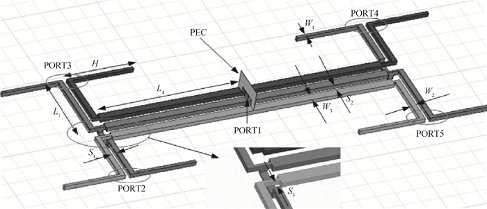
Fig. 1.
(a) Section plane of the dipole. (b) Plan form of the dipole.
SEMICONDUCTOR INTEGRATED CIRCUITS
Jun Luo, Yan Wang and Ruifeng Yue
Corresponding author: Luo Jun, luojun51211314@gmail.com
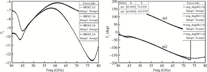
Abstract: This design is presented of a 2X2 planar array, with a half-wave dipole antenna to be its element, on a new substrate material, Schott Borofloat, with CMOS technology in the 60 GHz band. In the proposed structure, all the designs are based on the CMOS technology and similar performance could be achieved with the same size in contrast to the design on low-temperature co-fired ceramic (LTCC). This could lead to the improving of the compatibility with the CMOS IC process, the design cost and the design precision which is restricted in the LTCC process. The simulated -10 dB bandwidth of the array is from 58 to 64 GHz. A peak gain of 9.4 dBi is achieved. Good agreement on return loss is achieved between simulations and measurements.
Keywords: Schott Borofloat, array, half-wave dipole, 60 GHz, CMOS technology
| [1] |
Zhang Y P, Liu D X. Antenna-on-chip and antenna-in-package solutions to highly integrated millimeter-wave devices for wireless communications. IEEE Trans Antennas Propagation, 2009, 57(10):2830 doi: 10.1109/TAP.2009.2029295
|
| [2] |
Mendes P M, Sinaga S, Polyakov A, et al. Wafer-level integration of on-chip antennas and RF passives using high-resistivity polysilicon substrate technology. Proc Electronic Components Technology Conf, 2004 http://ieeexplore.ieee.org/document/1320376/authors
|
| [3] |
Kim J G, Lee H S, Lee H S, et al. 60-GHz CPW-fed post-supported patch antenna using micromachining technology. IEEE Microw Wireless Compon Lett, 2005, 15(10):635 doi: 10.1109/LMWC.2005.856690
|
| [4] |
Lamminen A E I, Saily J, Vimpari A R. 60-GHz patch antennas and arrays on LTCC with embedded-cavity substrates. IEEE Trans Antennas Propagation, 2008, 56(9):2865 doi: 10.1109/TAP.2008.927560
|
| [5] |
Zhang Y P, Sun M, Chua K M, et al. Integration of slot antenna in LTCC package for 60 GHz radios. Electron Lett, 2008, 44(5):330 doi: 10.1049/el:20083352
|
| [6] |
Sun M, Guo Y X, Karim M F, et al. Integrated 60-GHz LTCC circularly polarized antenna array. IEEE International Symposium on Radio-Frequency Integration Technology, 2009 http://ieeexplore.ieee.org/document/5383656/keywords
|
| [7] |
Chen X P, Wu K, Han L, et al. Low-cost high gain planar antenna array for 60-GHz band applications. IEEE Trans Antennas Propagation, 2010, 58(6):2126 doi: 10.1109/TAP.2010.2046861
|
| [8] |
Sun M, Zhang Y P, Chua K M, et al. Integration of Yagi antenna in LTCC package for differential 60-GHz radio. IEEE Trans Antennas Propagation, 2008, 56(8):2780 doi: 10.1109/TAP.2008.927577
|
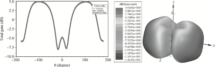
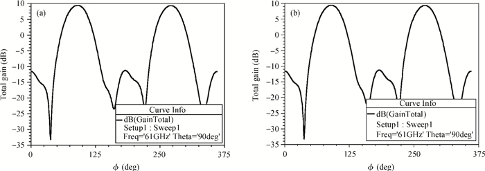
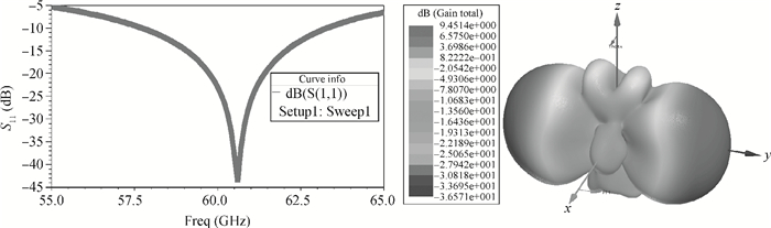

Table 1. Electrical properties.

|
Table 2. Structure size.

|
Table 3. Comparison with designs in references.

|
| [1] |
Zhang Y P, Liu D X. Antenna-on-chip and antenna-in-package solutions to highly integrated millimeter-wave devices for wireless communications. IEEE Trans Antennas Propagation, 2009, 57(10):2830 doi: 10.1109/TAP.2009.2029295
|
| [2] |
Mendes P M, Sinaga S, Polyakov A, et al. Wafer-level integration of on-chip antennas and RF passives using high-resistivity polysilicon substrate technology. Proc Electronic Components Technology Conf, 2004 http://ieeexplore.ieee.org/document/1320376/authors
|
| [3] |
Kim J G, Lee H S, Lee H S, et al. 60-GHz CPW-fed post-supported patch antenna using micromachining technology. IEEE Microw Wireless Compon Lett, 2005, 15(10):635 doi: 10.1109/LMWC.2005.856690
|
| [4] |
Lamminen A E I, Saily J, Vimpari A R. 60-GHz patch antennas and arrays on LTCC with embedded-cavity substrates. IEEE Trans Antennas Propagation, 2008, 56(9):2865 doi: 10.1109/TAP.2008.927560
|
| [5] |
Zhang Y P, Sun M, Chua K M, et al. Integration of slot antenna in LTCC package for 60 GHz radios. Electron Lett, 2008, 44(5):330 doi: 10.1049/el:20083352
|
| [6] |
Sun M, Guo Y X, Karim M F, et al. Integrated 60-GHz LTCC circularly polarized antenna array. IEEE International Symposium on Radio-Frequency Integration Technology, 2009 http://ieeexplore.ieee.org/document/5383656/keywords
|
| [7] |
Chen X P, Wu K, Han L, et al. Low-cost high gain planar antenna array for 60-GHz band applications. IEEE Trans Antennas Propagation, 2010, 58(6):2126 doi: 10.1109/TAP.2010.2046861
|
| [8] |
Sun M, Zhang Y P, Chua K M, et al. Integration of Yagi antenna in LTCC package for differential 60-GHz radio. IEEE Trans Antennas Propagation, 2008, 56(8):2780 doi: 10.1109/TAP.2008.927577
|


Article views: 2849 Times PDF downloads: 13 Times Cited by: 0 Times
Received: 26 April 2013 Revised: 26 June 2013 Online: Published: 01 November 2013
| Citation: |
Jun Luo, Yan Wang, Ruifeng Yue. 60-GHz array antenna with standard CMOS technology on Schott Borofloat[J]. Journal of Semiconductors, 2013, 34(11): 115006. doi: 10.1088/1674-4926/34/11/115006
****
J Luo, Y Wang, R F Yue. 60-GHz array antenna with standard CMOS technology on Schott Borofloat[J]. J. Semicond., 2013, 34(11): 115006. doi: 10.1088/1674-4926/34/11/115006.

|
| [1] |
Zhang Y P, Liu D X. Antenna-on-chip and antenna-in-package solutions to highly integrated millimeter-wave devices for wireless communications. IEEE Trans Antennas Propagation, 2009, 57(10):2830 doi: 10.1109/TAP.2009.2029295
|
| [2] |
Mendes P M, Sinaga S, Polyakov A, et al. Wafer-level integration of on-chip antennas and RF passives using high-resistivity polysilicon substrate technology. Proc Electronic Components Technology Conf, 2004 http://ieeexplore.ieee.org/document/1320376/authors
|
| [3] |
Kim J G, Lee H S, Lee H S, et al. 60-GHz CPW-fed post-supported patch antenna using micromachining technology. IEEE Microw Wireless Compon Lett, 2005, 15(10):635 doi: 10.1109/LMWC.2005.856690
|
| [4] |
Lamminen A E I, Saily J, Vimpari A R. 60-GHz patch antennas and arrays on LTCC with embedded-cavity substrates. IEEE Trans Antennas Propagation, 2008, 56(9):2865 doi: 10.1109/TAP.2008.927560
|
| [5] |
Zhang Y P, Sun M, Chua K M, et al. Integration of slot antenna in LTCC package for 60 GHz radios. Electron Lett, 2008, 44(5):330 doi: 10.1049/el:20083352
|
| [6] |
Sun M, Guo Y X, Karim M F, et al. Integrated 60-GHz LTCC circularly polarized antenna array. IEEE International Symposium on Radio-Frequency Integration Technology, 2009 http://ieeexplore.ieee.org/document/5383656/keywords
|
| [7] |
Chen X P, Wu K, Han L, et al. Low-cost high gain planar antenna array for 60-GHz band applications. IEEE Trans Antennas Propagation, 2010, 58(6):2126 doi: 10.1109/TAP.2010.2046861
|
| [8] |
Sun M, Zhang Y P, Chua K M, et al. Integration of Yagi antenna in LTCC package for differential 60-GHz radio. IEEE Trans Antennas Propagation, 2008, 56(8):2780 doi: 10.1109/TAP.2008.927577
|

 WeChat ID
Journal of Semiconductors © 2017 All Rights Reserved 京ICP备05085259号-2

 DownLoad: