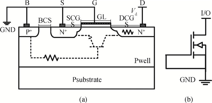
Fig. 1.
(a) Cross-section of GGNMOS and (b) its configuration.
SEMICONDUCTOR DEVICES
Daoxun Wu, Lingli Jiang, Hang Fan, Jian Fang and Bo Zhang
Corresponding author: Wu Daoxun, wudx_2008@126.com
Abstract: Contrary to general understanding, a test result shows that devices with a shorter channel length have a degraded ESD performance in the advanced silicided CMOS process. Such a phenomenon in a gate-grounded NMOSFET (GGNMOS) was investigated, and the current spreading effect was verified as the predominant factor. Due to transmission line pulse (TLP) measurements and Sentaurus technology computer aided design (TCAD) 2-D numerical simulations, parameters such as current gain, on-resistance and power density were discussed in detail.
Keywords: ESD, channel length, GGNMOS, current spreading
| [1] |
Salman A, Gauthier R, Stadler W, et al. NMOSFET ESD self-protection strategy and underlying failure mechanism in advanced 0.13-μm CMOS technology. IEEE Trans Device Mater Reliab, 2002, 12(1):2
|
| [2] |
Oh K H, Banerjeel K, Duvwg C, et al. Non-uniform conduction induced reverse channel length dependence of ESD reliability for silicided NMOS transistors. IEEE IEDM, 2002:341 http://ieeexplore.ieee.org/document/1175848/?arnumber=1175848
|
| [3] |
Pogany D, Johnsson D, Bychikhin S, et al. Measuring holding voltage related to homogeneous current flow in wide ESD protection structures using multilevel TLP. IEEE Trans Electron Devices, 2011, 58(2):411 doi: 10.1109/TED.2010.2093143
|
| [4] |
Dong S, Du X, Han Y, et al. Analysis of 65 nm technology grounded-gate NMOS for on-chip ESD protection applications. IEEE Electron Lett, 2008, 44(19):1129 doi: 10.1049/el:20081073
|
| [5] |
Lee J H, Wu K M, Huang S C, et al. The dynamic current distribution of a multi-fingered GGNMOS under high current stress and HBMESD events. IEEE Reliab Phys Symp Proc, 2006:629 http://ieeexplore.ieee.org/document/4017237/
|
| [6] |
Chen T Y, Ker M D. Analysis on the dependence of layout parameters on ESD robustness of CMOS devices for manufacturing in deep-submicron CMOS process. IEEE Trans Semicond Manufacturing, 2003, 16(3):486 doi: 10.1109/TSM.2003.815200
|
| [7] |
Bock K, Russ C, Badenes G, et al. Influence of well profile and gate length on the ESD performance of a fully silicided 0.25μm CMOS technology. IEEE Trans Components, Packaging, and Manufactory Technology-Part C, 1998, 21(4):286 doi: 10.1109/3476.739178
|
| [8] |
Bock K, Keppens B, De Heyn V, et al. Influence of gate length on ESD-performance for deep submicron CMOS technology. EOS/ESD Symposium, 1999:95 http://dblp.uni-trier.de/db/journals/mr/mr41.html
|
| [9] |
Sze S M. Physics of semiconductor devices. 3rd ed. New York: Wiley, 2007: 257
|
| [10] |
Chen X B, Zhang Q Z. Theory and design of transistors. 2nd ed. Beijing: Publishing House of Electronics Industry, 2008: 132(in Chinese)
|
| [11] |
Li M Z, Wei G P, Chen X B. Analysis of local electro-thermal effects of LDM OS power device. Chinese Journal of Semiconductors, 2005, 26(9):1823 http://econpapers.repec.org/article/eeerensus/v_3a58_3ay_3a2016_3ai_3ac_3ap_3a1500-1520.htm
|
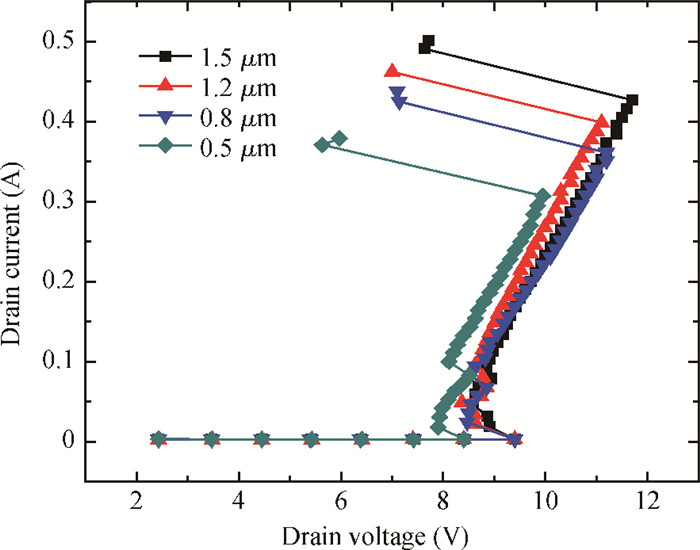
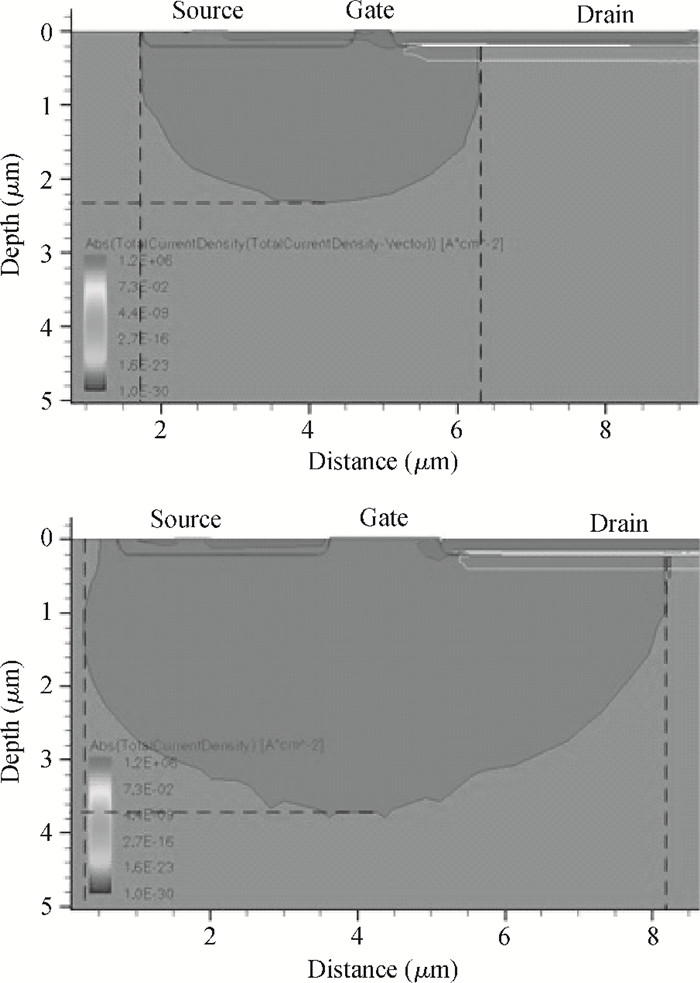
Table 1. Ratio values of Vt1/Vh.

|
| [1] |
Salman A, Gauthier R, Stadler W, et al. NMOSFET ESD self-protection strategy and underlying failure mechanism in advanced 0.13-μm CMOS technology. IEEE Trans Device Mater Reliab, 2002, 12(1):2
|
| [2] |
Oh K H, Banerjeel K, Duvwg C, et al. Non-uniform conduction induced reverse channel length dependence of ESD reliability for silicided NMOS transistors. IEEE IEDM, 2002:341 http://ieeexplore.ieee.org/document/1175848/?arnumber=1175848
|
| [3] |
Pogany D, Johnsson D, Bychikhin S, et al. Measuring holding voltage related to homogeneous current flow in wide ESD protection structures using multilevel TLP. IEEE Trans Electron Devices, 2011, 58(2):411 doi: 10.1109/TED.2010.2093143
|
| [4] |
Dong S, Du X, Han Y, et al. Analysis of 65 nm technology grounded-gate NMOS for on-chip ESD protection applications. IEEE Electron Lett, 2008, 44(19):1129 doi: 10.1049/el:20081073
|
| [5] |
Lee J H, Wu K M, Huang S C, et al. The dynamic current distribution of a multi-fingered GGNMOS under high current stress and HBMESD events. IEEE Reliab Phys Symp Proc, 2006:629 http://ieeexplore.ieee.org/document/4017237/
|
| [6] |
Chen T Y, Ker M D. Analysis on the dependence of layout parameters on ESD robustness of CMOS devices for manufacturing in deep-submicron CMOS process. IEEE Trans Semicond Manufacturing, 2003, 16(3):486 doi: 10.1109/TSM.2003.815200
|
| [7] |
Bock K, Russ C, Badenes G, et al. Influence of well profile and gate length on the ESD performance of a fully silicided 0.25μm CMOS technology. IEEE Trans Components, Packaging, and Manufactory Technology-Part C, 1998, 21(4):286 doi: 10.1109/3476.739178
|
| [8] |
Bock K, Keppens B, De Heyn V, et al. Influence of gate length on ESD-performance for deep submicron CMOS technology. EOS/ESD Symposium, 1999:95 http://dblp.uni-trier.de/db/journals/mr/mr41.html
|
| [9] |
Sze S M. Physics of semiconductor devices. 3rd ed. New York: Wiley, 2007: 257
|
| [10] |
Chen X B, Zhang Q Z. Theory and design of transistors. 2nd ed. Beijing: Publishing House of Electronics Industry, 2008: 132(in Chinese)
|
| [11] |
Li M Z, Wei G P, Chen X B. Analysis of local electro-thermal effects of LDM OS power device. Chinese Journal of Semiconductors, 2005, 26(9):1823 http://econpapers.repec.org/article/eeerensus/v_3a58_3ay_3a2016_3ai_3ac_3ap_3a1500-1520.htm
|


Article views: 4588 Times PDF downloads: 110 Times Cited by: 0 Times
Received: 09 June 2012 Revised: 24 September 2012 Online: Published: 01 February 2013
| Citation: |
Daoxun Wu, Lingli Jiang, Hang Fan, Jian Fang, Bo Zhang. Analysis on the positive dependence of channel length on ESD failure current of a GGNMOS in a 5 V CMOS[J]. Journal of Semiconductors, 2013, 34(2): 024004. doi: 10.1088/1674-4926/34/2/024004
****
D X Wu, L L Jiang, H Fan, J Fang, B Zhang. Analysis on the positive dependence of channel length on ESD failure current of a GGNMOS in a 5 V CMOS[J]. J. Semicond., 2013, 34(2): 024004. doi: 10.1088/1674-4926/34/2/024004.

|
| [1] |
Salman A, Gauthier R, Stadler W, et al. NMOSFET ESD self-protection strategy and underlying failure mechanism in advanced 0.13-μm CMOS technology. IEEE Trans Device Mater Reliab, 2002, 12(1):2
|
| [2] |
Oh K H, Banerjeel K, Duvwg C, et al. Non-uniform conduction induced reverse channel length dependence of ESD reliability for silicided NMOS transistors. IEEE IEDM, 2002:341 http://ieeexplore.ieee.org/document/1175848/?arnumber=1175848
|
| [3] |
Pogany D, Johnsson D, Bychikhin S, et al. Measuring holding voltage related to homogeneous current flow in wide ESD protection structures using multilevel TLP. IEEE Trans Electron Devices, 2011, 58(2):411 doi: 10.1109/TED.2010.2093143
|
| [4] |
Dong S, Du X, Han Y, et al. Analysis of 65 nm technology grounded-gate NMOS for on-chip ESD protection applications. IEEE Electron Lett, 2008, 44(19):1129 doi: 10.1049/el:20081073
|
| [5] |
Lee J H, Wu K M, Huang S C, et al. The dynamic current distribution of a multi-fingered GGNMOS under high current stress and HBMESD events. IEEE Reliab Phys Symp Proc, 2006:629 http://ieeexplore.ieee.org/document/4017237/
|
| [6] |
Chen T Y, Ker M D. Analysis on the dependence of layout parameters on ESD robustness of CMOS devices for manufacturing in deep-submicron CMOS process. IEEE Trans Semicond Manufacturing, 2003, 16(3):486 doi: 10.1109/TSM.2003.815200
|
| [7] |
Bock K, Russ C, Badenes G, et al. Influence of well profile and gate length on the ESD performance of a fully silicided 0.25μm CMOS technology. IEEE Trans Components, Packaging, and Manufactory Technology-Part C, 1998, 21(4):286 doi: 10.1109/3476.739178
|
| [8] |
Bock K, Keppens B, De Heyn V, et al. Influence of gate length on ESD-performance for deep submicron CMOS technology. EOS/ESD Symposium, 1999:95 http://dblp.uni-trier.de/db/journals/mr/mr41.html
|
| [9] |
Sze S M. Physics of semiconductor devices. 3rd ed. New York: Wiley, 2007: 257
|
| [10] |
Chen X B, Zhang Q Z. Theory and design of transistors. 2nd ed. Beijing: Publishing House of Electronics Industry, 2008: 132(in Chinese)
|
| [11] |
Li M Z, Wei G P, Chen X B. Analysis of local electro-thermal effects of LDM OS power device. Chinese Journal of Semiconductors, 2005, 26(9):1823 http://econpapers.repec.org/article/eeerensus/v_3a58_3ay_3a2016_3ai_3ac_3ap_3a1500-1520.htm
|

 WeChat ID
Journal of Semiconductors © 2017 All Rights Reserved 京ICP备05085259号-2

 DownLoad: