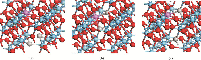
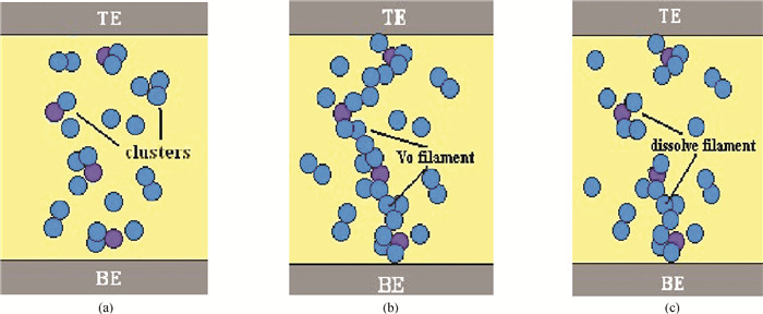
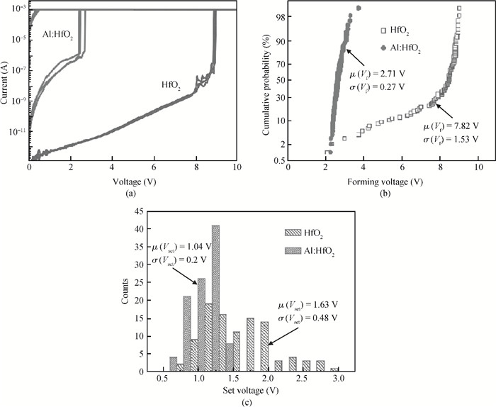
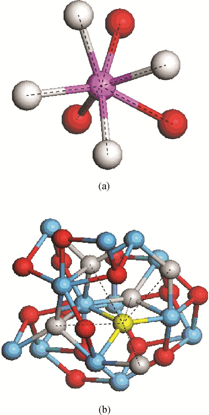
1. School of Electronic and Information Engineering, Anhui University, Hefei 230601, ChinaSchool of Electronic and Information Engineering, Anhui University, Hefei 230601, China
2. Laboratory of Nano-Fabrication and Novel Device Integrated Technology, Institute of Microelectronics, Chinese Academy of Sciences, Beijing 100029, ChinaLaboratory of Nano-Fabrication and Novel Device Integrated Technology, Institute of Microelectronics, Chinese Academy of Sciences, Beijing 100029, China
3. Internet Network Information Center, Institutes of Physical Science, Chinese Academy of Sciences, Hefei 230031, ChinaInternet Network Information Center, Institutes of Physical Science, Chinese Academy of Sciences, Hefei 230031, China
Abstract: The physical mechanism of doping effects on switching uniformity and operation voltage in Al-doped HfO2 resistive random access memory (RRAM) devices is proposed from another perspective:defects interactions, based on first principle calculations. In doped HfO2, dopant is proved to have a localized effect on the formation of defects and the interactions between them. In addition, both effects cause oxygen vacancies (VO) to have a tendency to form clusters and these clusters are easy to form around the dopant. It is proved that this process can improve the performance of material through projected density of states (PDOS) analysis. For VO filament-type RRAM devices, these clusters are concluded to be helpful for the controllability of the switching process in which oxygen vacancy filaments form and break. Therefore, improved uniformity and operation voltage of Al-doped HfO2 RRAM devices is achieved.
Recently the conduction mechanism of resistive random access memory (RRAM) has been drawing extensive research. Many researchers have used the conductive filament model to explain the resistive switch behavior of the RRAM. For most conduction filament-type RRAM devices, rupture and the formation of localized conduction filaments (CFs) is the main physical mechanism of resistive switching behaviors. The CFs, which may consist of either an intrinsic oxygen vacancy (VO) from crystal or metal ions resolving from an electrode[1-3], plays a crucial role in the resistive switching behavior of the RRAM. However, the RRAM devices often show a large variation in switching voltage due to the random growth/rupture of the CFs[4]. This random characteristic often makes it difficult for the CFs to form or break along the same path in each switching cycle. Therefore, in order to improve the uniformity of operation voltage, a controllable mechanism of CF growth should be established. Several works have been done to address this problem. Some research has improved the controllability of CFs by a thin GST interface layer[5], metallic nanocrystal (NC)[6], lighting rod effect[7] and doping effects[8, 9]. From previous studies, VO properties in the functional layer material of RRAM devices such as HfO2[10] or Al doped HfO2[11, 18, 20] have been addressed. The formation energy of VO (EfVO) is significantly influenced by doping trivalent ions[8, 9]. Up to now, however, some researchers have mainly focused on the relationship between EfVO and dopants characters, such as chemical valence and dopant ionic radius[12, 13] in doped materials. They neglected the relationship between EfVO and the distance between VO and dopants. Moreover, after VO being formed near the dopant, there will be an interaction between the dopant and charge-compensating vacancy to form a distinct defect cluster[12, 14]. Fewer researchers have found a relationship between the interaction of defects and electrical properties of RRAM devices. Interactions between oxygen vacancies also exist, as found in NiO[15]. In a Ni/NiO RRAM device, the formation and rupture of an oxygen vacancy chain is due to the presence of VO interactions which affect the RS characters[16]. In this paper, we adopt the first principle method to confirm doping localized effects and discuss the relationship between defect interactions and electrical properties of an Al-doped HfO2 RRAM device. From another aspect we could understand the relationship of material properties and device electrical characteristics and it provides guidance for the optimization design of RRAM device material. We focus on the structural and energetic aspects in this paper. A detailed discussion on the electronic structures will be given in a separate paper.
2.
Material and methods
In this study, the first-principle calculations are based on the density-functional theory (DFT) within the Perdew Burke Ernzerhof (GGA-PBE) for the exchange-correlation potential, and Vanderbilt type ultrasoft pseudopotentials for core-valance interaction, as implemented in the CASTEP code[17]. The valence configurations of the pseudopotentials are 5p65d26s2 for Hf, 2s22p4 for O. The plane wave set basis cutoff energy is 340 eV, k-points sampling is performed at 2 × 2 × 2 special points in a Monkhorst-Pack grid. Geometries of supercells are fully relaxed until atomic forces are smaller than 0.03 eV/Å. A jellium background is used to neutralize the lattice in the calculations for charged defects. To calculate the relative parameters, a supercell (2 × 2 × 2) of monoclinic HfO2 containing 96 atoms is constructed. The Coulomb interaction between charged defects in different periodic cells is calculated using the Makov-Payne scheme, and due to the large size of the supercell separating the periodic defect images by over 10 Å, the corresponding image charge correction is below 0.1 eV. Oxygen atoms are removed from the supercell in order to model the vacancy defects, one doping Al atom replaces the Hf site in this supercell to build a doping system, which is energetically favorable under oxygen-rich conditions[18]. Corresponding to the above, it is equivalent to implanting Al atoms forming about 1% concentration into the HfO2 layer.
3.
Results and discussions
The formation energy of charged VO is defined as[19]
Ef(XQ)=Etot(XQ)−Etot(bulk)+Q(εf+εv+ΔV)+μO,
(1)
where Etot(XQ) and Etot(bulk) are the total energy of the supercell containing XQ with charge Q and the supercell without the XQ, respectively. εf is the Fermi level, referenced to the edge of valence band (VB) εv, ΔV is the shift of εv due to the introduced charge of XQ defects in the supercell. μO is the chemical potential of oxygen, and it is half of the oxygen molecule energy in this calculation. Due to the low concentration of Al, V+1O is chosen to be calculated for study doping effects[20]. The εf is set as 0 eV when the formation energy of V+1O is calculated.
As we know, there are two types of oxygen vacancies in monoclinic hafnia: threefold and fourfold-coordinated (VO3 and VO4, respectively)[10]. As shown in Fig. 1, due to the asymmetry of the monoclinic HfO2, there may be different distances between one dopant and two types of oxygen vacancies in the same position of NN (nearest neighbor), NNN (next-nearest neighbor) or even as far as NNNN (next-next-nearest neighbor) positions.
Figure
1.
(Color online) (a) Seven oxygen vacancies include VO3 and VO4 (the red and white balls, respectively) at the NN position to Al atom (the purple ball). (b) Oxygen vacancies (the gray balls) with different distances at the NN positions of one VO3 (the yellow ball).
As shown by the computed results in Fig. 2, trivalent Al has significantly reduced both EfVO of V+1O3 and V+1O4, compared with the un-doped HfO2. This is due to the formation of Hf-O-Al[20]. It is noticed in Fig. 2(a) that the formation energy of V+1O3 and that of V+1O4 at the NN position to the Al are both smaller than that at other positions. With the distance increasing, the doping effect on the EfVO will be weakened, which indicates that the dopant will enhance the formation of VO which at nearly positions. Compared with the doping effect, the formation energy of V+1O3 and V+1O4 which are at different distances from the other neutral VO3 in pure HfO2 are also calculated, as shown in Fig. 2(b). It is found that as the distance increases, the deviation of EfVO with respect to distance does not exceed 1%. This indicates one VO has no obvious influence on the formation of the other VO.
Figure
2.Efvo of V+1O3, V+1O4. (a) At different positions to Al atom. (b) At different positions to one VO3. The εf is set as 0 eV.
In this paper, the achieved stability of CFs is due to the localization effect of dopant. The stability of VO not only depends on its formation energy, but relates to the interaction between the dopant and VO. The interaction with VO should also be taken into account. These interactions should not be neglected when we investigate the RS behaviors of RRAM devices. The interaction energy (Eint) is calculated when two defects are in different distances away, the general relationship is the following:
Eint=Ecluster−∑componentEisolate−defect.
(2)
The computation results are shown in Fig. 3. It is known that two defects with opposite charge: Al−1Hf and V+1O/V+2O, form the (AlHf-VO)0 and (AlHf-VO)+1, respectively[18]. In this paper, we choose the neutral complex (AlHf -VO)0 to study the interaction energy between the dopant and VO. Here we show Eint between Al−1Hf and V+1O, the vertical axis denotes Eint. The lower Eint is, the more the configuration of Al−1Hf and V+1O is stable. The horizontal axis represents the relative position of Al−1Hf and V+1O. It is shown in Fig. 3(a) that VO is stable at the first nearest O sites of Al−1Hf. With increasing distance, the dopant's localized effect will be weakened, as the case of Efvo. It may be concluded that VO is effectively trapped at these sites due to an attractive coulombic interaction between Al−1Hf and V+1O, or local structural modifications[21] induced by dopants of different sizes compared to the host Hf+4 ions would be another possible reason to account for the defect interaction energy. Recently it has been shown that V+1O and V0O will stabilize a cohesive filament in TiO2-based RRAM devices[22]. Then the Eint between two oxygen vacancies with different charge states in HfO2 was calculated. In Figs. 3(b) and 3(c), some interaction energies between oxygen vacancies are negative although repulsive interactions are expected between defects with the same charge states. With increasing distance, the Eint of the VO3-VO3 pair has obviously changed while Eint of VO3-VO4 has a small deviation. The obvious differences of the two types of VO pairs may be due to different influences from structural modifications or electron interactions. The maximum interaction energy is achieved when two VO's are singly ionized. These may be due to atomic rearrangements and hybridization between vacancy orbitals[23]. A similar effect has been observed in NiO[15-16] as well.
Figure
3.Eint of six different configurations of defects: Eint between defects related to distance. (a) Between Al and VO3/VO4. (b), (c) Between two VO in pure HfO2, the VO are neutral and singly ionized.
To further investigate the influence of defect clusters on the characteristics of doped HfO2, the PDOS of each different configurations has been calculated, as shown in Fig. 4. From the PDOS analysis, the gap between defect level and conduction-band minimum (CBM) in Fig. 4(a) is smaller than that in Fig. 4(b), respectively, indicating that when VO is trapped by the dopant at the adjacent position, the defect level will move upward. Based on the physical model of bipolar resistive switching behavior established by Gao[24], it will cause the reduction of the critical electrical field to reset the devices and result in faster reset speed of RRAM devices[9]. Since Figure 5 has shown the PDOS of VO-VO pairs in pure HfO2, the gap between the defect level and the conduction band minimum has no obvious change, however, when VO at the NN site of the other VO, the peak position of the O(p) orbital has a deviation of 0.092 eV from the peak position of Hf(d) orbital due to the electronic interaction between these orbitals. When the oxygen vacancies form a cluster, the defect states overlap and energy levels are split due to bonding or antibonding combinations of wave functions[15]. From band structure analysis which is not shown in this paper, two oxygen vacancies create two defect energy levels within the band gap region, as the same results that oxygen vacancy clusters may introduce a subband in the gap[25].
Figure
4.
PDOS of Al doped HfO2 with VO3. (a) At the NN. (b) At the NNN position to the dopant. The green line is the p state which mainly consists of the Hf(p) state and the O(p) state, the blue line is the d state which consists of the Hf(d) state.
Figure
5.
PDOS of HfO2 with one VO3. (a) At the NN. (b) At the NNN position to the other VO3. The green line is the p state which mainly consists of the Hf(p) state and the O(p) state, the blue line is the d state which consists of the Hf(d) state.
Figure 6 shows the different location of the two oxygen vacancies with respect to the Al cation. It is clear that the configuration corresponding to Fig. 6(a) has the lowest energy (-39936.97 eV) due to defect interactions, indicating that the oxygen vacancy clusters will be stable near the dopants. Comparing Fig. 6(b) (-39937.28 eV) and Fig. 6(c) (-39937.16 eV), it also confirms that the oxygen vacancies tend to form clusters in doped HfO2 which is used as the function layer of RRAM devices.
Figure
6.
Schematic view of VO in doped HfO2 with different configurations. (a) VO pair far away from the Al. (b) VO pair at NN position from Al. (c) One VO at the NN sites while the other one at another site far from Al. The pink and gray balls denote Al impurity and VO, respectively.
As discussed above, it can be concluded that there is a relationship between the defect interaction and the process of "forming" and "set/reset" in the Al-doped RRAM device, which has been illustrated in Fig. 7. This interaction has two effects on the device resistive switch behaviors. First, during the working state, voltage is applied to the whole dielectrics and it enhances the generation of oxygen vacancies. From analysis above, oxygen vacancies will spontaneously generate and form clusters close to the dopants due to the interaction of VO-VO and Al-VO pairs, as shown in Fig. 7(a). With the help of clusters, consequently, the CFs will be steadily formed around the Al-doping sites by linking these clusters, as shown in Fig. 7(b). The distribution of the forming voltage (Vforming) and set voltage (Vset) of the RRAM device will be improved due to this stable process, which is confirmed by experimental results as shown in Figs. 8(b) and 8(c). Then a better uniformity of Vforming and Vset has been achieved[8] Second, during "forming" and each"set/reset"cycle, fewer VO are needed to link the dissolved Vo clusters, as shown in Fig. 7(c). This will mean that the strength of the electric field that can generate VO becomes lower. This inference is also confirmed by experimental results as shown in Figs. 8(a) and 8(c) in which the Vforming and Vset are both reduced[8].
Figure
7.
Schematic views to illustrate the formation of CF in the switching process. (a) Before the "forming" process. (b) After the "forming" process. (c) After the "reset" process. The purple balls and blue balls denote Al impurity and oxygen vacancies, respectively.
Figure
8.
(a) I-V curves of the forming process. A lower forming voltage is measured in Al-doped HfO2 devices. (b) Uniformity of the forming voltage is significantly improved by Al doping HfO2. (c) Reduction and better uniformity of set voltage is achieved in Al-doped HfO2 devices[8].
Based on the first principle methods, it is proved that the doping effects can improve the uniformity of oxide-based RRAM device from the perspective of defect interactions. The dopants have localization effects on not only formation energy but interactions of oxygen vacancies in the neighbourhood. These intrinsic defects tend to form clusters due to interactions between VO-VO and dopant-VO pairs. For localized CFs, these clusters will be helpful for improving the stability of the growth/rupture process. Therefore, they will optimize the resistive switching process of RRAM. This paper provides another perspective to understand the physical mechanism of doping effects on oxide-based RRAM devices.
References
[1]
Yang Y, Pan F, Liu Q, et al. Fully room-temperature-fabricated nonvolatile resistive memory for ultrafast and high-density memory application. Nano Lett, 2009, 9(4):1636 doi: 10.1021/nl900006g
[2]
Waser R, Aono M. Nanoionics based resistive switching memories. Nature Mater, 2007, 6(11):833 doi: 10.1038/nmat2023
[3]
Zhou M X, Zhao Q, Zhang W, et al. The conductive path in HfO2:first principle study. Journal of Semiconductors, 2012, 33(7):072002 doi: 10.1088/1674-4926/33/7/072002
[4]
Li Y T, Wang Y, Liu S, et al. Improvement of resistive switching uniformity in TiOx films by nitrogen annealing. J Korean Phys Soc, 2011, 58(3):L407
[5]
Lv H, Wan H, Tang T. Improvement of resistive switching uniformity by introducing a thin GST interface layer. IEEE Electron Device Lett, 2010, 31(9):978 doi: 10.1109/LED.2010.2055534
[6]
Liu Q, Long S, Lv H, et al. Controllable growth of nanoscale conductive filaments in solid electrolyte based ReRAM by using a metal nanocrystal covered bottom electrode. ACSnano, 2010, 4(10):6162
[7]
Park J, Jo M, Lee J, et al. Improved switching uniformity and speed in filament type RRAM using lighting rod effect. IEEE Electron Device Lett, 2011, 32(1):63 doi: 10.1109/LED.2010.2084560
[8]
Gao B, Zhang H, Yu S, et al. Oxide based RRAM:uniformity improvement using a new material oriented methodology. Symp on VLSI Technol, 2009:30 http://ieeexplore.ieee.org/document/5200623/
[9]
Zhang H W, Liu L F, Gao B, et al. Gd doping effect on performance of HfO2 based resistive switching memory devices using implantation approach. Appl Phys Lett, 2011, 98:042105 doi: 10.1063/1.3543837
[10]
Foster A S, Lopez Gejo F, Shluger A L, et al. Vacancy and interstitial defects in hafnia. Phys Rev B, 2002, 65:174117 doi: 10.1103/PhysRevB.65.174117
[11]
Hou Z F, Gong X G, Li Q. Al-induced reduction of the oxygen diffusion in HfO2:an ab initio study. J Phys:Condense Matter, 2008, 20:135206 doi: 10.1088/0953-8984/20/13/135206
[12]
Umezawa N, Sato M, Shiraishi M. Reduction in charged defects associated with oxygen vacancies in hafnia by magnesium incorporation:first-principles study. Appl Phys Lett, 2008, 93:223104 doi: 10.1063/1.3040306
[13]
Zhang H, Gao B, Sun B, et al. Ionic doping effect in ZrO2 resistive switching memory. Appl Phys Lett, 2010, 96:123502 doi: 10.1063/1.3364130
[14]
Nadimi E, Ottking R, Plänitz P, et al. Interaction of oxygen vacancies and lanthanum in Hf-based high-k dielectrics:an ab initio investigation. J Phys Condens Matter, 2011, 23:365502 doi: 10.1088/0953-8984/23/36/365502
[15]
Park S, Ahn H S, Lee C K, et al. Interaction and ordering of vacancy defects in NiO. Phys Rev B, 2008, 77:134103 doi: 10.1103/PhysRevB.77.134103
[16]
He L, Liao Z, Wu H, et al. Memory and threshold resistance switching in Ni/NiO core-shell nanowires. Nanoletters, 2011, 11(11):4601 doi: 10.1021/nl202017k
[17]
Segall M D, Lindan P J D, Probert M J, et al. First principles simulation:ideas, illustrations and the CASTEP code. J Phys Condens Matter, 2002, 14:2717 doi: 10.1088/0953-8984/14/11/301
[18]
Li Quan, Koo K M, Lau W M, et al. Effects of Al addition on the native defects in hafnia. Appl Phys Lett, 2006, 88:182903 doi: 10.1063/1.2196470
[19]
Van de Walle C G, Neugebauer J. First principles calculations for defects and impurities:applications to Ⅲ-nitrides. J Appl Phys, 2004, 95:3851 doi: 10.1063/1.1682673
[20]
Peng C, Chang W, Lee Y, et al. Electrochem improvement of resistive switching stability of HfO2 films with Al doping by atomic layer deposition. Solid-State Lett, 2012, 15(4):H88 http://esl.ecsdl.org/content/15/4/H88.full.pdf
[21]
Nakayama M, Martin M. First-principles study on defect chemistry and migration of oxide ions in ceria doped with rare-earth cations. Phys Chem Chem Phys, 2009, 11:3241 doi: 10.1039/b900162j
[22]
Kamiya K, Yang M Y, Park S G, et al. On-off switching mechanism of resistive random access memories based on the formation and disruption of oxygen vacancy conduction channels. Appl Phys Lett, 2012, 100:073502 doi: 10.1063/1.3685222
[23]
Finocchi F, Goniakowski J, Noguera C. Interaction between oxygen vacancies on MgO. Phys Rev B, 1999, 59(7):5179
[24]
Gao B, Sun B, Zhang H, et al. Unified physical model of bipolar oxide based resistive switching memory. IEEE Electron Device Lett, 2009, 30:1326 doi: 10.1109/LED.2009.2032308
[25]
Wu X, Migas D B, Li X, et al. Role of oxygen vacancies in HfO2-based gate stack breakdown. Appl Phys Lett, 2010, 96:172901 doi: 10.1063/1.3416912
Fig. 1.
(Color online) (a) Seven oxygen vacancies include VO3 and VO4 (the red and white balls, respectively) at the NN position to Al atom (the purple ball). (b) Oxygen vacancies (the gray balls) with different distances at the NN positions of one VO3 (the yellow ball).
Fig. 3.Eint of six different configurations of defects: Eint between defects related to distance. (a) Between Al and VO3/VO4. (b), (c) Between two VO in pure HfO2, the VO are neutral and singly ionized.
Fig. 4.
PDOS of Al doped HfO2 with VO3. (a) At the NN. (b) At the NNN position to the dopant. The green line is the p state which mainly consists of the Hf(p) state and the O(p) state, the blue line is the d state which consists of the Hf(d) state.
Fig. 5.
PDOS of HfO2 with one VO3. (a) At the NN. (b) At the NNN position to the other VO3. The green line is the p state which mainly consists of the Hf(p) state and the O(p) state, the blue line is the d state which consists of the Hf(d) state.
Fig. 6.
Schematic view of VO in doped HfO2 with different configurations. (a) VO pair far away from the Al. (b) VO pair at NN position from Al. (c) One VO at the NN sites while the other one at another site far from Al. The pink and gray balls denote Al impurity and VO, respectively.
Fig. 7.
Schematic views to illustrate the formation of CF in the switching process. (a) Before the "forming" process. (b) After the "forming" process. (c) After the "reset" process. The purple balls and blue balls denote Al impurity and oxygen vacancies, respectively.
Fig. 8.
(a) I-V curves of the forming process. A lower forming voltage is measured in Al-doped HfO2 devices. (b) Uniformity of the forming voltage is significantly improved by Al doping HfO2. (c) Reduction and better uniformity of set voltage is achieved in Al-doped HfO2 devices[8].
Yang Y, Pan F, Liu Q, et al. Fully room-temperature-fabricated nonvolatile resistive memory for ultrafast and high-density memory application. Nano Lett, 2009, 9(4):1636 doi: 10.1021/nl900006g
[2]
Waser R, Aono M. Nanoionics based resistive switching memories. Nature Mater, 2007, 6(11):833 doi: 10.1038/nmat2023
[3]
Zhou M X, Zhao Q, Zhang W, et al. The conductive path in HfO2:first principle study. Journal of Semiconductors, 2012, 33(7):072002 doi: 10.1088/1674-4926/33/7/072002
[4]
Li Y T, Wang Y, Liu S, et al. Improvement of resistive switching uniformity in TiOx films by nitrogen annealing. J Korean Phys Soc, 2011, 58(3):L407
[5]
Lv H, Wan H, Tang T. Improvement of resistive switching uniformity by introducing a thin GST interface layer. IEEE Electron Device Lett, 2010, 31(9):978 doi: 10.1109/LED.2010.2055534
[6]
Liu Q, Long S, Lv H, et al. Controllable growth of nanoscale conductive filaments in solid electrolyte based ReRAM by using a metal nanocrystal covered bottom electrode. ACSnano, 2010, 4(10):6162
[7]
Park J, Jo M, Lee J, et al. Improved switching uniformity and speed in filament type RRAM using lighting rod effect. IEEE Electron Device Lett, 2011, 32(1):63 doi: 10.1109/LED.2010.2084560
[8]
Gao B, Zhang H, Yu S, et al. Oxide based RRAM:uniformity improvement using a new material oriented methodology. Symp on VLSI Technol, 2009:30 http://ieeexplore.ieee.org/document/5200623/
[9]
Zhang H W, Liu L F, Gao B, et al. Gd doping effect on performance of HfO2 based resistive switching memory devices using implantation approach. Appl Phys Lett, 2011, 98:042105 doi: 10.1063/1.3543837
[10]
Foster A S, Lopez Gejo F, Shluger A L, et al. Vacancy and interstitial defects in hafnia. Phys Rev B, 2002, 65:174117 doi: 10.1103/PhysRevB.65.174117
[11]
Hou Z F, Gong X G, Li Q. Al-induced reduction of the oxygen diffusion in HfO2:an ab initio study. J Phys:Condense Matter, 2008, 20:135206 doi: 10.1088/0953-8984/20/13/135206
[12]
Umezawa N, Sato M, Shiraishi M. Reduction in charged defects associated with oxygen vacancies in hafnia by magnesium incorporation:first-principles study. Appl Phys Lett, 2008, 93:223104 doi: 10.1063/1.3040306
[13]
Zhang H, Gao B, Sun B, et al. Ionic doping effect in ZrO2 resistive switching memory. Appl Phys Lett, 2010, 96:123502 doi: 10.1063/1.3364130
[14]
Nadimi E, Ottking R, Plänitz P, et al. Interaction of oxygen vacancies and lanthanum in Hf-based high-k dielectrics:an ab initio investigation. J Phys Condens Matter, 2011, 23:365502 doi: 10.1088/0953-8984/23/36/365502
[15]
Park S, Ahn H S, Lee C K, et al. Interaction and ordering of vacancy defects in NiO. Phys Rev B, 2008, 77:134103 doi: 10.1103/PhysRevB.77.134103
[16]
He L, Liao Z, Wu H, et al. Memory and threshold resistance switching in Ni/NiO core-shell nanowires. Nanoletters, 2011, 11(11):4601 doi: 10.1021/nl202017k
[17]
Segall M D, Lindan P J D, Probert M J, et al. First principles simulation:ideas, illustrations and the CASTEP code. J Phys Condens Matter, 2002, 14:2717 doi: 10.1088/0953-8984/14/11/301
[18]
Li Quan, Koo K M, Lau W M, et al. Effects of Al addition on the native defects in hafnia. Appl Phys Lett, 2006, 88:182903 doi: 10.1063/1.2196470
[19]
Van de Walle C G, Neugebauer J. First principles calculations for defects and impurities:applications to Ⅲ-nitrides. J Appl Phys, 2004, 95:3851 doi: 10.1063/1.1682673
[20]
Peng C, Chang W, Lee Y, et al. Electrochem improvement of resistive switching stability of HfO2 films with Al doping by atomic layer deposition. Solid-State Lett, 2012, 15(4):H88 http://esl.ecsdl.org/content/15/4/H88.full.pdf
[21]
Nakayama M, Martin M. First-principles study on defect chemistry and migration of oxide ions in ceria doped with rare-earth cations. Phys Chem Chem Phys, 2009, 11:3241 doi: 10.1039/b900162j
[22]
Kamiya K, Yang M Y, Park S G, et al. On-off switching mechanism of resistive random access memories based on the formation and disruption of oxygen vacancy conduction channels. Appl Phys Lett, 2012, 100:073502 doi: 10.1063/1.3685222
[23]
Finocchi F, Goniakowski J, Noguera C. Interaction between oxygen vacancies on MgO. Phys Rev B, 1999, 59(7):5179
[24]
Gao B, Sun B, Zhang H, et al. Unified physical model of bipolar oxide based resistive switching memory. IEEE Electron Device Lett, 2009, 30:1326 doi: 10.1109/LED.2009.2032308
[25]
Wu X, Migas D B, Li X, et al. Role of oxygen vacancies in HfO2-based gate stack breakdown. Appl Phys Lett, 2010, 96:172901 doi: 10.1063/1.3416912
Search
GET CITATION
Export: BibTexEndNote
Share:
Article Metrics
Article views: 2929 TimesPDF downloads: 56 TimesCited by: 0 Times
History
Received: 08 July 2012Revised: 24 August 2012Online:Published: 01 March 2013
Qiang Zhao, Maoxiu Zhou, Wei Zhang, Qi Liu, Xiaofeng Li, Ming Liu, Yuehua Dai. Effects of interaction between defects on the uniformity of doping HfO2-based RRAM:a first principle study[J]. Journal of Semiconductors, 2013, 34(3): 032001. doi: 10.1088/1674-4926/34/3/032001 ****Q Zhao, M X Zhou, W Zhang, Q Liu, X F Li, M Liu, Y H Dai. Effects of interaction between defects on the uniformity of doping HfO2-based RRAM:a first principle study[J]. J. Semicond., 2013, 34(3): 032001. doi: 10.1088/1674-4926/34/3/032001.
Citation:
Qiang Zhao, Maoxiu Zhou, Wei Zhang, Qi Liu, Xiaofeng Li, Ming Liu, Yuehua Dai. Effects of interaction between defects on the uniformity of doping HfO2-based RRAM:a first principle study[J]. Journal of Semiconductors, 2013, 34(3): 032001. doi: 10.1088/1674-4926/34/3/032001
****
Q Zhao, M X Zhou, W Zhang, Q Liu, X F Li, M Liu, Y H Dai. Effects of interaction between defects on the uniformity of doping HfO2-based RRAM:a first principle study[J]. J. Semicond., 2013, 34(3): 032001. doi: 10.1088/1674-4926/34/3/032001.
School of Electronic and Information Engineering, Anhui University, Hefei 230601, China
2.
Laboratory of Nano-Fabrication and Novel Device Integrated Technology, Institute of Microelectronics, Chinese Academy of Sciences, Beijing 100029, China
3.
Internet Network Information Center, Institutes of Physical Science, Chinese Academy of Sciences, Hefei 230031, China
Funds:
Project supported by the National Natural Science Youth Foundation of China (No. 61006064)
the National Natural Science Youth Foundation of China61006064
The physical mechanism of doping effects on switching uniformity and operation voltage in Al-doped HfO2 resistive random access memory (RRAM) devices is proposed from another perspective:defects interactions, based on first principle calculations. In doped HfO2, dopant is proved to have a localized effect on the formation of defects and the interactions between them. In addition, both effects cause oxygen vacancies (VO) to have a tendency to form clusters and these clusters are easy to form around the dopant. It is proved that this process can improve the performance of material through projected density of states (PDOS) analysis. For VO filament-type RRAM devices, these clusters are concluded to be helpful for the controllability of the switching process in which oxygen vacancy filaments form and break. Therefore, improved uniformity and operation voltage of Al-doped HfO2 RRAM devices is achieved.
Recently the conduction mechanism of resistive random access memory (RRAM) has been drawing extensive research. Many researchers have used the conductive filament model to explain the resistive switch behavior of the RRAM. For most conduction filament-type RRAM devices, rupture and the formation of localized conduction filaments (CFs) is the main physical mechanism of resistive switching behaviors. The CFs, which may consist of either an intrinsic oxygen vacancy (VO) from crystal or metal ions resolving from an electrode[1-3], plays a crucial role in the resistive switching behavior of the RRAM. However, the RRAM devices often show a large variation in switching voltage due to the random growth/rupture of the CFs[4]. This random characteristic often makes it difficult for the CFs to form or break along the same path in each switching cycle. Therefore, in order to improve the uniformity of operation voltage, a controllable mechanism of CF growth should be established. Several works have been done to address this problem. Some research has improved the controllability of CFs by a thin GST interface layer[5], metallic nanocrystal (NC)[6], lighting rod effect[7] and doping effects[8, 9]. From previous studies, VO properties in the functional layer material of RRAM devices such as HfO2[10] or Al doped HfO2[11, 18, 20] have been addressed. The formation energy of VO (EfVO) is significantly influenced by doping trivalent ions[8, 9]. Up to now, however, some researchers have mainly focused on the relationship between EfVO and dopants characters, such as chemical valence and dopant ionic radius[12, 13] in doped materials. They neglected the relationship between EfVO and the distance between VO and dopants. Moreover, after VO being formed near the dopant, there will be an interaction between the dopant and charge-compensating vacancy to form a distinct defect cluster[12, 14]. Fewer researchers have found a relationship between the interaction of defects and electrical properties of RRAM devices. Interactions between oxygen vacancies also exist, as found in NiO[15]. In a Ni/NiO RRAM device, the formation and rupture of an oxygen vacancy chain is due to the presence of VO interactions which affect the RS characters[16]. In this paper, we adopt the first principle method to confirm doping localized effects and discuss the relationship between defect interactions and electrical properties of an Al-doped HfO2 RRAM device. From another aspect we could understand the relationship of material properties and device electrical characteristics and it provides guidance for the optimization design of RRAM device material. We focus on the structural and energetic aspects in this paper. A detailed discussion on the electronic structures will be given in a separate paper.
2.
Material and methods
In this study, the first-principle calculations are based on the density-functional theory (DFT) within the Perdew Burke Ernzerhof (GGA-PBE) for the exchange-correlation potential, and Vanderbilt type ultrasoft pseudopotentials for core-valance interaction, as implemented in the CASTEP code[17]. The valence configurations of the pseudopotentials are 5p65d26s2 for Hf, 2s22p4 for O. The plane wave set basis cutoff energy is 340 eV, k-points sampling is performed at 2 × 2 × 2 special points in a Monkhorst-Pack grid. Geometries of supercells are fully relaxed until atomic forces are smaller than 0.03 eV/Å. A jellium background is used to neutralize the lattice in the calculations for charged defects. To calculate the relative parameters, a supercell (2 × 2 × 2) of monoclinic HfO2 containing 96 atoms is constructed. The Coulomb interaction between charged defects in different periodic cells is calculated using the Makov-Payne scheme, and due to the large size of the supercell separating the periodic defect images by over 10 Å, the corresponding image charge correction is below 0.1 eV. Oxygen atoms are removed from the supercell in order to model the vacancy defects, one doping Al atom replaces the Hf site in this supercell to build a doping system, which is energetically favorable under oxygen-rich conditions[18]. Corresponding to the above, it is equivalent to implanting Al atoms forming about 1% concentration into the HfO2 layer.
3.
Results and discussions
The formation energy of charged VO is defined as[19]
Ef(XQ)=Etot(XQ)−Etot(bulk)+Q(εf+εv+ΔV)+μO,
(1)
where Etot(XQ) and Etot(bulk) are the total energy of the supercell containing XQ with charge Q and the supercell without the XQ, respectively. εf is the Fermi level, referenced to the edge of valence band (VB) εv, ΔV is the shift of εv due to the introduced charge of XQ defects in the supercell. μO is the chemical potential of oxygen, and it is half of the oxygen molecule energy in this calculation. Due to the low concentration of Al, V+1O is chosen to be calculated for study doping effects[20]. The εf is set as 0 eV when the formation energy of V+1O is calculated.
As we know, there are two types of oxygen vacancies in monoclinic hafnia: threefold and fourfold-coordinated (VO3 and VO4, respectively)[10]. As shown in Fig. 1, due to the asymmetry of the monoclinic HfO2, there may be different distances between one dopant and two types of oxygen vacancies in the same position of NN (nearest neighbor), NNN (next-nearest neighbor) or even as far as NNNN (next-next-nearest neighbor) positions.
Figure
1.
(Color online) (a) Seven oxygen vacancies include VO3 and VO4 (the red and white balls, respectively) at the NN position to Al atom (the purple ball). (b) Oxygen vacancies (the gray balls) with different distances at the NN positions of one VO3 (the yellow ball).
As shown by the computed results in Fig. 2, trivalent Al has significantly reduced both EfVO of V+1O3 and V+1O4, compared with the un-doped HfO2. This is due to the formation of Hf-O-Al[20]. It is noticed in Fig. 2(a) that the formation energy of V+1O3 and that of V+1O4 at the NN position to the Al are both smaller than that at other positions. With the distance increasing, the doping effect on the EfVO will be weakened, which indicates that the dopant will enhance the formation of VO which at nearly positions. Compared with the doping effect, the formation energy of V+1O3 and V+1O4 which are at different distances from the other neutral VO3 in pure HfO2 are also calculated, as shown in Fig. 2(b). It is found that as the distance increases, the deviation of EfVO with respect to distance does not exceed 1%. This indicates one VO has no obvious influence on the formation of the other VO.
Figure
2.Efvo of V+1O3, V+1O4. (a) At different positions to Al atom. (b) At different positions to one VO3. The εf is set as 0 eV.
In this paper, the achieved stability of CFs is due to the localization effect of dopant. The stability of VO not only depends on its formation energy, but relates to the interaction between the dopant and VO. The interaction with VO should also be taken into account. These interactions should not be neglected when we investigate the RS behaviors of RRAM devices. The interaction energy (Eint) is calculated when two defects are in different distances away, the general relationship is the following:
Eint=Ecluster−∑componentEisolate−defect.
(2)
The computation results are shown in Fig. 3. It is known that two defects with opposite charge: Al−1Hf and V+1O/V+2O, form the (AlHf-VO)0 and (AlHf-VO)+1, respectively[18]. In this paper, we choose the neutral complex (AlHf -VO)0 to study the interaction energy between the dopant and VO. Here we show Eint between Al−1Hf and V+1O, the vertical axis denotes Eint. The lower Eint is, the more the configuration of Al−1Hf and V+1O is stable. The horizontal axis represents the relative position of Al−1Hf and V+1O. It is shown in Fig. 3(a) that VO is stable at the first nearest O sites of Al−1Hf. With increasing distance, the dopant's localized effect will be weakened, as the case of Efvo. It may be concluded that VO is effectively trapped at these sites due to an attractive coulombic interaction between Al−1Hf and V+1O, or local structural modifications[21] induced by dopants of different sizes compared to the host Hf+4 ions would be another possible reason to account for the defect interaction energy. Recently it has been shown that V+1O and V0O will stabilize a cohesive filament in TiO2-based RRAM devices[22]. Then the Eint between two oxygen vacancies with different charge states in HfO2 was calculated. In Figs. 3(b) and 3(c), some interaction energies between oxygen vacancies are negative although repulsive interactions are expected between defects with the same charge states. With increasing distance, the Eint of the VO3-VO3 pair has obviously changed while Eint of VO3-VO4 has a small deviation. The obvious differences of the two types of VO pairs may be due to different influences from structural modifications or electron interactions. The maximum interaction energy is achieved when two VO's are singly ionized. These may be due to atomic rearrangements and hybridization between vacancy orbitals[23]. A similar effect has been observed in NiO[15-16] as well.
Figure
3.Eint of six different configurations of defects: Eint between defects related to distance. (a) Between Al and VO3/VO4. (b), (c) Between two VO in pure HfO2, the VO are neutral and singly ionized.
To further investigate the influence of defect clusters on the characteristics of doped HfO2, the PDOS of each different configurations has been calculated, as shown in Fig. 4. From the PDOS analysis, the gap between defect level and conduction-band minimum (CBM) in Fig. 4(a) is smaller than that in Fig. 4(b), respectively, indicating that when VO is trapped by the dopant at the adjacent position, the defect level will move upward. Based on the physical model of bipolar resistive switching behavior established by Gao[24], it will cause the reduction of the critical electrical field to reset the devices and result in faster reset speed of RRAM devices[9]. Since Figure 5 has shown the PDOS of VO-VO pairs in pure HfO2, the gap between the defect level and the conduction band minimum has no obvious change, however, when VO at the NN site of the other VO, the peak position of the O(p) orbital has a deviation of 0.092 eV from the peak position of Hf(d) orbital due to the electronic interaction between these orbitals. When the oxygen vacancies form a cluster, the defect states overlap and energy levels are split due to bonding or antibonding combinations of wave functions[15]. From band structure analysis which is not shown in this paper, two oxygen vacancies create two defect energy levels within the band gap region, as the same results that oxygen vacancy clusters may introduce a subband in the gap[25].
Figure
4.
PDOS of Al doped HfO2 with VO3. (a) At the NN. (b) At the NNN position to the dopant. The green line is the p state which mainly consists of the Hf(p) state and the O(p) state, the blue line is the d state which consists of the Hf(d) state.
Figure
5.
PDOS of HfO2 with one VO3. (a) At the NN. (b) At the NNN position to the other VO3. The green line is the p state which mainly consists of the Hf(p) state and the O(p) state, the blue line is the d state which consists of the Hf(d) state.
Figure 6 shows the different location of the two oxygen vacancies with respect to the Al cation. It is clear that the configuration corresponding to Fig. 6(a) has the lowest energy (-39936.97 eV) due to defect interactions, indicating that the oxygen vacancy clusters will be stable near the dopants. Comparing Fig. 6(b) (-39937.28 eV) and Fig. 6(c) (-39937.16 eV), it also confirms that the oxygen vacancies tend to form clusters in doped HfO2 which is used as the function layer of RRAM devices.
Figure
6.
Schematic view of VO in doped HfO2 with different configurations. (a) VO pair far away from the Al. (b) VO pair at NN position from Al. (c) One VO at the NN sites while the other one at another site far from Al. The pink and gray balls denote Al impurity and VO, respectively.
As discussed above, it can be concluded that there is a relationship between the defect interaction and the process of "forming" and "set/reset" in the Al-doped RRAM device, which has been illustrated in Fig. 7. This interaction has two effects on the device resistive switch behaviors. First, during the working state, voltage is applied to the whole dielectrics and it enhances the generation of oxygen vacancies. From analysis above, oxygen vacancies will spontaneously generate and form clusters close to the dopants due to the interaction of VO-VO and Al-VO pairs, as shown in Fig. 7(a). With the help of clusters, consequently, the CFs will be steadily formed around the Al-doping sites by linking these clusters, as shown in Fig. 7(b). The distribution of the forming voltage (Vforming) and set voltage (Vset) of the RRAM device will be improved due to this stable process, which is confirmed by experimental results as shown in Figs. 8(b) and 8(c). Then a better uniformity of Vforming and Vset has been achieved[8] Second, during "forming" and each"set/reset"cycle, fewer VO are needed to link the dissolved Vo clusters, as shown in Fig. 7(c). This will mean that the strength of the electric field that can generate VO becomes lower. This inference is also confirmed by experimental results as shown in Figs. 8(a) and 8(c) in which the Vforming and Vset are both reduced[8].
Figure
7.
Schematic views to illustrate the formation of CF in the switching process. (a) Before the "forming" process. (b) After the "forming" process. (c) After the "reset" process. The purple balls and blue balls denote Al impurity and oxygen vacancies, respectively.
Figure
8.
(a) I-V curves of the forming process. A lower forming voltage is measured in Al-doped HfO2 devices. (b) Uniformity of the forming voltage is significantly improved by Al doping HfO2. (c) Reduction and better uniformity of set voltage is achieved in Al-doped HfO2 devices[8].
Based on the first principle methods, it is proved that the doping effects can improve the uniformity of oxide-based RRAM device from the perspective of defect interactions. The dopants have localization effects on not only formation energy but interactions of oxygen vacancies in the neighbourhood. These intrinsic defects tend to form clusters due to interactions between VO-VO and dopant-VO pairs. For localized CFs, these clusters will be helpful for improving the stability of the growth/rupture process. Therefore, they will optimize the resistive switching process of RRAM. This paper provides another perspective to understand the physical mechanism of doping effects on oxide-based RRAM devices.
Yang Y, Pan F, Liu Q, et al. Fully room-temperature-fabricated nonvolatile resistive memory for ultrafast and high-density memory application. Nano Lett, 2009, 9(4):1636 doi: 10.1021/nl900006g
[2]
Waser R, Aono M. Nanoionics based resistive switching memories. Nature Mater, 2007, 6(11):833 doi: 10.1038/nmat2023
[3]
Zhou M X, Zhao Q, Zhang W, et al. The conductive path in HfO2:first principle study. Journal of Semiconductors, 2012, 33(7):072002 doi: 10.1088/1674-4926/33/7/072002
[4]
Li Y T, Wang Y, Liu S, et al. Improvement of resistive switching uniformity in TiOx films by nitrogen annealing. J Korean Phys Soc, 2011, 58(3):L407
[5]
Lv H, Wan H, Tang T. Improvement of resistive switching uniformity by introducing a thin GST interface layer. IEEE Electron Device Lett, 2010, 31(9):978 doi: 10.1109/LED.2010.2055534
[6]
Liu Q, Long S, Lv H, et al. Controllable growth of nanoscale conductive filaments in solid electrolyte based ReRAM by using a metal nanocrystal covered bottom electrode. ACSnano, 2010, 4(10):6162
[7]
Park J, Jo M, Lee J, et al. Improved switching uniformity and speed in filament type RRAM using lighting rod effect. IEEE Electron Device Lett, 2011, 32(1):63 doi: 10.1109/LED.2010.2084560
[8]
Gao B, Zhang H, Yu S, et al. Oxide based RRAM:uniformity improvement using a new material oriented methodology. Symp on VLSI Technol, 2009:30 http://ieeexplore.ieee.org/document/5200623/
[9]
Zhang H W, Liu L F, Gao B, et al. Gd doping effect on performance of HfO2 based resistive switching memory devices using implantation approach. Appl Phys Lett, 2011, 98:042105 doi: 10.1063/1.3543837
[10]
Foster A S, Lopez Gejo F, Shluger A L, et al. Vacancy and interstitial defects in hafnia. Phys Rev B, 2002, 65:174117 doi: 10.1103/PhysRevB.65.174117
[11]
Hou Z F, Gong X G, Li Q. Al-induced reduction of the oxygen diffusion in HfO2:an ab initio study. J Phys:Condense Matter, 2008, 20:135206 doi: 10.1088/0953-8984/20/13/135206
[12]
Umezawa N, Sato M, Shiraishi M. Reduction in charged defects associated with oxygen vacancies in hafnia by magnesium incorporation:first-principles study. Appl Phys Lett, 2008, 93:223104 doi: 10.1063/1.3040306
[13]
Zhang H, Gao B, Sun B, et al. Ionic doping effect in ZrO2 resistive switching memory. Appl Phys Lett, 2010, 96:123502 doi: 10.1063/1.3364130
[14]
Nadimi E, Ottking R, Plänitz P, et al. Interaction of oxygen vacancies and lanthanum in Hf-based high-k dielectrics:an ab initio investigation. J Phys Condens Matter, 2011, 23:365502 doi: 10.1088/0953-8984/23/36/365502
[15]
Park S, Ahn H S, Lee C K, et al. Interaction and ordering of vacancy defects in NiO. Phys Rev B, 2008, 77:134103 doi: 10.1103/PhysRevB.77.134103
[16]
He L, Liao Z, Wu H, et al. Memory and threshold resistance switching in Ni/NiO core-shell nanowires. Nanoletters, 2011, 11(11):4601 doi: 10.1021/nl202017k
[17]
Segall M D, Lindan P J D, Probert M J, et al. First principles simulation:ideas, illustrations and the CASTEP code. J Phys Condens Matter, 2002, 14:2717 doi: 10.1088/0953-8984/14/11/301
[18]
Li Quan, Koo K M, Lau W M, et al. Effects of Al addition on the native defects in hafnia. Appl Phys Lett, 2006, 88:182903 doi: 10.1063/1.2196470
[19]
Van de Walle C G, Neugebauer J. First principles calculations for defects and impurities:applications to Ⅲ-nitrides. J Appl Phys, 2004, 95:3851 doi: 10.1063/1.1682673
[20]
Peng C, Chang W, Lee Y, et al. Electrochem improvement of resistive switching stability of HfO2 films with Al doping by atomic layer deposition. Solid-State Lett, 2012, 15(4):H88 http://esl.ecsdl.org/content/15/4/H88.full.pdf
[21]
Nakayama M, Martin M. First-principles study on defect chemistry and migration of oxide ions in ceria doped with rare-earth cations. Phys Chem Chem Phys, 2009, 11:3241 doi: 10.1039/b900162j
[22]
Kamiya K, Yang M Y, Park S G, et al. On-off switching mechanism of resistive random access memories based on the formation and disruption of oxygen vacancy conduction channels. Appl Phys Lett, 2012, 100:073502 doi: 10.1063/1.3685222
[23]
Finocchi F, Goniakowski J, Noguera C. Interaction between oxygen vacancies on MgO. Phys Rev B, 1999, 59(7):5179
[24]
Gao B, Sun B, Zhang H, et al. Unified physical model of bipolar oxide based resistive switching memory. IEEE Electron Device Lett, 2009, 30:1326 doi: 10.1109/LED.2009.2032308
[25]
Wu X, Migas D B, Li X, et al. Role of oxygen vacancies in HfO2-based gate stack breakdown. Appl Phys Lett, 2010, 96:172901 doi: 10.1063/1.3416912
Figure Fig. 1. (Color online) (a) Seven oxygen vacancies include VO3 and VO4 (the red and white balls, respectively) at the NN position to Al atom (the purple ball). (b) Oxygen vacancies (the gray balls) with different distances at the NN positions of one VO3 (the yellow ball).
Figure Fig. 2. Efvo of V+1O3, V+1O4. (a) At different positions to Al atom. (b) At different positions to one VO3. The εf is set as 0 eV.
Figure Fig. 3. Eint of six different configurations of defects: Eint between defects related to distance. (a) Between Al and VO3/VO4. (b), (c) Between two VO in pure HfO2, the VO are neutral and singly ionized.
Figure Fig. 4. PDOS of Al doped HfO2 with VO3. (a) At the NN. (b) At the NNN position to the dopant. The green line is the p state which mainly consists of the Hf(p) state and the O(p) state, the blue line is the d state which consists of the Hf(d) state.
Figure Fig. 5. PDOS of HfO2 with one VO3. (a) At the NN. (b) At the NNN position to the other VO3. The green line is the p state which mainly consists of the Hf(p) state and the O(p) state, the blue line is the d state which consists of the Hf(d) state.
Figure Fig. 6. Schematic view of VO in doped HfO2 with different configurations. (a) VO pair far away from the Al. (b) VO pair at NN position from Al. (c) One VO at the NN sites while the other one at another site far from Al. The pink and gray balls denote Al impurity and VO, respectively.
Figure Fig. 7. Schematic views to illustrate the formation of CF in the switching process. (a) Before the "forming" process. (b) After the "forming" process. (c) After the "reset" process. The purple balls and blue balls denote Al impurity and oxygen vacancies, respectively.
Figure Fig. 8. (a) I-V curves of the forming process. A lower forming voltage is measured in Al-doped HfO2 devices. (b) Uniformity of the forming voltage is significantly improved by Al doping HfO2. (c) Reduction and better uniformity of set voltage is achieved in Al-doped HfO2 devices[8].