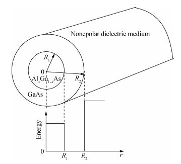
Loading [MathJax]/jax/output/HTML-CSS/jax.js
J. Semicond. > 2013, Volume 34 > Issue 4 > 042001

SEMICONDUCTOR PHYSICS

One-phonon resonant electron Raman scattering in multilayer coaxial cylindrical AlxGa1-xAs/GaAs quantum cables

Qinghu Zhong1, , Xuehua Yi1, Shouliang Pu1 and Yuzhen Yan1

+ Author Affiliations

 Corresponding author: Zhong Qinghu, Email:qhzhong05@163.com

DOI: 10.1088/1674-4926/34/4/042001

PDF

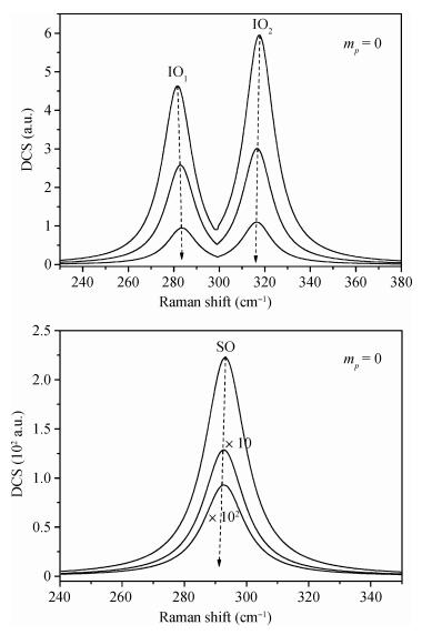
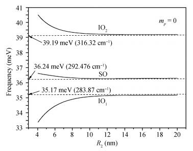
Abstract: We have presented a theoretical calculation of the differential cross section (DCS) for the electron Raman scattering (ERS) process associated with the interface optical (IO) and surface optical (SO) phonons in multilayer coaxial cylindrical AlxGa1-xAs/GaAs quantum cables (QC). We consider the Fröhlich electron-phonon interaction in the framework of the dielectric continuum approach. The selection rules for the processes are studied. Singularities are found to be sensitively size-dependent and by varying the size of the QC, it is possible to control the frequency shift in the Raman spectra. A discussion of the phonon behavior for the QC with different size is presented. The numerical results are also compared with those of experiments.

Key words: Raman scatteringoptical phonon modesquantum cables

In recent years, with the progress in semiconductor nanotechnology, such as molecular-beam epitaxy and metal-organic chemical-vapor deposition, various kinds of low-dimensional complex heterostructures can be fabricated. For example, in 1993, utilizing the method of wet chemical synthesis, Eychmüller et al.[1] synthesized spherical quantum dot quantum wells (QDQW): an inhomogeneous quantum dot (QD) with a central core barrier and several shell wells. Experimental and theoretical studies[2-7] revealed that the inner configurations for electrons and holes make many physical properties in QDQWs obviously different from those in quantum wires (QW) and QDs. In 1997 and 1998, under reactive laser ablation, inhomogeneous coaxial cylindrical quantum-well wires (QWW) were successfully synthesized by Suenaga and Zhang's group[8, 9], which were also called quantum cables (QC). Due to their peculiar properties, QC systems have attracted great attention by many authors. Zeng et al.[10] predicted the single-electron subband properties in a five-layer GaAlAs/GaAs QC system, and the systems exhibit some interesting and unique behavior unexpected in other nanostructures. Under a dielectric continuum approximation, Zhang et al.[11] study the interface optical (IO) and surface optical (SO) phonon modes, as well as the Fröhlich electron-IO (or -SO) phonon interaction Hamiltonian, in a multilayer coaxial cylindrical QC. Results revealed that the dispersion frequencies of IO or SO modes sensitively depend on small $k_{z}$ (the wavevector in the z direction) and m (the azimuthal quantum number), while for large $k_{z}$ and m, the frequency for each mode converges to the limit frequency value of the IO (or SO) mode in a single heterostructure. The phonons with higher frequencies are found to contribute more significantly to the electron-phonon interaction.

Because of its convenience and the absence of damage to the materials being measured, electron Raman scattering (ERS) has become a powerful tool to investigate different physical properties of low dimensional semiconductor systems[12-14]. Based on resonant Raman scattering, Raman injection lasers and some other opto-electronic devices can be produced[15]. Experimental research on Raman scattering in nanocrystals has been extensively reported[16-20]. Tenne et al.[21] investigate the phonon spectra of self-assembled InAs QDs in an AlAs matrix with different growth temperatures by Raman spectroscopy. The Raman spectroscopy data show that QDs grown at low temperatures appear to have smaller sizes and increasing the temperature first leads to increasing QDs size. Milekin et al.[22] studied the interface modes in InAs/Al(Ga)As QDs structures with symmetrical and asymmetrical barriers localized in the vicinity of corrugated QD/matrix and wetting layer/matrix interfaces. Results reveal that the observed interface phonon frequency positions are in good agreement with those calculated using the dielectric continuum model. To interpret experimental results, many theoretical physicists usually focus on the calculation of the differential cross section (DCS) for Raman scattering[23-26]. Thus, the calculation of the DCS for ERS remains a rather interesting and fundamental issue to achieve a better understanding of the man-made semiconductor nanostructures. Zhong et al.[27] calculate the ERS cross-section in CdS/HgS cylindrical QDQW. The rich spectra obtained in Ref. [27] provide direct information about the electron band structure. Liu et al.[28, 29] calculate the first-order Raman scattering process in quantum discs and quantum wires within the framework of dielectric continuum model. The Raman spectra they obtained give the direct information about the longitudinal optical (LO) and IO phonon respectively and have a good agreement with the experiment results.

In the present paper, we consider the Fröhlich electron-phonon interaction in the framework of the dielectric continuum model. We calculate the Raman intensity in a three-layer coaxial cylindrical Al$_{x}$Ga$_{1-x}$As/GaAs/vacuum quantum cable. Electron states are assumed to be confined within the well. Three types of optical phonons, named $\text{IO}_{1}$, $\text{IO}_{2}$ and SO modes have been investigated. The contributions of phonons to the first-order ERS are analyzed. The singularities are found to be sensitively size-dependent for small QC and by varying the size of the well it is possible to control the frequency shift in the Raman spectrum. The selection rules for the Raman scattering processes and the phonon behavior for different well size are also studied. The calculated results are compared with those of experiments.

We consider a three-layer coaxial cylindrical Al$_{x}$Ga$_{1-x}$-As/GaAs/vacuum QC system. As shown in Fig. 1, $R_{1}$, $R_{2}$ are the inner and outer radius. The electron states are considered to be confined within the well. In the envelope function approximation neglecting electron-hole Coulomb interaction the wave function for electrons can be written as

Figure  1.  The schematic structure of the three-layer coaxial cylindrical quantum cable system and its potential profile

$ ψnl(r)=C1nleilθeikzz×{Tl(βnlR1)Jl(αnlr),rR1,Jl(αnlR1)Tl(βnlr),R1<rR2,0,r>R2, $

(1)

$ Tl(βnlr)=Jl(βnlr)Jl(βnlR2)Yl(βnlR2)Yl(βnlr), $

(2)

$ C2nl=12πL[Tl(βnlR1)2R10Jl(αnlr)2rdr+Jl(βnlR1)2R2R1Tl(βnlr)2rdr], $

(3)

where $\alpha_{\rm nl}=\sqrt{2\mu_{1}(V_{\rm c}-E_{\rm nl})/\hbar^{2}}$, $\beta_{\rm nl}=\sqrt{2\mu_{2}E_{\rm nl}/\hbar^{2}}$; $J_{\rm l}$ and $Y_{l}$ are the lth-order Bessel functions of the first and second kind; $\mu_{1}$ ($\mu_{2})$ is the effective mass in the dot (well); L is the length of the QC ($L\gg R_{2}$); $C_{\rm nl}$ is the normalization factor, and $V_{\rm c}$ represents the band offset. Taking as matching boundary conditions the continuity of the function $\psi$ and the current $\partial\psi/\mu_{\rm i}\partial r$ at the interface, the energy eigenvalues $E_{\rm nl}$ are determined by the secular equation,

$ 1μ1T(βnlR1)Jl(αnlr)|r=R1=1μ2J(αnlR1)Tl(βnlr)|r=R1. $

(4)

Within the framework of the dielectric continuum approach, the Fröhlich electron-phonon interaction can be written as[11]

$ HeIO, SO=mp,qzΓIO, SOmp,qz(r)[eimpφeiqzzC+mp(qz)+H.C.], $

(5)

where

$ ΓIO, SOmp,qz(r)=Nmp,qz×{g1Imp(qzr),rR1,g2Imp(qzr)+h2Kmp(qzr),R1<rR2,Kmp(qzr),r>R2, $

(6)

and

$ |Nmp,qz|2=2ωe2kzL[(1ϵ1ϵ101ϵ1ϵ1)1×Int(1,mp,qz)+(1ϵ2ϵ201ϵ2ϵ2)1Int(2,mp,qz)]1, $

(7)

with

$ Int(1,mp,qz)=R10rdrg21[Imp1(qzr)2+Imp+1(qzr)2+2Imp(qzr)2], $

(8)

$ Int(2,mp,qz)=R10rdr[g22(Imp1(qzr)2+Imp+1(qzr)2+2Imp(qzr)2)+h22(Kmp1(qzr)2+Kmp+1(qzr)2+2Kmp(qzr)2)+2g2h2(2Imp(qzr)Kmp(qzr)+Imp1(qzr)Kmp1(qzr)Imp+1(qzr)Kmp+1(qzr))], $

(9)

$ g2=(ϵ2ϵd)Kmp(qzR2)Kmp(qzR2)[Imp(qzR2)Kmp(qzR2)Kmp(qzR2)Imp(qzR2)]ϵ2, $

(10)

$ h2=ϵ2Kmp(qzR2)Imp(qzR2)ϵdImp(qzR2)Kmp(qzR2)[Kmp(qzR2)Imp(qzR2)Imp(qzR2)Kmp(qzR2)]ϵ2, $

(11)

$ g1=g2+Kmp(qzR1)Imp(qzR1)h2, $

(12)

where $\epsilon_{\rm d}$ is the dielectric function of the vacuum.

There are different types of Raman scattering process. In this paper, we put emphasis on the three-step process (Stokes emission): in the first step, the system absorbs one $\omega_{\rm i}$ photon from the incident radiation and creates an EHP state with the electron transition from the initial state $|i\rangle$ to a virtual state $|\nu\rangle$; in the second step, the electron undergoes another transition from state $|\nu\rangle$ to another virtual state $|\mu\rangle$ and emits an optical phonon with frequency $\vartheta_{\rm p}$; in the final step, the EHP recombines with emission of a secondary-radiation photon with frequency $\omega_{\rm s}$.

The Raman cross section can be given by the third-order perturbation theory[26]

$ d2σdΩdωs=η(ωi)η3(ωs)4π23c4f|Kif|2(ωiϑp)2. $

(13)

Since the time order of quantum creation (annihilation) can be changed optionally, there are six permutations open to us, and the transition matrix elements $K_{\rm if}$ consist of six terms

$ Kifμ,νWif(μ,ν), $

(14)

with

$ Wif(μ,ν)=f|HeF(ωs)|μμ|Heph|νν|HeF(ωi)|i(ωi+EiEμϑp+jΓμ)(ωi+EiEν+jΓν)+f|HeF(ωs)|μμ|HeF(ωi)|νν|Heph|i(EiEνϑp+jΓν)(ωi+EiEμϑp+jΓμ)+f|Heph|μμ|HeF(ωs)|νν|HeF(ωi)|i(ωi+EiEν+jΓν)(EiEμϑp+jΓμ)+f|HeF(ωi)|μμ|Heph|νν|HeF(ωs)|i(EiEνωi+ϑp+jΓν)(EiEμωi+jΓμ)+f|HeF(ωi)|μμ|HeF(ωs)|νν|Heph|i(EiEμωi+jΓμ)(EiEνϑp+jΓν)+f|Heph|μμ|HeF(ωi)|νν|HeF(ωs)|i(EiEνωi+ϑp+jΓν)(EiEμϑp+jΓμ), $

(15)

where $j=\sqrt{-1}$; $\mathit{\Gamma}_{\mu}$ and $\mathit{\Gamma}_{\nu}$ are the inhomogeneous line widths of the electron transitions; $\eta(\omega)$ is the refraction index as a function of radiation frequency $\omega$; $|\nu\rangle$ and $|\mu\rangle$ denote the intermediate states with energy $\varepsilon_{\nu}$ and $\varepsilon_{\mu}$, respectively.

In the initial state $|i\rangle$ we assume a completely occupied valence band and an unoccupied conduction band, and one incident photon, so the energy $\varepsilon_{\rm i}$ for the initial state is

$ εi=ωi. $

(16)

In final state $|f\rangle$, we have a secondary-radiation emitted photon with energy $\hbar\omega_{\rm s}$, and a phonon with energy $\hbar\vartheta_{\rm p}$ and electron back to the initial state. Thus, we can get the energy $\varepsilon_{\rm f}$ for the final state,

$ εf=ωs+ϑp. $

(17)

According to the energy conservation law, we have $\varepsilon_{\rm i}=\varepsilon_{\rm f}$, hence

$ ωi=ωs+ϑp. $

(18)

For the intermediate states, the energy $\varepsilon_{\nu(\mu)}$ can be written as

$ εν=Enνlνtν+Eg, $

(19)

$ εμ=Enμlμtμ+ϑp+Eg. $

(20)

In the following, we calculate the matrix elements of the DCS in scattering configurations $Z(X, X)\overline{Z}$.

$ ν|ˆHeF(ωi)|i=jeη(ωi)2πωiΠνi, $

(21)

$ f|ˆHeF(ωs)|μ=jeη(ωs)2πωsΠμf, $

(22)

with

$ Πνi=2πLEνiCnνlνCnili[Tlν(βnνlνR1)Tli(βniliR1)×R10Jlν(αnνlνr)Jli(αnilir)r2dr+Jlν(αnνlνR1)Jli(αniliR1)×R2R1Tlν(βnνlνr)Tli(βnilir)r2dr]δlν,liδkzν,kzi, $

(23)

where

$ Eνi=EνEi, $

(24)

$E_{\mu {\rm f}}$ and $\Pi_{\mu {\rm f}}$ have similar expressions with $E_{\nu{\rm i}}$ and $\Pi_{\nu {\rm i}}$.

$ μ|ˆHIO, SOeph(ωs)|ν=ΛμνIO, SO, $

(25)

and

$ ΛμνIO, SO=2πLCnνlνCnμlμδlμ,lνlpδkzμ,kzνqz×lp,qzNlp,qz{Tlν(βnνlνR1)Tlμ(βnμlμR1)×R10Jlμ(αnμlμr)g1Imp(qzr)Jlν(αnνlνr)rdr+Jlμ(αnμlμR1)Jlν(αnνlνR1)×R2R1Tlμ(βnμlμr)[g2Imp(qzr)+h2Kmp(qzr)]×Tlν(βnνlνr)rdr}. $

(26)

The selection rules for the scattering processes are shown from Eqs. (23) to (26).

Finally, after cumbersome calculations we obtain expressions of the DCS for the three-step Raman scattering process

$ d2σdΩdωs=[d2σdΩdωs]IO+[d2σdΩdωs]SO, $

(27)

$ [d2σdΩdωs]IO, SO=e4η(ωs)(ωiϑp)23c4η(ωi)ωiωs|μ,νΥμνIO, SO|2, $

(28)

where

$ ΥμνIO, SO=ΠμfΛμνIO, SOΠνi(ωiενi+jΓν)(ωiϑpεμi+jΓμ)ΠμfΠμνΛνiIO, SO(ενi+ϑpjΓν)(ωiϑpεμi+jΓμ)ΛμfIO, SOΠμνΠμi(ωiενi+jΓν)(εμi+ϑpjΓμ)+three similar terms. $

(29)

Compared to the first three terms, the contribution of the last three terms in Eq. (28) is small enough that it can be neglected. Therefore, in the present work, we consider just the contribution of the first three terms of Eq. (28) during the calculation of $\Upsilon^{\mu\nu}_{\tau}$ for the determination of the DCS.

In this section, the resonant DCS given by Eqs. (27) and (28) is calculated numerically for a three-layer coaxial cylindrical Al$_{0.4}$Ga$_{0.6}$As/GaAs/vacuum QC. The parameters used in the computation are[30]: $\epsilon_{0}$ = 13.18, $\epsilon_{\infty}$ = 10.89, $\mu_{1}$ = 0.067$m_{0}$, $\hbar\omega_{\rm TO}$ = 33.29 meV for GaAs material and $\epsilon_{0}=12.74, \epsilon_{\infty}=10.51, \mu_{2}=0.10m_{0}, \hbar\omega_{\text{TO}}=37.63$ meV for Al$_{0.4}$Ga$_{0.6}$As material; $V_{\rm c}$ = 0.21 eV; $\Gamma_{\mu}=\Gamma_{\nu}$ = 1 meV.

In Fig. 2, under the scattering configuration $X(Z, Z)\overline{X}$, we show the DCS for the IO and SO phonons as a function of the Raman shift in a three-layer coaxial cylindrical Al$_{0.4}$Ga$_{0.6}$As/GaAs/vacuum QC. The inner radius of the QC we select here is kept at 4.0 nm and the outer radius $R_{2}=$ 8.0 nm, 10.0 nm, 12.0 nm shown by an arrow along the dash curve in the figure. Two types of IO phonons signed $\text{IO}_{1}$ and $\text{IO}_{2}$ have been investigated. From this figure, one can easily find that when increasing radius $R_{2}$, the contribution of the IO and SO phonons to the DCS decreases. However, more calculations reveal that as $R_{2}\rightarrow\infty$, for the coupling between the IO and SO phonons quickly becomes weaker and can then be considered negligible, the intensities for the IO phonons will decline to some constant while for the SO phonons, the DCS will decrease to zero. The electron-IO (SO) phonon interaction is related to the distribution of the electron wavefunction around the interface (surface). When the radius increases, the wider spacial spreading of electron wave function in the well makes its coupling with the interface phonon weaker. When $R_{2}\rightarrow\infty$, the coupling between the electron and the IO phonons will approach a constant and not depend on radius $R_{2}$, while for the SO phonons, the electron-SO phonon interaction can be negligible when radius $R_{2}$ is large enough. Moreover, the figure also shows that when increasing the radius $R_{2}$, shown in Fig. 1 by arrows, the peaks for $\text{IO}_{2}$ and $\text{SO}$ phonons are red shifted, while those for $\text{IO}_{1}$ shift to a higher frequency. However, when the radius $R_{2}$ is large enough, the peaks for both of the $\text{IO}$ and $\text{SO}$ phonons will localize at certain values, i.e., IO$_{1}$ at 283.87 cm-1, IO2 at 316.32 cm-1 and SO at 292.48 cm-1, which agrees well with the results studied by the dielectric continuum model shown in Fig. 3. This shift can be explained by the effect of size-selective Raman scattering. The effect of localization becomes significant in the small-size low dimensional systems, which results in a notable low-frequency shift of optical phonons in the QC because of their frequencies dispersion. This phenomenon tells us that by varying the size of the QC it is possible to control the frequency shift in the Raman spectrum. The same effect was also observed for various low dimensional structures by Raman scattering experiments[15-17]. Compared Fig. 2(a) with Fig. 2(b), the DCS related the SO phonons is about 2 orders smaller than that related to the IO phonons and decrease quickly as $R_{2}$ increase, thus in our models, the IO phonons make the main contribution to the Raman intensity.

Figure  2.  The Raman spectra or IO and SO phonons in a three-layer coaxial cylindrical Al$_{0.4}$Ga$_{0.6}$As/GaAs/vacuum QC with $m_{p}=0$ and scattering configuration $X(Z, Z)\overline{X}$; the inner radius is $R_{1}=4.0$ nm and the outer radius (along the arrows)$R_{2}=8.0$ nm, 10.0 nm, 12.0 nm
Figure  3.  The dispersion frequencies for the IO and SO phonons as a function of $R_{2}$ with $R_{1}= 4.0$ nm and $m_{p} = 0$

Figure 3 shows the dispersion frequencies of the IO and SO phonons as functions of the radius $R_{2}$ with $m_{p}=0$ and $R_{1}=$ 4.0 nm, which are calculated using the dielectric continuum model. This figure shows that the variation of the dispersion frequencies is obvious in small radius, while for large $R_{2}$, the value of IO and SO phonon frequency approaches certain values, respectively. From Fig. 3, we can see that the frequencies related to $\text{IO}_{2}$ and $\text{SO}$ phonons slightly decrease as $R_{2}$ rises, while for $\text{IO}_{2}$ the frequencies increase slightly. When $R_{2}\rightarrow \infty$, the Al$_{0.4}$Ga$_{0.6}$As/GaAs interface becomes a QW heterostructure[29] and the coupling between IO and SO phonons can be negligible, thus the frequencies for $\text{IO}_{1}$ and $\text{IO}_{2}$ phonons converge respectively to 35.17 meV and 39.19 meV, i.e., the frequencies of the IO phonons in QW heterostructure[29]. For the SO phonons, as $R_{2}\rightarrow \infty$, the SO phonons do not feel the curvature of the spherical surfaces[31]. Therefore, for about $R>12$ nm, the frequencies of SO phonons will converge to the limit value 36.24 meV, i.e., the frequencies of the surface optical phonons in single planar heterostructure. These results studied by the dielectric continuum model are in good accordance with the Raman spectra we have analyzed above.

In this work, we have investigated theoretically the DCS for electron Raman scattering process involving IO (SO) phonon-assisted transitions in a three-layer coaxial cylindrical Al$_{0.4}$Ga$_{0.6}$As/GaAs/vacuum QC system. Three types of optical phonons signed $\text{IO}_{1}$, $\text{IO}_{2}$ and SO have been observed. It is shown that the IO phonons make the main contribution to the DCS and as the size of the QC increase to infinity, for the coupling between the IO and SO phonons can be negligible, the contributions of the IO phonons to the DCS will become size-independent while those for the SO phonons, the DCS will decrease to zero quickly. The picks we get in the Raman spectra are sensitively radius-dependent for QC with small size. The effect of size-selective Raman scattering has been analyzed and the phonon behavior has been discussed. The frequencies for both IO and SO phonons are dispersed at small radius $R_{2}$ and converge as $R_{2}\rightarrow\infty$.


[1]
Eychmüller A, Mews A, Weller H. A quantum dot quantum well:CdS/HgS/CdS. Chem Phys Lett, 1993, 208:59 doi: 10.1016/0009-2614(93)80076-2
[2]
Mews A, Eychmüller A, Giersig M, et al. Preparation, characterization, and photophysics of the quantum dot quantum well system cadmium sulfide/mercury sulfide/cadmium sulfide. J Phys Chem, 1994, 98:934 doi: 10.1021/j100054a032
[3]
Wendler L. Hartree-Fock approximation for the quasiparticle properties of the coupled electron-phonon system in quantumwell wires in the presence of a magnetic field. Phys Rev B, 1998, 57:9214 doi: 10.1103/PhysRevB.57.9214
[4]
Wendler L. Magnetopolarons in quasi-one-dimensional quantum-well wires. Physica B, 1999, 270:172 doi: 10.1016/S0921-4526(99)00074-5
[5]
Chang K, Xia J B. Spatially separated excitons in quantum-dot quantum well structures. Phys Rev B, 1998, 57:9780 doi: 10.1103/PhysRevB.57.9780
[6]
Checchetto R, Tosello C, Miotello A, et al. Structural evolution of Fe-Al multilayer thin films for different annealing temperatures. J Phys:Condens Matter, 2001, 13:5
[7]
Assaid E, Feddi E, Khamkhami J E I, et al. Excitons in InP/InAs inhomogeneous quantum dots. J Phys:Condens Matter, 2003, 15:175 doi: 10.1088/0953-8984/15/2/317
[8]
Suenaga K, Colliex C, Demoncy N, et al. Synthesis of nanoparticles and nanotubes with well-separated layers of boron nitride and carbon. Science, 1997, 278:653 doi: 10.1126/science.278.5338.653
[9]
Zhang Y, Suenaga K, Colliex C, et al. Coaxial nanocable:silicon carbide and silicon oxide sheathed with boron nitride and carbon. Science, 1998, 281:973 doi: 10.1126/science.281.5379.973
[10]
Zeng Z Y, Xiang Y, Zhang L D. Single-particle subband structure of quantum cables. Eur J Phys B, 2000, 17:699 doi: 10.1007/s100510070111
[11]
Zhang L, Xie H J. Frohlich electron interface and surface optical R phonon interaction Hamiltonian in multilayer coaxial cylindrical AlxGa1-xAs/GaAs/GaAs quantum cables. J Phys:Condens Matter, 2003, 15:5881 doi: 10.1088/0953-8984/15/34/318
[12]
Cardona M, Güntherodt G. Light scattering in solids V. Topics in applied physics, Vol. 66, Springer, Heidelberg, 1989
[13]
Klein M V. Phonons in semiconductor superlattices. IEEE J Quantum Electron, 1986, QE-22:1760
[14]
Comas F, Trallero-Giner C, Perez-Alvarez R J. Interband-intraband electronic Raman scattering in semiconductors. J Phys C, 1986, 19:6479 doi: 10.1088/0022-3719/19/32/021
[15]
Troccoli M, Belyanin A, Capasso F, et al. Raman injection laser. Nature, 2005, 433:845 doi: 10.1038/nature03330
[16]
Krauss T D, Wise F W. Raman-scattering study of exciton-phonon coupling in PbS nanocrystals. Phys Rev B, 1997, 55:9860 doi: 10.1103/PhysRevB.55.9860
[17]
Milekhin A G, Tenne D A, Ahn D R T. Quantum dots and nanowires. In: Bandyopadhyay S, Nalwa H S. ed. Am Sci, Stevenson Ranch, Calif, 2003: 375
[18]
Zhong Q H, Sun Y T. Surface optical phonon-assisted electron Raman scattering in a free-standing quantum wire with ring geometry. Thin Solid Films, 2011, 519:8178 doi: 10.1016/j.tsf.2011.06.045
[19]
Wang D C, Zhang Y M, Zhang Y M, et al. Raman analysis of epitaxial graphene on 6H-SiC (0001) substrates under low pressure environment. Journal of Semiconductors, 2011, 32:113003 doi: 10.1088/1674-4926/32/11/113003
[20]
Zhang G J, Xiu B, Chen Y H, et al. Raman scattering of InAs quantum dots with different deposition thicknesses. Chinese Journal of Semiconductors, 2006, 27:1012
[21]
Tenne D A, Bakarov A K, Toropov A I, et al. Raman study of self-assembled InAs quantum dots embedded in AlAs:influence of growth temperature. Physica E, 2002, 13:199 doi: 10.1016/S1386-9477(01)00519-7
[22]
Milekhin A G, Toropov A I, Bakarova A K, et al. Resonant Raman scattering in nanostructures with InGaAs/AlAs quantum dots. JETP Lett, 2006, 83:83
[23]
Krauss T K, Wise F W. Raman-scattering study of excitonphonon coupling in PbS nanocrystals. Phys Rev B, 1997, 55:9860. doi: 10.1103/PhysRevB.55.9860
[24]
Sood A K, Menéndez J, Cardona M, et al. Interface vibrational modes in GaAs-AlAs superlattices. Phys Rev Lett, 1985, 54:2115 doi: 10.1103/PhysRevLett.54.2115
[25]
Hayashi S, Kanamori H. Raman scattering from the surface phonon mode in GaP microcrystals. Phys Rev B, 1982, 26:7079 doi: 10.1103/PhysRevB.26.7079
[26]
Chamberlain M P, Trallero-Giner C, Cardona M. Raman scattering from the surface phonon mode in GaP microcrystals. Phys Rev B, 1995, 51:3
[27]
Zhong Q H, Liu C H. Studies of electronic Raman scattering in CdS/HgS cylindrical quantum dot quantum well structures. Thin Solid Films, 2008, 516:3405 doi: 10.1016/j.tsf.2007.10.118
[28]
Liu C H, Ma B K, Chen C Y. Surface optical phonon-assisted electron Raman scattering in a semiconductor quantum disc. Chinese Physics, 2002, 11:7
[29]
Zhao X F, Liu C H. One phonon resonant Raman scattering in free-standing quantum wires. Physics Letters A, 2007, 364:70 doi: 10.1016/j.physleta.2006.12.070
[30]
Adachi S. GaAs, AlAs, and AlxGa1-xAs/GaAs:material parameters for use in research and device applications. J Appl Phys, 1985, 58:3
[31]
Sikorski C H, Merkt U. Spectroscopy of electronic states in InSb quantum dots. Phys Rev Lett, 1989, 62:2164 doi: 10.1103/PhysRevLett.62.2164
Fig. 1.  The schematic structure of the three-layer coaxial cylindrical quantum cable system and its potential profile

Fig. 2.  The Raman spectra or IO and SO phonons in a three-layer coaxial cylindrical Al$_{0.4}$Ga$_{0.6}$As/GaAs/vacuum QC with $m_{p}=0$ and scattering configuration $X(Z, Z)\overline{X}$; the inner radius is $R_{1}=4.0$ nm and the outer radius (along the arrows)$R_{2}=8.0$ nm, 10.0 nm, 12.0 nm

Fig. 3.  The dispersion frequencies for the IO and SO phonons as a function of $R_{2}$ with $R_{1}= 4.0$ nm and $m_{p} = 0$

[1]
Eychmüller A, Mews A, Weller H. A quantum dot quantum well:CdS/HgS/CdS. Chem Phys Lett, 1993, 208:59 doi: 10.1016/0009-2614(93)80076-2
[2]
Mews A, Eychmüller A, Giersig M, et al. Preparation, characterization, and photophysics of the quantum dot quantum well system cadmium sulfide/mercury sulfide/cadmium sulfide. J Phys Chem, 1994, 98:934 doi: 10.1021/j100054a032
[3]
Wendler L. Hartree-Fock approximation for the quasiparticle properties of the coupled electron-phonon system in quantumwell wires in the presence of a magnetic field. Phys Rev B, 1998, 57:9214 doi: 10.1103/PhysRevB.57.9214
[4]
Wendler L. Magnetopolarons in quasi-one-dimensional quantum-well wires. Physica B, 1999, 270:172 doi: 10.1016/S0921-4526(99)00074-5
[5]
Chang K, Xia J B. Spatially separated excitons in quantum-dot quantum well structures. Phys Rev B, 1998, 57:9780 doi: 10.1103/PhysRevB.57.9780
[6]
Checchetto R, Tosello C, Miotello A, et al. Structural evolution of Fe-Al multilayer thin films for different annealing temperatures. J Phys:Condens Matter, 2001, 13:5
[7]
Assaid E, Feddi E, Khamkhami J E I, et al. Excitons in InP/InAs inhomogeneous quantum dots. J Phys:Condens Matter, 2003, 15:175 doi: 10.1088/0953-8984/15/2/317
[8]
Suenaga K, Colliex C, Demoncy N, et al. Synthesis of nanoparticles and nanotubes with well-separated layers of boron nitride and carbon. Science, 1997, 278:653 doi: 10.1126/science.278.5338.653
[9]
Zhang Y, Suenaga K, Colliex C, et al. Coaxial nanocable:silicon carbide and silicon oxide sheathed with boron nitride and carbon. Science, 1998, 281:973 doi: 10.1126/science.281.5379.973
[10]
Zeng Z Y, Xiang Y, Zhang L D. Single-particle subband structure of quantum cables. Eur J Phys B, 2000, 17:699 doi: 10.1007/s100510070111
[11]
Zhang L, Xie H J. Frohlich electron interface and surface optical R phonon interaction Hamiltonian in multilayer coaxial cylindrical AlxGa1-xAs/GaAs/GaAs quantum cables. J Phys:Condens Matter, 2003, 15:5881 doi: 10.1088/0953-8984/15/34/318
[12]
Cardona M, Güntherodt G. Light scattering in solids V. Topics in applied physics, Vol. 66, Springer, Heidelberg, 1989
[13]
Klein M V. Phonons in semiconductor superlattices. IEEE J Quantum Electron, 1986, QE-22:1760
[14]
Comas F, Trallero-Giner C, Perez-Alvarez R J. Interband-intraband electronic Raman scattering in semiconductors. J Phys C, 1986, 19:6479 doi: 10.1088/0022-3719/19/32/021
[15]
Troccoli M, Belyanin A, Capasso F, et al. Raman injection laser. Nature, 2005, 433:845 doi: 10.1038/nature03330
[16]
Krauss T D, Wise F W. Raman-scattering study of exciton-phonon coupling in PbS nanocrystals. Phys Rev B, 1997, 55:9860 doi: 10.1103/PhysRevB.55.9860
[17]
Milekhin A G, Tenne D A, Ahn D R T. Quantum dots and nanowires. In: Bandyopadhyay S, Nalwa H S. ed. Am Sci, Stevenson Ranch, Calif, 2003: 375
[18]
Zhong Q H, Sun Y T. Surface optical phonon-assisted electron Raman scattering in a free-standing quantum wire with ring geometry. Thin Solid Films, 2011, 519:8178 doi: 10.1016/j.tsf.2011.06.045
[19]
Wang D C, Zhang Y M, Zhang Y M, et al. Raman analysis of epitaxial graphene on 6H-SiC (0001) substrates under low pressure environment. Journal of Semiconductors, 2011, 32:113003 doi: 10.1088/1674-4926/32/11/113003
[20]
Zhang G J, Xiu B, Chen Y H, et al. Raman scattering of InAs quantum dots with different deposition thicknesses. Chinese Journal of Semiconductors, 2006, 27:1012
[21]
Tenne D A, Bakarov A K, Toropov A I, et al. Raman study of self-assembled InAs quantum dots embedded in AlAs:influence of growth temperature. Physica E, 2002, 13:199 doi: 10.1016/S1386-9477(01)00519-7
[22]
Milekhin A G, Toropov A I, Bakarova A K, et al. Resonant Raman scattering in nanostructures with InGaAs/AlAs quantum dots. JETP Lett, 2006, 83:83
[23]
Krauss T K, Wise F W. Raman-scattering study of excitonphonon coupling in PbS nanocrystals. Phys Rev B, 1997, 55:9860. doi: 10.1103/PhysRevB.55.9860
[24]
Sood A K, Menéndez J, Cardona M, et al. Interface vibrational modes in GaAs-AlAs superlattices. Phys Rev Lett, 1985, 54:2115 doi: 10.1103/PhysRevLett.54.2115
[25]
Hayashi S, Kanamori H. Raman scattering from the surface phonon mode in GaP microcrystals. Phys Rev B, 1982, 26:7079 doi: 10.1103/PhysRevB.26.7079
[26]
Chamberlain M P, Trallero-Giner C, Cardona M. Raman scattering from the surface phonon mode in GaP microcrystals. Phys Rev B, 1995, 51:3
[27]
Zhong Q H, Liu C H. Studies of electronic Raman scattering in CdS/HgS cylindrical quantum dot quantum well structures. Thin Solid Films, 2008, 516:3405 doi: 10.1016/j.tsf.2007.10.118
[28]
Liu C H, Ma B K, Chen C Y. Surface optical phonon-assisted electron Raman scattering in a semiconductor quantum disc. Chinese Physics, 2002, 11:7
[29]
Zhao X F, Liu C H. One phonon resonant Raman scattering in free-standing quantum wires. Physics Letters A, 2007, 364:70 doi: 10.1016/j.physleta.2006.12.070
[30]
Adachi S. GaAs, AlAs, and AlxGa1-xAs/GaAs:material parameters for use in research and device applications. J Appl Phys, 1985, 58:3
[31]
Sikorski C H, Merkt U. Spectroscopy of electronic states in InSb quantum dots. Phys Rev Lett, 1989, 62:2164 doi: 10.1103/PhysRevLett.62.2164
1

Differential optical gain in a GaInN/AlGaN quantum dot

K. Jaya Bala, A. John Peter

Journal of Semiconductors, 2017, 38(6): 062001. doi: 10.1088/1674-4926/38/6/062001

2

Identification of strained black phosphorous by Raman spectroscopy

Jiawei Wan, Junhong Guo, Fangren Hu

Journal of Semiconductors, 2017, 38(4): 042003. doi: 10.1088/1674-4926/38/4/042003

3

Electro-magnetic weak coupling optical polaron and temperature effect in quantum dot

M. Tiotsop, A. J. Fotue, S. C. Kenfack, N. Issofa, A. V. Wirngo, et al.

Journal of Semiconductors, 2015, 36(10): 102001. doi: 10.1088/1674-4926/36/10/102001

4

Correlation between electrical conductivity-optical band gap energy and precursor molarities ultrasonic spray deposition of ZnO thin films

Said Benramache, Okba Belahssen, Abderrazak Guettaf, Ali Arif

Journal of Semiconductors, 2013, 34(11): 113001. doi: 10.1088/1674-4926/34/11/113001

5

Power-aware transceiver design for half-duplex bidirectional chip-to-chip optical interconnects

Jamshid Sangirov, Ikechi Augustine Ukaegbu, Gulomjon Sangirov, Tae-Woo Lee, Hyo-Hoon Park, et al.

Journal of Semiconductors, 2013, 34(12): 125001. doi: 10.1088/1674-4926/34/12/125001

6

Inter valley phonon scattering mechanism in strained Si/(101) Si1-xGex

Zhao Jin, Liping Qiao, Ce Liu, Chen Guo, Lidong Liu, et al.

Journal of Semiconductors, 2013, 34(7): 072002. doi: 10.1088/1674-4926/34/7/072002

7

Structural, electronic, magnetic and optical properties of neodymium chalcogenides using LSDA+U method

A Shankar, D P Rai, Sandeep, R K Thapa

Journal of Semiconductors, 2012, 33(8): 082001. doi: 10.1088/1674-4926/33/8/082001

8

Electron Raman scattering in a cylindrical quantum dot

Zhong Qinghu, Yi Xuehua

Journal of Semiconductors, 2012, 33(5): 052001. doi: 10.1088/1674-4926/33/5/052001

9

Optical bistability in a two-section InAs quantum-dot laser

Jiang Liwen, Ye Xiaoling, Zhou Xiaolong, Jin Peng, Lü Xueqin, et al.

Journal of Semiconductors, 2010, 31(11): 114012. doi: 10.1088/1674-4926/31/11/114012

10

Influence of optical phonons on the electronic mobility in a strained wurtzite AlN/GaN heterojunction under hydrostatic pressure

Zhou Xiaojuan, Ban Shiliang

Journal of Semiconductors, 2009, 30(8): 082001. doi: 10.1088/1674-4926/30/8/082001

11

Raman scattering studies on PZT thin films for trigonal–tetragonal phase transition

Liang Ting, Li Junhong, Du Wenlong, Xue Chenyang, Zhang Wendong, et al.

Journal of Semiconductors, 2009, 30(8): 083001. doi: 10.1088/1674-4926/30/8/083001

12

Influence of Polarization-Induced Electric Fields on Optical Properties of Intersubband Transitions in AlxGa1-xN/GaN Double Quantum Wells

Lei Shuangying, Shen Bo, Xu Fujun, Yang Zhijian, Xu Ke, et al.

Chinese Journal of Semiconductors , 2006, 27(3): 403-408.

13

Growth and Optical Properties of ZnO Films and Quantum Wells

Zhang Baoping, Kang Junyong, Yu Jinzhong, Wang Qiming, Segawa Yusaburo, et al.

Chinese Journal of Semiconductors , 2006, 27(4): 613-622.

14

30Gbit/s Parallel Optical Receiver Module

Chen Hongda, Jia Jiuchun, Pei Weihua, Tang Jun

Chinese Journal of Semiconductors , 2006, 27(4): 696-699.

15

Monte Carlo Simulation of Impurity Scattering Effect in Resonant-Phonon-Assisted Terahertz Quantum-Cascade Lasers

Cao Juncheng, Lü Jingtao

Chinese Journal of Semiconductors , 2006, 27(2): 304-308.

16

Transport Properties of Two Coupled Quantum Dots Under Optical Pumping

Ge Chuannan, Wen Jun, Peng Ju, Wang Baigeng

Chinese Journal of Semiconductors , 2006, 27(4): 598-603.

17

Polar Quasi-Confined Optical Phonon Modes in Wurtzite Quasi-One-Dimensional GaN/AlxGa1-xN Quantum Well Wires

Zhang Li

Chinese Journal of Semiconductors , 2006, 27(10): 1717-1724.

18

Resonant Raman Scattering and Photoluminescence Emissions from Above Bandgap Levels in Dilute GaAsN Alloys

Tan P H, Luo X D, Ge W K, Xu Z Y, Zhang Y, et al.

Chinese Journal of Semiconductors , 2006, 27(3): 397-402.

19

Raman Scattering of InAs Quantum Dots with Different Deposition Thicknesses

Zhang Guanjie, Xu Bo, Chen Yonghai, Yao Jianghong, Lin Yaowang, et al.

Chinese Journal of Semiconductors , 2006, 27(6): 1012-1015.

20

Temperature Dependent Raman Scattering of Phonon Modes and Defect Modes in GaN and p-Type GaN Films

Chinese Journal of Semiconductors , 2005, 26(4): 635-640.

  • Search

    Advanced Search >>

    GET CITATION

    Qinghu Zhong, Xuehua Yi, Shouliang Pu, Yuzhen Yan. One-phonon resonant electron Raman scattering in multilayer coaxial cylindrical AlxGa1-xAs/GaAs quantum cables[J]. Journal of Semiconductors, 2013, 34(4): 042001. doi: 10.1088/1674-4926/34/4/042001
    Q H Zhong, X H Yi, S L Pu, Y Z Yan. One-phonon resonant electron Raman scattering in multilayer coaxial cylindrical AlxGa1-xAs/GaAs quantum cables[J]. J. Semicond., 2013, 34(4): 042001. doi: 10.1088/1674-4926/34/4/042001.
    shu

    Export: BibTex EndNote

    Article Metrics

    Article views: 2123 Times PDF downloads: 39 Times Cited by: 0 Times

    History

    Received: 01 September 2012 Revised: 30 October 2012 Online: Published: 01 April 2013

    Catalog

      Email This Article

      User name:
      Email:*请输入正确邮箱
      Code:*验证码错误
      Qinghu Zhong, Xuehua Yi, Shouliang Pu, Yuzhen Yan. One-phonon resonant electron Raman scattering in multilayer coaxial cylindrical AlxGa1-xAs/GaAs quantum cables[J]. Journal of Semiconductors, 2013, 34(4): 042001. doi: 10.1088/1674-4926/34/4/042001 ****Q H Zhong, X H Yi, S L Pu, Y Z Yan. One-phonon resonant electron Raman scattering in multilayer coaxial cylindrical AlxGa1-xAs/GaAs quantum cables[J]. J. Semicond., 2013, 34(4): 042001. doi: 10.1088/1674-4926/34/4/042001.
      Citation:
      Qinghu Zhong, Xuehua Yi, Shouliang Pu, Yuzhen Yan. One-phonon resonant electron Raman scattering in multilayer coaxial cylindrical AlxGa1-xAs/GaAs quantum cables[J]. Journal of Semiconductors, 2013, 34(4): 042001. doi: 10.1088/1674-4926/34/4/042001 ****
      Q H Zhong, X H Yi, S L Pu, Y Z Yan. One-phonon resonant electron Raman scattering in multilayer coaxial cylindrical AlxGa1-xAs/GaAs quantum cables[J]. J. Semicond., 2013, 34(4): 042001. doi: 10.1088/1674-4926/34/4/042001.

      One-phonon resonant electron Raman scattering in multilayer coaxial cylindrical AlxGa1-xAs/GaAs quantum cables

      DOI: 10.1088/1674-4926/34/4/042001
      Funds:

      the Natural Science Foundation of Guangdong Province S2012010010976

      Project supported by the Natural Science Foundation of Guangdong Province (No. S2012010010976)

      More Information
      • Corresponding author: Zhong Qinghu, Email:qhzhong05@163.com
      • Received Date: 2012-09-01
      • Revised Date: 2012-10-30
      • Published Date: 2013-04-01

      Catalog

        /

        DownLoad:  Full-Size Img  PowerPoint
        Return
        Return