Key Laboratory of Microelectronics Devices & Integrated Technology, Institute of Microelectronics, Chinese Academy of Sciences, Beijing 100029, ChinaKey Laboratory of Microelectronics Devices & Integrated Technology, Institute of Microelectronics, Chinese Academy of Sciences, Beijing 100029, China
Abstract: Two innovative de-embedding methods are proposed for extracting an electrical model for a through-silicon-via (TSV) pair consisting of a ground-signal (GS) structure. In addition, based on microwave network theory, a new solution scheme is developed for dealing with multiple solutions of the transfer matrix during the process of de-embedding. A unique solution is determined based on the amplitude and the phase characteristic of S parameters. In the first de-embedding method, a typical "π" type model of the TSV pair is developed, which illustrates the need to allow for frequency dependence in the equivalent TSV pair Spice model. This de-embedding method is shown to be effective for extracting the electrical properties of the TSVs. The feasibility of a second de-embedding method is also investigated.
To address the miniaturization and multi functionality of electronic devices, system-in-package (3D SiP) technology, based on a silicon carrier or interposer, is rapidly gaining prominence because it offers system design flexibility, heterogeneous integration, and quick time to market[1]. The interposer generally comprises a silicon substrate with vias (TSVs) and wiring re-distribution layers (RDLs) to satisfy I/O and fan-out requirements. The interposer is an interface between the dense I/O array of a die and the less dense array of a printed circuit board (PCB). Because of the dimensional disparity between the two sets of I/Os and the length of both transmission lines and TSVs, a representative full wave simulation is expected to require multiple meshing and substantial CPU time that slows the design cycle, contrary to the requirement of a fast time-to-market. For complex three-dimensional interconnects, accurate circuit simulation models have been shown to be much more efficient for design simulation and optimization than full wave simulation models[2]. Therefore it is important to extract compact circuit model parameters for TSVs so that these may be used for efficient large scale analysis and design optimization.
The non-zero and frequency-dependent conductivity of bulk silicon and the frequency dependence of the metal-insulator-semiconductor (MIS) structure of the TSV wall both require understanding and careful circuit model construction. There are many published papers that focus on the electrical modeling of TSVs[3-7]. Cadix et al.[3] equalized TSV as a π-shaped circuit and demonstrated that TSV inductance and capacitance are 500-1000 times lower than wire bonding. Kim et al.[4] proposed a high-frequency scalable electrical model for TSV pairs (the ground-signal TSV structure) based on transmission line theory. Katti et al.[5] analyzed the closed form expression of the MIS capacitance at the TSV wall and developed an RLC model for predicting the resistance, inductance, and capacitances of small-geometry TSV architectures. Using a magneto-quasi-static theory and solutions based on a Fourier-Bessel expansion, Liu et al.[6] proposed a compact, wideband equivalent-circuit model for electrical modeling of through-silicon vias (TSVs) and studied the influence that MOS capacitance has on the signal transmission properties of TSV pairs. Xu et al.[7] introduced a comprehensive compact resistance-inductance-capacitance-conductance (RLCG) model with due considerations being given to MOS capacitance and eddy current coupling to the substrate. What is clear from the cited work is that equivalent electrical models for TSVs are evolving in an effort to account for the interaction between the TSV array and its semiconducting host. What is equally clear it that precise testing is required to verify the precision of equivalent electrical models for TSVs.
TSV structures cannot be directly probed at high frequency because of their small diameter, which can be as small as 5 μm, and because of the possibility of sample damage. Specially designed test structures are required to measure and deduce their electrical characteristics. Classical de-embedding schemes, such as those methods proposed in Refs. [8, 9], are not generally applicable because they strictly apply only to planar devices. An innovative de-embedding method specifically developed to extract buried components parameters in 3D integration is presented in Refs. [10, 11]. Using the de-embedding scheme described in Ref. [11], equivalent high frequency (HF) electrical models are extracted for the case of medium density TSV arrays with a back redistribution layer (BRDL). However, the HF de-embedding structure uses no current return path. Mong et al.[12] proposed a de-embedding method to extract the S parameters of ground-signal-ground (GSG) TSV structures but stopped short of relating the S parameters to a circuit model for the TSVs.
In this paper, two innovative de-embedding methods are proposed to extract the electrical parameters of TSV pairs. Furthermore, a solution scheme is devised to extract a unique solution for the governing ABCD matrix. Finally, matrix transformation is used to extract a unique "π" type circuit model of TSV pairs.
2.
Microwave network theory
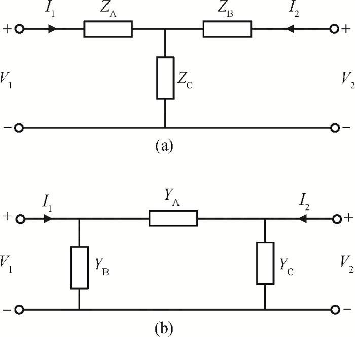
Linear two-port and multi-port networks can be represented by microwave network matrices, such as the transfer matrix (ABCD), the impedance matrix (Z), the admittance matrix (Y), and the scattering matrix (S). These matrices can be generally transformed into one another. The conversion equations for a two-port network among these matrices are shown as Eqs. (1-5). In particular, a "T"-type or "π"-type 2-port network can be conveniently represented in terms of impedance (Z) and admittance (Y) matrices whose elements are related to those of the S-matrix as shown in Eqs. (4) and (5). The transformation method is shown in Fig. 1.
Figure
1.
Equivalent circuit of a mutual two port network. (a) "T" type equivalent circuit: ZA=Z11−Z12; ZB=Z22−Z12; ZC=Z12. (b) "π" type equivalent circuit: YA=−Y12; YB=Y11+Y12; YC=Y22+Y12.
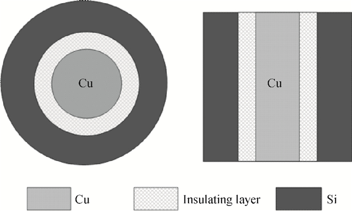
The TSV basic structure is shown in top and side views in Fig. 2. The core is generally copper and is shielded from the surrounding silicon by an insulating layer.
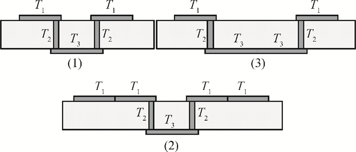
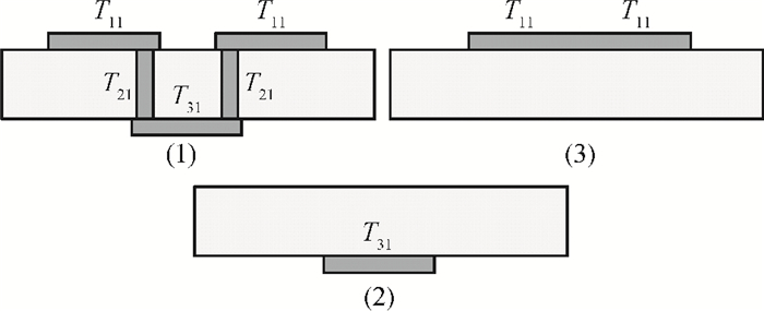
In this section, we consider as an example the TSV pair (GS). Two de-embedding structures are proposed to obtain the electrical properties of the pair. The first includes the three TSV and trace configurations shown in Fig. 3, differing only in the trace lengths of the top and bottom traces and the TSV pair separation. The variations are depicted in Fig. 3 and 4 and described in Section 3.1. The top or bottom traces are referred to as top or bottom redistribution layers (RDL). The second de-embedding structure includes a front redistribution layer (FRDL), a back redistribution layer (BRDL) as well as top and bottom RDL traces, as shown in Figs. 5 and 6 and described in Section 3.2.
Figure
3.
Top view of the first de-embedding model.
Top views and the side view of the first de-embedding model are shown as Figs. 3 and 4. Three test structures comprising two top RDL traces, a pair of TSVs, a pair of bottom RDL traces, a second pair of TSVs, and finally two top RDL traces are illustrated in the figures. The lengths of the top RDL and bottom RDL are given, respectively, by nL and mW where n, m= 1, 2. The length of the top RDL in diagram (2) is twice that in diagrams (1) or (3) and the length of the bottom RDL in diagram (3) is twice that in diagrams (1) or (2). In this way two-port measurements on separate structures can be made using a vector network analyzer to obtain the four transfer matrix elements (Tij) of the TSV pairs, (GS).
In the present case, Tm1, Tm2 and Tm3 are the transmission transfer matrices obtained from the measured S-parameters using Eq. (3). The measured S-parameters are used to generate the ABCD matrix in the beginning. Matlab can then be used to compute T1, T2 and T3, which include all the electrical properties of Top_RDL with length "L", TSV and Bottom_RDL with length "w". The impedance matrix and scattering matrix of the TSV pair are finally obtained from Eq. (4) and Eq. (1).
Tm1=T1T2T3T2T1,
(6)
Tm2=T1T1T2T3T2T1T1,
(7)
Tm3=T1T2T3T3T2T1.
(8)
3.2
A second de-embedding model
For the second de-embedding model, there are three different structures as well. The top and side views of the model are shown in Figs. 5 and 6, respectively. Different from the first model, structures (2) and (3) in the second model just comprise BRDL and FRDL portions. For structure (1), the lengths of top RDL and bottom RDL are given by L1 and W1, respectively. The length of the bottom RDL of structure (2) is the same as that in structure (1) while the length of the top RDL in structure (3) is twice that in structure (1).
Just like the first de-embedding model, Tm11, Tm21 and Tm31 are the transmission transfer matrices obtained from the measured S-parameters by using Eq. (3). Then, according to Eqs. (9), (10) and (11), Matlab can be used to compute Tm11, Tm21 and Tm31, which include all the electrical properties of the Top_RDL with length "L1", TSV and Bottom_RDL with length "w1". As in the first de-embedding model, the impedance matrix and scattering matrix of the TSV pair are obtained from Eqs. (4) and Eq. (1).
Tm11=T11⋅T21⋅T31⋅T21⋅T11,
(9)
Tm21=T31,
(10)
Tm31=T11⋅T11.
(11)
4.
Multiple solutions of the transfer matrix
4.1
Square root of a matrix
When the trace (represented by "tr") and determinant (represented by "det") of a 2 × 2 non-scalar matrix (A) satisfy the following conditions: trA2≠ 4 and detA≠ 0, there are four available values for the square root of matrix (A)[13]:
X=ϵA+ϵ1√detAItrA+2ϵ1√detA,ϵ1=±1;ϵ2=±1,
(12)
In Eq. (12) I is the identity matrix.
For the first de-embedding model, according to Eqs. (6), (7) and (8), we can obtain expressions for T1, T2 and T3.
T1=(Tm2×Tm1)1/2×(Tm1)−1,
(13)
T2=[(T1)−1×Tm1×(Tm3)−1×Tm1×(T1)−1]1/2,
(14)
T3=(T2)−1×(T1)−1×Tm1×(T1)−1×(T2)−1.
(15)
We see that there are four different solutions for T1, 16 different solutions for T2, and 64 different solutions for T3. It is too complicated to compute all the solutions and make the right choice between them. The best way is to obtain the right answer from four different square roots.
For the second de-embedding model, according to Eqs. (9), (10), and (11), we can also get expressions for T11, T21 and T31.
T11=(Tm31)1/2,
(16)
T21=(T31)−1[T31×(T11)−1×Tm11×(T11)−1]1/2,
(17)
T31=Tm21.
(18)
We see that there are four different solutions for T11 and 16 different solutions for T21. In order to simplify the matrix calculation, a method of excluding non-physical solutions must be developed.
4.2
Methods of excluding non-physical transfer matrix solutions
When dealing with the four solutions of an ABCD matrix, it is difficult to judge which is the physically correct solution for the problem. However, by observing the S parameter curves, we can easily exclude certain solutions based on amplitude and phase characteristics of S parameters. Thus, for the first de-embedding model, the four solutions of T1 are transferred into four different scattering matrices. Then the amplitude and frequency characteristics of the insertion loss (S12) are plotted and finally unphysical solutions of T1 are excluded. Calculated solutions of the transfer matrix are uniquely labeled. When ϵ1, ϵ2 in Eq. (12) are equal to 1, the corresponding solution for T1 is labeled T1(1); when ϵ2=1, ϵ2= -1, the corresponding solution is labeled T1(2); when ϵ2=−1, ϵ2=1 and ϵ2=−1, ϵ2=−1, the solutions are labeled T1(3) and T1(4), respectively. In addition, corresponding S matrices of the four solutions are correspondingly labeled S1(1), S1(2) and S1(4).
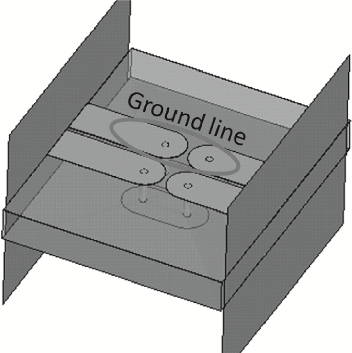
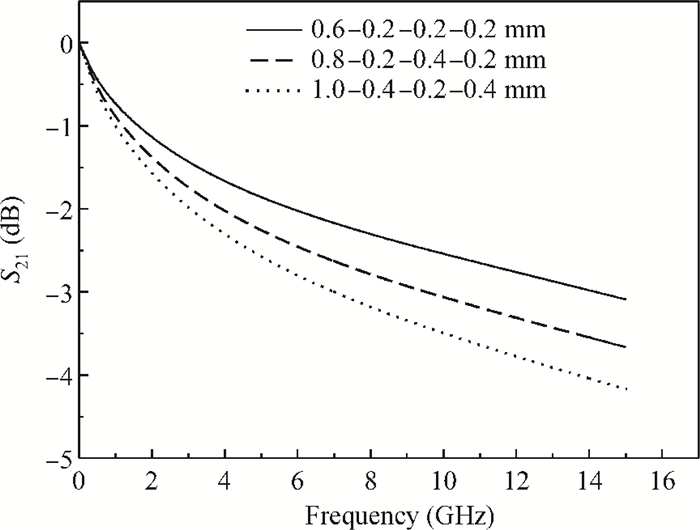
Because building the wafer with test structures is still in process, simulation results instead of test results are utilized for the time being in order to construct the Spice model. One simulation model of the first de-embedding structures is shown in Fig. 7 in which the accentuated trace is the ground line; the second is the signal line. The computed insertion loss of the first GS de-embedding structures is illustrated in Fig. 8. The label format "0.6-0.2-0.2-0.2 mm" is used to indicate a total transmission line length of 0.6 mm (2L+w= 2 × 0.2 + 0.2 = 0.6). The other similar labels have similar meanings. It is seen that the insertion loss increases with the increasing RDL length and increasing frequency, as expected. Some geometrical and material parameters pertaining to the TSVs are listed as follows: radius = 15 μm, height = 150 μm, copper filled, TSV pitch = 200 μm, thickness of the silicon dioxide insulating layer = 0.5 μm, silicon conductivity = 10 Siemens/m.
Figure
7.
One simulation model of the first de-embedding structures.
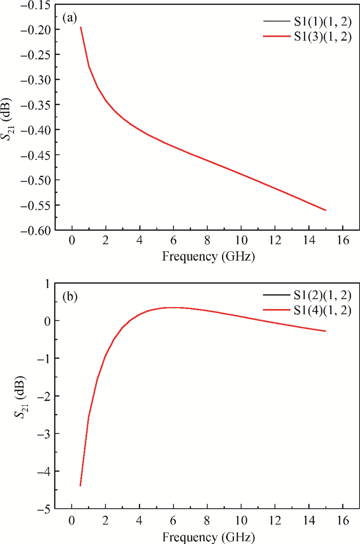
Four insertion-loss solutions for a top RDL length of (200 μm) in the first de-embedding model are shown in Fig. 9. It is seen that the insertion loss curves S1(1) and S1(3) coincide completely, as do the insertion loss curves S1(2) and S1(4). Generally, insertion loss increases with increasing frequency due to higher dielectric loss and decreasing skin depth in metal. Therefore the solutions (T1(2) and T1(4)) are excluded based on non-physical behavior; namely that the predicted insertion loss (S1(2)(1, 2) and S1(4)(1, 2)) decreases with increasing frequency. On the other hand, the two solutions (T1(1) and T1(3)), display a behavior consistent with observation and general predictions based on physical grounds.
Figure
9.
Four insertion-loss solutions for RDL length (200 μm) in the first de-embedding model. (a) S1(1) and S1(3). (b) S1(2) and S1(4).
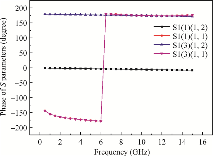
To further investigate the behavior of the transfer matrices T1(1) and T1(3), elements (Tij) of T1(1) and T1(3) were analyzed in more detail. It is found that the difference between T1(1) and T1(3) only lies in the imaginary part of elements (Tij), which explains why the corresponding amplitude frequency characteristics of the two solutions are the same (Fig. 9(a)). The imaginary part of Tij only influences the phase of S parameters. The phase curves of S1(1) and S1(3) are shown in Fig. 10. It is seen that the return-loss phases of the two solutions (S1(1)(1, 1) and S1(3)(1, 1) nearly coincide, while the insertion-loss phases of (S1(1)(1, 2) and S1(3)(1, 2) show a great difference. The relation between the imaginary part and the phase of the propagation constant of a transmission line to S21 is summarized in Eq. (19).
S12=e−γL=e−(α+jβ)L.
(19)
Figure
10.
Plot of the computed phase of S1(1) and S1(3) (Two S parameters solutions for top RDL (200 μm)).
We can determine that the phase of S21 should be minus when the RDL length is only 200 μm and the signal frequency is between 0.5 and 15 GHz. This is because the signal wavelength is much longer than the RDL length. Therefore T1(3) can be excluded as a solution and T1(1) is the right solution and ϵ1, ϵ2, in Eq. (12) should be equal to 1 when facing multiple solutions of the transfer matrix.
5.
De-embedding results of TSV pairs and analysis
5.1
Scattering matrix of TSV pairs (GS structure)
The corresponding S parameters, S2 and S21, for the TSV pairs are obtained from the transfer matrices T2 and T21 in Eq. (14) and Eq. (17), by using Eq. (1) and simple matrix transformation.
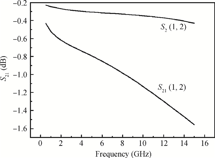
The insertion loss of TSV pairs, S2(1, 2) and S21(1, 2), obtained by the two de-embedding methods developed above, is plotted in Fig. 11. As is evident, the insertion loss predicted by different de-embedding methods can be substantially different and requires further discussion. The high loss predicted by the second de-embedding scheme may be attributed to reflection losses at discontinuous points. Referring now to Fig. 6, structure (2) (bottom RDL) and structure (3) (top RDL) are simple traces with no discontinuities, while structure (1) has four impedance discontinuities, two for each TSV.
Figure
11.
Insertion loss of TSV pairs (S2(1, 2) and S21(1, 2)) obtained by the two different de-embedding methods.
5.2
Equivalent circuit of TSV pairs (GS structure)
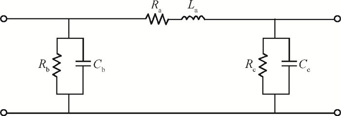
The proposed equivalent Spice model for the TSV pairs (GS) is shown in Fig. 12. It is a typical π-type circuit. There are a total of six lumped elements in this equivalent circuit.
5.2.1
Equivalent circuit of a TSV pair obtained from the first de-embedding structures
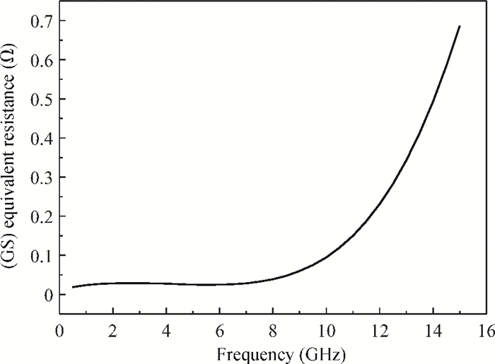
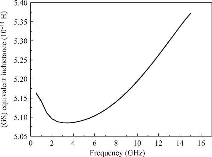
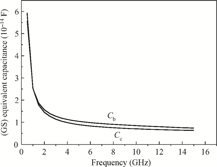
The dependence of the TSV circuit model resistance, Ra, on frequency, as calculated for the TSV pair using the first de-embedding method, is shown as Fig. 13. It is seen that when the frequency is less than 7.5 GHz, Ra is relatively stable at about 20 mΩ, and then increases rapidly with frequency due to the skin effect. Figure 14 shows the variation of the effective inductance, La, with frequency. La decreases a little to a minimum at 3 GHz, and increases thereafter showing strong frequency dependence. The equivalent inductance, La, has two contributions: TSV inductance and substrate inductance caused by eddy currents in the silicon host. The frequency dependence of the silicon substrate resistance Rb, Rc, and via capacitance Cb, Cc, as defined in the equivalent circuit in Fig. 12, are shown as Figs. 15 and 16, respectively. One should expect that Rb and Rc and Cb and Cc should be equal because of their symmetric positions. It is found that both Rb & Ra and Cb & Cc have similar trends, but have some minute differences in value, which may be caused by cumulative errors in the numerical calculation. The equivalent capacitance Cb & Cc is a combined effect of dielectric-layer capacitance, MOS capacitance and substrate capacitance. As is seen in Fig. 15, the capacitance decreases substantially between 0.5 to 2 GHz, and becomes stable thereafter, at about 10 fF. It can be concluded that the equivalent capacitance, Cc and Cb, and TSV resistance (Ra) may be taken as constants for frequencies between 2 and 8 GHz, while other lumped-element values depend on frequency. Our calculated values are very close to those reported by other works[3-7], demonstrating that the proposed method for extracting electrical parameters, though simple, is effective, the caveat being that the equivalent Spice model must allow for frequency dependence.
Figure
13.
Frequency dependence of Ra obtained in the first de-embedding model.
5.2.2
Equivalent circuit for a TSV pair obtained by the second de-embedding structures
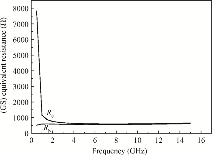
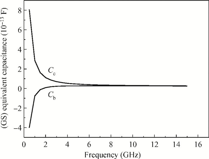
For the second de-embedding method, we were unsuccessful in obtaining "T"-type or "π"-type circuit models. In the case of a "T"-type circuit, both the lumped capacitance and resistance seem to diverge at low frequencies. The resistance of silicon substrate Rb, Rc, and via capacitance Cb, Cc, as defined in the equivalent circuit in Fig. 12, are shown as Figs. 17 and 18, respectively. As discussed previously, both resistance Rb and Rc and capacitance Cb and Cc should be equal because of their symmetric positions, however, both Rb and Rc and Cb and Cc show diverging behavior at < 4 GHz. The intent was to remove the influence of the RDL in the second de-embedding scheme by de-embedding structures (2) and (3), which should behave like a calibration trace on a silicon surface. Then the circuit behavior of the TSV would be obtained by de-embedding structure (1). The reasoning appears to be sound but the low frequency results are difficult to explain. Work continues.
Figure
17.
Frequency dependence of Rb, Rc (2nd de-embedding model).
In this paper, two innovative de-embedding methods are proposed to extract electrical models of TSV pairs (signal-ground structure) based on microwave network theory. In addition, a new solution scheme is put forward to handle multiple solutions of the transfer matrix, which considers the amplitude and phase characteristic of the S parameters as a way of eliminating non-physical solutions. Based on the first de-embedding method, a typical "π" type model of TSV pairs is obtained and illustrates the need to include the frequency dependence of both via and host substrate in an equivalent Spice model of TSVs. The first de-embedding method is shown to be capable of extracting electrical properties of TSVs. A second de-embedding method, while based on a reasonable argument, shows unexpected behavior at low frequencies and needs additional development.
References
[1]
Zhou J, Wan L, Dai F, et al. Accurate electrical simulation and design optimization for silicon interposer considering the MOS effect and eddy currents in the silicon substrate. Proc 63th Electronic Components and Technology Conference, 2012:658 http://ieeexplore.ieee.org/document/6248902/?arnumber=6248902&punumber%3D6241679
[2]
Kamgaing T, Elsherbini A, Rao V. Design acceleration of embedding RF inductors on a multilayer flip chip package substrate. Proc 62th Electronic Components and Technology Conference, 2010:133 http://ieeexplore.ieee.org/document/5898503/authors
[3]
Cadix L, Bermond C, Fuchs C, et al. RF characterization and modelling of high density through silicon vias for 3D chip stacking. Microelectron Eng, 2010, 87:491 doi: 10.1016/j.mee.2009.08.026
[4]
Kim J, Pak J S, Cho J, et al. High-frequency scalable electrical model and analysis of a through silicon via (TSV). IEEE Trans Comp Packag Manuf Technol, 2011, 1(2):181 doi: 10.1109/TCPMT.2010.2101890
[5]
Katti G, Stucchi M, Meyer K D, et al. Electrical modeling and characterization of through silicon via for three-dimensional ICs. IEEE Trans Electron Devices, 2010, 57(1):256 doi: 10.1109/TED.2009.2034508
[6]
Liu E X, Li E P, Ewe W B, et al. Compact wideband equivalent-circuit model for electrical modeling of through-silicon via. IEEE Trans Microw Theory Tech, 2011, 59(6):1454 doi: 10.1109/TMTT.2011.2116039
Vandamme E P, Schreurs D M M P, van Dinther C. Improved three-step de-embedding method to accurately account for the influence of pad parasitics in silicon on-wafer RF test-structures. IEEE Tran Electron Devices, 2001, 48(4):737 doi: 10.1109/16.915712
[9]
Tiemeijer L F, Havens R J, Jansman A B M, et al. Comparison of the "pad-open-short" and "open-short-load" deembedding techniques for accurate on-wafer RF characterization of high-quality passives. IEEE Trans Microw Theory Tech, 2005, 53(2):723 doi: 10.1109/TMTT.2004.840621
[10]
Fourneaud L, Lacrevaz T, Charbonnier J. Innovative HF extraction procedure of the characteristic impedance for embedding planar transmission line on high conductive Si substrate. Proc Asia-Pacific Microwave Conference, 2010:606 http://ieeexplore.ieee.org/document/5728364/
[11]
Fourneaud L, Lacrevaz T, Charbonnier J, et al. Extraction of equivalent high frequency models for TSV and RDL interconnects embedding in stacks of the 3D integration technology. 15th IEEE Workshop on Digital Object Identifier Signal Propagation on Interconnects (SPI), 2011:61 http://ieeexplore.ieee.org/document/5898841/authors
Fig. 1.
Equivalent circuit of a mutual two port network. (a) "T" type equivalent circuit: ZA=Z11−Z12; ZB=Z22−Z12; ZC=Z12. (b) "π" type equivalent circuit: YA=−Y12; YB=Y11+Y12; YC=Y22+Y12.
Zhou J, Wan L, Dai F, et al. Accurate electrical simulation and design optimization for silicon interposer considering the MOS effect and eddy currents in the silicon substrate. Proc 63th Electronic Components and Technology Conference, 2012:658 http://ieeexplore.ieee.org/document/6248902/?arnumber=6248902&punumber%3D6241679
[2]
Kamgaing T, Elsherbini A, Rao V. Design acceleration of embedding RF inductors on a multilayer flip chip package substrate. Proc 62th Electronic Components and Technology Conference, 2010:133 http://ieeexplore.ieee.org/document/5898503/authors
[3]
Cadix L, Bermond C, Fuchs C, et al. RF characterization and modelling of high density through silicon vias for 3D chip stacking. Microelectron Eng, 2010, 87:491 doi: 10.1016/j.mee.2009.08.026
[4]
Kim J, Pak J S, Cho J, et al. High-frequency scalable electrical model and analysis of a through silicon via (TSV). IEEE Trans Comp Packag Manuf Technol, 2011, 1(2):181 doi: 10.1109/TCPMT.2010.2101890
[5]
Katti G, Stucchi M, Meyer K D, et al. Electrical modeling and characterization of through silicon via for three-dimensional ICs. IEEE Trans Electron Devices, 2010, 57(1):256 doi: 10.1109/TED.2009.2034508
[6]
Liu E X, Li E P, Ewe W B, et al. Compact wideband equivalent-circuit model for electrical modeling of through-silicon via. IEEE Trans Microw Theory Tech, 2011, 59(6):1454 doi: 10.1109/TMTT.2011.2116039
Vandamme E P, Schreurs D M M P, van Dinther C. Improved three-step de-embedding method to accurately account for the influence of pad parasitics in silicon on-wafer RF test-structures. IEEE Tran Electron Devices, 2001, 48(4):737 doi: 10.1109/16.915712
[9]
Tiemeijer L F, Havens R J, Jansman A B M, et al. Comparison of the "pad-open-short" and "open-short-load" deembedding techniques for accurate on-wafer RF characterization of high-quality passives. IEEE Trans Microw Theory Tech, 2005, 53(2):723 doi: 10.1109/TMTT.2004.840621
[10]
Fourneaud L, Lacrevaz T, Charbonnier J. Innovative HF extraction procedure of the characteristic impedance for embedding planar transmission line on high conductive Si substrate. Proc Asia-Pacific Microwave Conference, 2010:606 http://ieeexplore.ieee.org/document/5728364/
[11]
Fourneaud L, Lacrevaz T, Charbonnier J, et al. Extraction of equivalent high frequency models for TSV and RDL interconnects embedding in stacks of the 3D integration technology. 15th IEEE Workshop on Digital Object Identifier Signal Propagation on Interconnects (SPI), 2011:61 http://ieeexplore.ieee.org/document/5898841/authors
Chinese Journal of Semiconductors , 2005, 26(11): 2058-2061.
Search
GET CITATION
Jing Zhou, Lixi Wan, Jun Li, Huijuan Wang, Fengwei Dai, Daniel Guidotti, Liqiang Cao, Daquan Yu. New de-embedding structures for extracting the electrical parameters of a through-silicon-via pair[J]. Journal of Semiconductors, 2013, 34(4): 045004. doi: 10.1088/1674-4926/34/4/045004
J Zhou, L X Wan, J Li, H J Wang, F W Dai, D Guidotti, L Q Cao, D Q Yu. New de-embedding structures for extracting the electrical parameters of a through-silicon-via pair[J]. J. Semicond., 2013, 34(4): 045004. doi: 10.1088/1674-4926/34/4/045004.
Export: BibTexEndNote
Share:
Article Metrics
Article views: 2536 TimesPDF downloads: 29 TimesCited by: 0 Times
History
Received: 18 August 2012Revised: 07 October 2012Online:Published: 01 April 2013
Jing Zhou, Lixi Wan, Jun Li, Huijuan Wang, Fengwei Dai, Daniel Guidotti, Liqiang Cao, Daquan Yu. New de-embedding structures for extracting the electrical parameters of a through-silicon-via pair[J]. Journal of Semiconductors, 2013, 34(4): 045004. doi: 10.1088/1674-4926/34/4/045004 ****J Zhou, L X Wan, J Li, H J Wang, F W Dai, D Guidotti, L Q Cao, D Q Yu. New de-embedding structures for extracting the electrical parameters of a through-silicon-via pair[J]. J. Semicond., 2013, 34(4): 045004. doi: 10.1088/1674-4926/34/4/045004.
Citation:
Jing Zhou, Lixi Wan, Jun Li, Huijuan Wang, Fengwei Dai, Daniel Guidotti, Liqiang Cao, Daquan Yu. New de-embedding structures for extracting the electrical parameters of a through-silicon-via pair[J]. Journal of Semiconductors, 2013, 34(4): 045004. doi: 10.1088/1674-4926/34/4/045004
****
J Zhou, L X Wan, J Li, H J Wang, F W Dai, D Guidotti, L Q Cao, D Q Yu. New de-embedding structures for extracting the electrical parameters of a through-silicon-via pair[J]. J. Semicond., 2013, 34(4): 045004. doi: 10.1088/1674-4926/34/4/045004.
Key Laboratory of Microelectronics Devices & Integrated Technology, Institute of Microelectronics, Chinese Academy of Sciences, Beijing 100029, China
Funds:
Project supported by the Opening Project of Key Laboratory of Microelectronics Devices & Integrated Technology, Institute of Microelectronics, Chinese Academy of Sciences. Yu Daquan also appreciates the support by 100 Talents Program (No.Y0YB049001) of Chinese Academy of Sciences
Yu Daquan also appreciates the support by 100 Talents Program of Chinese Academy of SciencesY0YB049001
the Opening Project of Key Laboratory of Microelectronics Devices & Integrated Technology
Institute of Microelectronics, Chinese Academy of Sciences
Two innovative de-embedding methods are proposed for extracting an electrical model for a through-silicon-via (TSV) pair consisting of a ground-signal (GS) structure. In addition, based on microwave network theory, a new solution scheme is developed for dealing with multiple solutions of the transfer matrix during the process of de-embedding. A unique solution is determined based on the amplitude and the phase characteristic of S parameters. In the first de-embedding method, a typical "π" type model of the TSV pair is developed, which illustrates the need to allow for frequency dependence in the equivalent TSV pair Spice model. This de-embedding method is shown to be effective for extracting the electrical properties of the TSVs. The feasibility of a second de-embedding method is also investigated.
To address the miniaturization and multi functionality of electronic devices, system-in-package (3D SiP) technology, based on a silicon carrier or interposer, is rapidly gaining prominence because it offers system design flexibility, heterogeneous integration, and quick time to market[1]. The interposer generally comprises a silicon substrate with vias (TSVs) and wiring re-distribution layers (RDLs) to satisfy I/O and fan-out requirements. The interposer is an interface between the dense I/O array of a die and the less dense array of a printed circuit board (PCB). Because of the dimensional disparity between the two sets of I/Os and the length of both transmission lines and TSVs, a representative full wave simulation is expected to require multiple meshing and substantial CPU time that slows the design cycle, contrary to the requirement of a fast time-to-market. For complex three-dimensional interconnects, accurate circuit simulation models have been shown to be much more efficient for design simulation and optimization than full wave simulation models[2]. Therefore it is important to extract compact circuit model parameters for TSVs so that these may be used for efficient large scale analysis and design optimization.
The non-zero and frequency-dependent conductivity of bulk silicon and the frequency dependence of the metal-insulator-semiconductor (MIS) structure of the TSV wall both require understanding and careful circuit model construction. There are many published papers that focus on the electrical modeling of TSVs[3-7]. Cadix et al.[3] equalized TSV as a π-shaped circuit and demonstrated that TSV inductance and capacitance are 500-1000 times lower than wire bonding. Kim et al.[4] proposed a high-frequency scalable electrical model for TSV pairs (the ground-signal TSV structure) based on transmission line theory. Katti et al.[5] analyzed the closed form expression of the MIS capacitance at the TSV wall and developed an RLC model for predicting the resistance, inductance, and capacitances of small-geometry TSV architectures. Using a magneto-quasi-static theory and solutions based on a Fourier-Bessel expansion, Liu et al.[6] proposed a compact, wideband equivalent-circuit model for electrical modeling of through-silicon vias (TSVs) and studied the influence that MOS capacitance has on the signal transmission properties of TSV pairs. Xu et al.[7] introduced a comprehensive compact resistance-inductance-capacitance-conductance (RLCG) model with due considerations being given to MOS capacitance and eddy current coupling to the substrate. What is clear from the cited work is that equivalent electrical models for TSVs are evolving in an effort to account for the interaction between the TSV array and its semiconducting host. What is equally clear it that precise testing is required to verify the precision of equivalent electrical models for TSVs.
TSV structures cannot be directly probed at high frequency because of their small diameter, which can be as small as 5 μm, and because of the possibility of sample damage. Specially designed test structures are required to measure and deduce their electrical characteristics. Classical de-embedding schemes, such as those methods proposed in Refs. [8, 9], are not generally applicable because they strictly apply only to planar devices. An innovative de-embedding method specifically developed to extract buried components parameters in 3D integration is presented in Refs. [10, 11]. Using the de-embedding scheme described in Ref. [11], equivalent high frequency (HF) electrical models are extracted for the case of medium density TSV arrays with a back redistribution layer (BRDL). However, the HF de-embedding structure uses no current return path. Mong et al.[12] proposed a de-embedding method to extract the S parameters of ground-signal-ground (GSG) TSV structures but stopped short of relating the S parameters to a circuit model for the TSVs.
In this paper, two innovative de-embedding methods are proposed to extract the electrical parameters of TSV pairs. Furthermore, a solution scheme is devised to extract a unique solution for the governing ABCD matrix. Finally, matrix transformation is used to extract a unique "π" type circuit model of TSV pairs.
2.
Microwave network theory
Linear two-port and multi-port networks can be represented by microwave network matrices, such as the transfer matrix (ABCD), the impedance matrix (Z), the admittance matrix (Y), and the scattering matrix (S). These matrices can be generally transformed into one another. The conversion equations for a two-port network among these matrices are shown as Eqs. (1-5). In particular, a "T"-type or "π"-type 2-port network can be conveniently represented in terms of impedance (Z) and admittance (Y) matrices whose elements are related to those of the S-matrix as shown in Eqs. (4) and (5). The transformation method is shown in Fig. 1.
Figure
1.
Equivalent circuit of a mutual two port network. (a) "T" type equivalent circuit: ZA=Z11−Z12; ZB=Z22−Z12; ZC=Z12. (b) "π" type equivalent circuit: YA=−Y12; YB=Y11+Y12; YC=Y22+Y12.
The TSV basic structure is shown in top and side views in Fig. 2. The core is generally copper and is shielded from the surrounding silicon by an insulating layer.
In this section, we consider as an example the TSV pair (GS). Two de-embedding structures are proposed to obtain the electrical properties of the pair. The first includes the three TSV and trace configurations shown in Fig. 3, differing only in the trace lengths of the top and bottom traces and the TSV pair separation. The variations are depicted in Fig. 3 and 4 and described in Section 3.1. The top or bottom traces are referred to as top or bottom redistribution layers (RDL). The second de-embedding structure includes a front redistribution layer (FRDL), a back redistribution layer (BRDL) as well as top and bottom RDL traces, as shown in Figs. 5 and 6 and described in Section 3.2.
Figure
3.
Top view of the first de-embedding model.
Top views and the side view of the first de-embedding model are shown as Figs. 3 and 4. Three test structures comprising two top RDL traces, a pair of TSVs, a pair of bottom RDL traces, a second pair of TSVs, and finally two top RDL traces are illustrated in the figures. The lengths of the top RDL and bottom RDL are given, respectively, by nL and mW where n, m= 1, 2. The length of the top RDL in diagram (2) is twice that in diagrams (1) or (3) and the length of the bottom RDL in diagram (3) is twice that in diagrams (1) or (2). In this way two-port measurements on separate structures can be made using a vector network analyzer to obtain the four transfer matrix elements (Tij) of the TSV pairs, (GS).
In the present case, Tm1, Tm2 and Tm3 are the transmission transfer matrices obtained from the measured S-parameters using Eq. (3). The measured S-parameters are used to generate the ABCD matrix in the beginning. Matlab can then be used to compute T1, T2 and T3, which include all the electrical properties of Top_RDL with length "L", TSV and Bottom_RDL with length "w". The impedance matrix and scattering matrix of the TSV pair are finally obtained from Eq. (4) and Eq. (1).
Tm1=T1T2T3T2T1,
(6)
Tm2=T1T1T2T3T2T1T1,
(7)
Tm3=T1T2T3T3T2T1.
(8)
3.2
A second de-embedding model
For the second de-embedding model, there are three different structures as well. The top and side views of the model are shown in Figs. 5 and 6, respectively. Different from the first model, structures (2) and (3) in the second model just comprise BRDL and FRDL portions. For structure (1), the lengths of top RDL and bottom RDL are given by L1 and W1, respectively. The length of the bottom RDL of structure (2) is the same as that in structure (1) while the length of the top RDL in structure (3) is twice that in structure (1).
Just like the first de-embedding model, Tm11, Tm21 and Tm31 are the transmission transfer matrices obtained from the measured S-parameters by using Eq. (3). Then, according to Eqs. (9), (10) and (11), Matlab can be used to compute Tm11, Tm21 and Tm31, which include all the electrical properties of the Top_RDL with length "L1", TSV and Bottom_RDL with length "w1". As in the first de-embedding model, the impedance matrix and scattering matrix of the TSV pair are obtained from Eqs. (4) and Eq. (1).
Tm11=T11⋅T21⋅T31⋅T21⋅T11,
(9)
Tm21=T31,
(10)
Tm31=T11⋅T11.
(11)
4.
Multiple solutions of the transfer matrix
4.1
Square root of a matrix
When the trace (represented by "tr") and determinant (represented by "det") of a 2 × 2 non-scalar matrix (A) satisfy the following conditions: trA2≠ 4 and detA≠ 0, there are four available values for the square root of matrix (A)[13]:
X=ϵA+ϵ1√detAItrA+2ϵ1√detA,ϵ1=±1;ϵ2=±1,
(12)
In Eq. (12) I is the identity matrix.
For the first de-embedding model, according to Eqs. (6), (7) and (8), we can obtain expressions for T1, T2 and T3.
T1=(Tm2×Tm1)1/2×(Tm1)−1,
(13)
T2=[(T1)−1×Tm1×(Tm3)−1×Tm1×(T1)−1]1/2,
(14)
T3=(T2)−1×(T1)−1×Tm1×(T1)−1×(T2)−1.
(15)
We see that there are four different solutions for T1, 16 different solutions for T2, and 64 different solutions for T3. It is too complicated to compute all the solutions and make the right choice between them. The best way is to obtain the right answer from four different square roots.
For the second de-embedding model, according to Eqs. (9), (10), and (11), we can also get expressions for T11, T21 and T31.
T11=(Tm31)1/2,
(16)
T21=(T31)−1[T31×(T11)−1×Tm11×(T11)−1]1/2,
(17)
T31=Tm21.
(18)
We see that there are four different solutions for T11 and 16 different solutions for T21. In order to simplify the matrix calculation, a method of excluding non-physical solutions must be developed.
4.2
Methods of excluding non-physical transfer matrix solutions
When dealing with the four solutions of an ABCD matrix, it is difficult to judge which is the physically correct solution for the problem. However, by observing the S parameter curves, we can easily exclude certain solutions based on amplitude and phase characteristics of S parameters. Thus, for the first de-embedding model, the four solutions of T1 are transferred into four different scattering matrices. Then the amplitude and frequency characteristics of the insertion loss (S12) are plotted and finally unphysical solutions of T1 are excluded. Calculated solutions of the transfer matrix are uniquely labeled. When ϵ1, ϵ2 in Eq. (12) are equal to 1, the corresponding solution for T1 is labeled T1(1); when ϵ2=1, ϵ2= -1, the corresponding solution is labeled T1(2); when ϵ2=−1, ϵ2=1 and ϵ2=−1, ϵ2=−1, the solutions are labeled T1(3) and T1(4), respectively. In addition, corresponding S matrices of the four solutions are correspondingly labeled S1(1), S1(2) and S1(4).
Because building the wafer with test structures is still in process, simulation results instead of test results are utilized for the time being in order to construct the Spice model. One simulation model of the first de-embedding structures is shown in Fig. 7 in which the accentuated trace is the ground line; the second is the signal line. The computed insertion loss of the first GS de-embedding structures is illustrated in Fig. 8. The label format "0.6-0.2-0.2-0.2 mm" is used to indicate a total transmission line length of 0.6 mm (2L+w= 2 × 0.2 + 0.2 = 0.6). The other similar labels have similar meanings. It is seen that the insertion loss increases with the increasing RDL length and increasing frequency, as expected. Some geometrical and material parameters pertaining to the TSVs are listed as follows: radius = 15 μm, height = 150 μm, copper filled, TSV pitch = 200 μm, thickness of the silicon dioxide insulating layer = 0.5 μm, silicon conductivity = 10 Siemens/m.
Figure
7.
One simulation model of the first de-embedding structures.
Four insertion-loss solutions for a top RDL length of (200 μm) in the first de-embedding model are shown in Fig. 9. It is seen that the insertion loss curves S1(1) and S1(3) coincide completely, as do the insertion loss curves S1(2) and S1(4). Generally, insertion loss increases with increasing frequency due to higher dielectric loss and decreasing skin depth in metal. Therefore the solutions (T1(2) and T1(4)) are excluded based on non-physical behavior; namely that the predicted insertion loss (S1(2)(1, 2) and S1(4)(1, 2)) decreases with increasing frequency. On the other hand, the two solutions (T1(1) and T1(3)), display a behavior consistent with observation and general predictions based on physical grounds.
Figure
9.
Four insertion-loss solutions for RDL length (200 μm) in the first de-embedding model. (a) S1(1) and S1(3). (b) S1(2) and S1(4).
To further investigate the behavior of the transfer matrices T1(1) and T1(3), elements (Tij) of T1(1) and T1(3) were analyzed in more detail. It is found that the difference between T1(1) and T1(3) only lies in the imaginary part of elements (Tij), which explains why the corresponding amplitude frequency characteristics of the two solutions are the same (Fig. 9(a)). The imaginary part of Tij only influences the phase of S parameters. The phase curves of S1(1) and S1(3) are shown in Fig. 10. It is seen that the return-loss phases of the two solutions (S1(1)(1, 1) and S1(3)(1, 1) nearly coincide, while the insertion-loss phases of (S1(1)(1, 2) and S1(3)(1, 2) show a great difference. The relation between the imaginary part and the phase of the propagation constant of a transmission line to S21 is summarized in Eq. (19).
S12=e−γL=e−(α+jβ)L.
(19)
Figure
10.
Plot of the computed phase of S1(1) and S1(3) (Two S parameters solutions for top RDL (200 μm)).
We can determine that the phase of S21 should be minus when the RDL length is only 200 μm and the signal frequency is between 0.5 and 15 GHz. This is because the signal wavelength is much longer than the RDL length. Therefore T1(3) can be excluded as a solution and T1(1) is the right solution and ϵ1, ϵ2, in Eq. (12) should be equal to 1 when facing multiple solutions of the transfer matrix.
5.
De-embedding results of TSV pairs and analysis
5.1
Scattering matrix of TSV pairs (GS structure)
The corresponding S parameters, S2 and S21, for the TSV pairs are obtained from the transfer matrices T2 and T21 in Eq. (14) and Eq. (17), by using Eq. (1) and simple matrix transformation.
The insertion loss of TSV pairs, S2(1, 2) and S21(1, 2), obtained by the two de-embedding methods developed above, is plotted in Fig. 11. As is evident, the insertion loss predicted by different de-embedding methods can be substantially different and requires further discussion. The high loss predicted by the second de-embedding scheme may be attributed to reflection losses at discontinuous points. Referring now to Fig. 6, structure (2) (bottom RDL) and structure (3) (top RDL) are simple traces with no discontinuities, while structure (1) has four impedance discontinuities, two for each TSV.
Figure
11.
Insertion loss of TSV pairs (S2(1, 2) and S21(1, 2)) obtained by the two different de-embedding methods.
5.2
Equivalent circuit of TSV pairs (GS structure)
The proposed equivalent Spice model for the TSV pairs (GS) is shown in Fig. 12. It is a typical π-type circuit. There are a total of six lumped elements in this equivalent circuit.
5.2.1
Equivalent circuit of a TSV pair obtained from the first de-embedding structures
The dependence of the TSV circuit model resistance, Ra, on frequency, as calculated for the TSV pair using the first de-embedding method, is shown as Fig. 13. It is seen that when the frequency is less than 7.5 GHz, Ra is relatively stable at about 20 mΩ, and then increases rapidly with frequency due to the skin effect. Figure 14 shows the variation of the effective inductance, La, with frequency. La decreases a little to a minimum at 3 GHz, and increases thereafter showing strong frequency dependence. The equivalent inductance, La, has two contributions: TSV inductance and substrate inductance caused by eddy currents in the silicon host. The frequency dependence of the silicon substrate resistance Rb, Rc, and via capacitance Cb, Cc, as defined in the equivalent circuit in Fig. 12, are shown as Figs. 15 and 16, respectively. One should expect that Rb and Rc and Cb and Cc should be equal because of their symmetric positions. It is found that both Rb & Ra and Cb & Cc have similar trends, but have some minute differences in value, which may be caused by cumulative errors in the numerical calculation. The equivalent capacitance Cb & Cc is a combined effect of dielectric-layer capacitance, MOS capacitance and substrate capacitance. As is seen in Fig. 15, the capacitance decreases substantially between 0.5 to 2 GHz, and becomes stable thereafter, at about 10 fF. It can be concluded that the equivalent capacitance, Cc and Cb, and TSV resistance (Ra) may be taken as constants for frequencies between 2 and 8 GHz, while other lumped-element values depend on frequency. Our calculated values are very close to those reported by other works[3-7], demonstrating that the proposed method for extracting electrical parameters, though simple, is effective, the caveat being that the equivalent Spice model must allow for frequency dependence.
Figure
13.
Frequency dependence of Ra obtained in the first de-embedding model.
5.2.2
Equivalent circuit for a TSV pair obtained by the second de-embedding structures
For the second de-embedding method, we were unsuccessful in obtaining "T"-type or "π"-type circuit models. In the case of a "T"-type circuit, both the lumped capacitance and resistance seem to diverge at low frequencies. The resistance of silicon substrate Rb, Rc, and via capacitance Cb, Cc, as defined in the equivalent circuit in Fig. 12, are shown as Figs. 17 and 18, respectively. As discussed previously, both resistance Rb and Rc and capacitance Cb and Cc should be equal because of their symmetric positions, however, both Rb and Rc and Cb and Cc show diverging behavior at < 4 GHz. The intent was to remove the influence of the RDL in the second de-embedding scheme by de-embedding structures (2) and (3), which should behave like a calibration trace on a silicon surface. Then the circuit behavior of the TSV would be obtained by de-embedding structure (1). The reasoning appears to be sound but the low frequency results are difficult to explain. Work continues.
Figure
17.
Frequency dependence of Rb, Rc (2nd de-embedding model).
In this paper, two innovative de-embedding methods are proposed to extract electrical models of TSV pairs (signal-ground structure) based on microwave network theory. In addition, a new solution scheme is put forward to handle multiple solutions of the transfer matrix, which considers the amplitude and phase characteristic of the S parameters as a way of eliminating non-physical solutions. Based on the first de-embedding method, a typical "π" type model of TSV pairs is obtained and illustrates the need to include the frequency dependence of both via and host substrate in an equivalent Spice model of TSVs. The first de-embedding method is shown to be capable of extracting electrical properties of TSVs. A second de-embedding method, while based on a reasonable argument, shows unexpected behavior at low frequencies and needs additional development.
Zhou J, Wan L, Dai F, et al. Accurate electrical simulation and design optimization for silicon interposer considering the MOS effect and eddy currents in the silicon substrate. Proc 63th Electronic Components and Technology Conference, 2012:658 http://ieeexplore.ieee.org/document/6248902/?arnumber=6248902&punumber%3D6241679
[2]
Kamgaing T, Elsherbini A, Rao V. Design acceleration of embedding RF inductors on a multilayer flip chip package substrate. Proc 62th Electronic Components and Technology Conference, 2010:133 http://ieeexplore.ieee.org/document/5898503/authors
[3]
Cadix L, Bermond C, Fuchs C, et al. RF characterization and modelling of high density through silicon vias for 3D chip stacking. Microelectron Eng, 2010, 87:491 doi: 10.1016/j.mee.2009.08.026
[4]
Kim J, Pak J S, Cho J, et al. High-frequency scalable electrical model and analysis of a through silicon via (TSV). IEEE Trans Comp Packag Manuf Technol, 2011, 1(2):181 doi: 10.1109/TCPMT.2010.2101890
[5]
Katti G, Stucchi M, Meyer K D, et al. Electrical modeling and characterization of through silicon via for three-dimensional ICs. IEEE Trans Electron Devices, 2010, 57(1):256 doi: 10.1109/TED.2009.2034508
[6]
Liu E X, Li E P, Ewe W B, et al. Compact wideband equivalent-circuit model for electrical modeling of through-silicon via. IEEE Trans Microw Theory Tech, 2011, 59(6):1454 doi: 10.1109/TMTT.2011.2116039
Vandamme E P, Schreurs D M M P, van Dinther C. Improved three-step de-embedding method to accurately account for the influence of pad parasitics in silicon on-wafer RF test-structures. IEEE Tran Electron Devices, 2001, 48(4):737 doi: 10.1109/16.915712
[9]
Tiemeijer L F, Havens R J, Jansman A B M, et al. Comparison of the "pad-open-short" and "open-short-load" deembedding techniques for accurate on-wafer RF characterization of high-quality passives. IEEE Trans Microw Theory Tech, 2005, 53(2):723 doi: 10.1109/TMTT.2004.840621
[10]
Fourneaud L, Lacrevaz T, Charbonnier J. Innovative HF extraction procedure of the characteristic impedance for embedding planar transmission line on high conductive Si substrate. Proc Asia-Pacific Microwave Conference, 2010:606 http://ieeexplore.ieee.org/document/5728364/
[11]
Fourneaud L, Lacrevaz T, Charbonnier J, et al. Extraction of equivalent high frequency models for TSV and RDL interconnects embedding in stacks of the 3D integration technology. 15th IEEE Workshop on Digital Object Identifier Signal Propagation on Interconnects (SPI), 2011:61 http://ieeexplore.ieee.org/document/5898841/authors
Jing Zhou, Lixi Wan, Jun Li, Huijuan Wang, Fengwei Dai, Daniel Guidotti, Liqiang Cao, Daquan Yu. New de-embedding structures for extracting the electrical parameters of a through-silicon-via pair[J]. Journal of Semiconductors, 2013, 34(4): 045004. doi: 10.1088/1674-4926/34/4/045004 ****J Zhou, L X Wan, J Li, H J Wang, F W Dai, D Guidotti, L Q Cao, D Q Yu. New de-embedding structures for extracting the electrical parameters of a through-silicon-via pair[J]. J. Semicond., 2013, 34(4): 045004. doi: 10.1088/1674-4926/34/4/045004.
Jing Zhou, Lixi Wan, Jun Li, Huijuan Wang, Fengwei Dai, Daniel Guidotti, Liqiang Cao, Daquan Yu. New de-embedding structures for extracting the electrical parameters of a through-silicon-via pair[J]. Journal of Semiconductors, 2013, 34(4): 045004. doi: 10.1088/1674-4926/34/4/045004
****
J Zhou, L X Wan, J Li, H J Wang, F W Dai, D Guidotti, L Q Cao, D Q Yu. New de-embedding structures for extracting the electrical parameters of a through-silicon-via pair[J]. J. Semicond., 2013, 34(4): 045004. doi: 10.1088/1674-4926/34/4/045004.
Figure Fig. 1. Equivalent circuit of a mutual two port network. (a) "T" type equivalent circuit: ZA=Z11−Z12; ZB=Z22−Z12; ZC=Z12. (b) "π" type equivalent circuit: YA=−Y12; YB=Y11+Y12; YC=Y22+Y12.
Figure Fig. 2. Top view and side view of a TSV.
Figure Fig. 3. Top view of the first de-embedding model.
Figure Fig. 4. Side view of the first de-embedding model.
Figure Fig. 5. Top view of the second de-embedding model.
Figure Fig. 6. Side view of the second de-embedding model.
Figure Fig. 7. One simulation model of the first de-embedding structures.
Figure Fig. 8. Insertion loss of the first GS de-embedding structures.
Figure Fig. 9. Four insertion-loss solutions for RDL length (200 μm) in the first de-embedding model. (a) S1(1) and S1(3). (b) S1(2) and S1(4).
Figure Fig. 10. Plot of the computed phase of S1(1) and S1(3) (Two S parameters solutions for top RDL (200 μm)).
Figure Fig. 11. Insertion loss of TSV pairs (S2(1, 2) and S21(1, 2)) obtained by the two different de-embedding methods.
Figure Fig. 12. Equivalent spice model of a TSV.
Figure Fig. 13. Frequency dependence of Ra obtained in the first de-embedding model.
Figure Fig. 14. Relation between La and frequency (the first de-embedding model).
Figure Fig. 15. Predicted frequency dependence of Rb and Rc by the first de-embedding model.
Figure Fig. 16. Predicted frequency dependence of the lumped capacitance Cb, Cc using the first de-embedding model.
Figure Fig. 17. Frequency dependence of Rb, Rc (2nd de-embedding model).
Figure Fig. 18. Frequency dependence of Cb, Cc (2nd de-embedding model).