


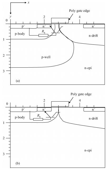
Fig. 1.
Cross section of (a) proposed S-LDMOS (b) and conventional C-LDMOS.
SEMICONDUCTOR DEVICES
Weidong Nie1, 2, , Fayou Yi2 and Zongguang Yu1
Corresponding author: Nie Weidong, Email:youdanwd@163.com
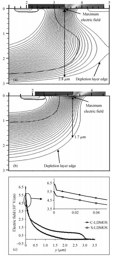
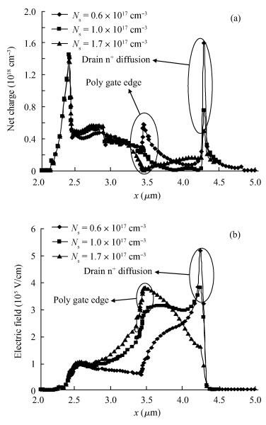
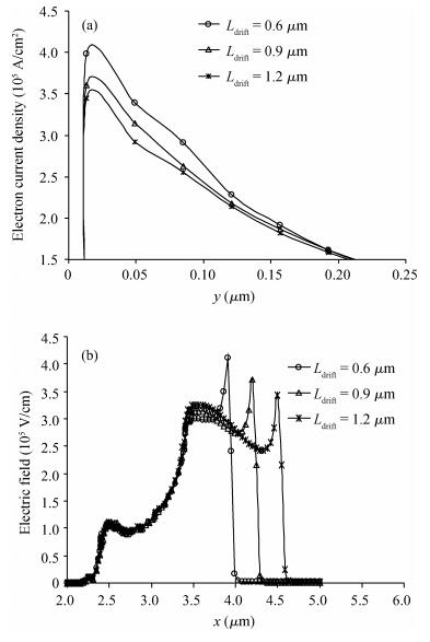
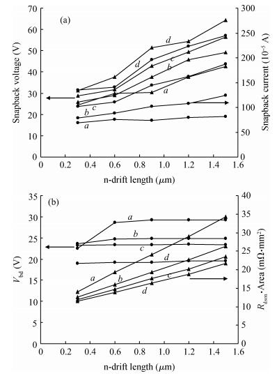
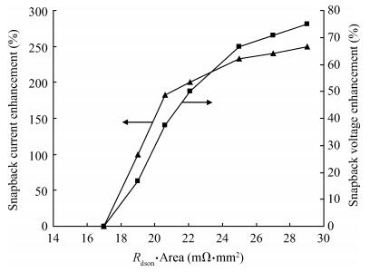
Abstract: For 20 V planar active-gap lateral double-diffused MOSFET (LDMOS), the sectional channel is utilized to decrease the electric field in the n-drift region below the poly gate edge in the off-state, compared with the conventional single channel. Then the n-drift concentration can be increased to decrease the Kirk effect, while keeping off-state breakdown voltage Vbd unchanged. Meanwhile the influence of the n-drift concentration and the n-drift length Ldrift (the drain n+ diffusion to gate spacing) which are related to the Kirk effect is discussed. The trade-offs between Rdson·Area, breakdown voltage Vbd and the electrical safe operating area (e-SOA) performance of LDMOS are considered also. Finally the proposed planar active-gap LDMOS devices with varied values of Ldrift are experimentally demonstrated. The experimental results show that the Kirk effect can be greatly suppressed with slight increase in the Rdson·Area parameter.
Keywords: planar active-gap LDMOS, sectional channel, n-drift length Ldrift, n-drift concentration, Kirk effect, electrical safe operating area
| [1] |
Hower P L, Pendharkar S. Short and long-term safe operating area considerations in LDMOS transistors. IEEE Annual International Reliability Physics Symposium Proceedings, 2005: 545
|
| [2] |
Podgaynaya A, Pogany D, Gornik E, et al. Enhancement of the electrical safe operating area of integrated DMOS transistors with respect to high-energy short duration pulses. IEEE Trans Electron Devices, 2010, 57(11):3044 doi: 10.1109/TED.2010.2069564
|
| [3] |
Shrivastava M, Gossner H, Baghini M S, et al. Part Ⅰ:on the behavior of STI-type DeNMOS device under ESD conditions. IEEE Trans Electron Devices, 2010, 57(9):2235 doi: 10.1109/TED.2010.2055276
|
| [4] |
Steighner J B, Yuan J S. The effect of SOA enhancement on device ruggedness under UIS for the LDMOSFET. IEEE Trans Device Mater Reliab, 2011, 11(2):254 doi: 10.1109/TDMR.2011.2121068
|
| [5] |
Kinoshita K, Kawaguchi Y, Nakagawa A. A new adaptive Resurf concept for 20 V LDMOS without breakdown voltage degradation at high current. Proceedings of International Symposium on Power Semiconductor Devices and ICs, 1998: 65
|
| [6] |
Amerasekera A, Ramaswamy S, Chang M, et al. Modeling MOS snapback and parasitic bipolar action for circuit-level ESD and high current simulations. IEEE Annual International Reliability Physics Symposium Proceedings, 1996: 318
|
| [7] |
Ng K, Lynch W. Analysis of the gate-voltage-dependent series resistance of MOSFETs. IEEE Trans Electron Devices, 1986, 33(7):965 doi: 10.1109/T-ED.1986.22602
|


Article views: 5678 Times PDF downloads: 261 Times Cited by: 0 Times
Received: 24 September 2012 Revised: 12 November 2012 Online: Published: 01 May 2013
| Citation: |
Weidong Nie, Fayou Yi, Zongguang Yu. Kirk effect and suppression for 20 V planar active-gap LDMOS[J]. Journal of Semiconductors, 2013, 34(5): 054003. doi: 10.1088/1674-4926/34/5/054003
****
W D Nie, F Y Yi, Z G Yu. Kirk effect and suppression for 20 V planar active-gap LDMOS[J]. J. Semicond., 2013, 34(5): 054003. doi: 10.1088/1674-4926/34/5/054003.

|
| [1] |
Hower P L, Pendharkar S. Short and long-term safe operating area considerations in LDMOS transistors. IEEE Annual International Reliability Physics Symposium Proceedings, 2005: 545
|
| [2] |
Podgaynaya A, Pogany D, Gornik E, et al. Enhancement of the electrical safe operating area of integrated DMOS transistors with respect to high-energy short duration pulses. IEEE Trans Electron Devices, 2010, 57(11):3044 doi: 10.1109/TED.2010.2069564
|
| [3] |
Shrivastava M, Gossner H, Baghini M S, et al. Part Ⅰ:on the behavior of STI-type DeNMOS device under ESD conditions. IEEE Trans Electron Devices, 2010, 57(9):2235 doi: 10.1109/TED.2010.2055276
|
| [4] |
Steighner J B, Yuan J S. The effect of SOA enhancement on device ruggedness under UIS for the LDMOSFET. IEEE Trans Device Mater Reliab, 2011, 11(2):254 doi: 10.1109/TDMR.2011.2121068
|
| [5] |
Kinoshita K, Kawaguchi Y, Nakagawa A. A new adaptive Resurf concept for 20 V LDMOS without breakdown voltage degradation at high current. Proceedings of International Symposium on Power Semiconductor Devices and ICs, 1998: 65
|
| [6] |
Amerasekera A, Ramaswamy S, Chang M, et al. Modeling MOS snapback and parasitic bipolar action for circuit-level ESD and high current simulations. IEEE Annual International Reliability Physics Symposium Proceedings, 1996: 318
|
| [7] |
Ng K, Lynch W. Analysis of the gate-voltage-dependent series resistance of MOSFETs. IEEE Trans Electron Devices, 1986, 33(7):965 doi: 10.1109/T-ED.1986.22602
|

 WeChat ID
Journal of Semiconductors © 2017 All Rights Reserved 京ICP备05085259号-2

 DownLoad:

