


Fig. 1.
Schematic of the fabrication process for ZnO nanowires on FTO substrate.
SEMICONDUCTOR DEVICES
Zhitao Han1, 2, Sisi Li2, Junjun Li2, Jinkui Chu1 and Yong Chen2,
Corresponding author: Chen Yong, Email:yong.chen@ens.fr
Abstract: Long and well-aligned ZnO nanowires were hydrothermally synthesized on FTO glass based on a ZnO seed layer which was prepared by spin-coating and annealing techniques. The effect of the growth solution refreshment on the morphology of ZnO nanowires was investigated and the possible mechanism was discussed. After refreshing the growth solution for 5 cycles, ZnO nanowires of 120 nm in diameter and 20 μm in length were obtained. The prepared ZnO nanowires were used as photoelectrodes in dye-sensitized solar cells (DSSCs), showing excellent photovoltaic performance. With the increase of growth cycles of ZnO nanowires, the photocurrent of DSSCs increased obviously due to the increased dye loading on the surface of ZnO nanowires. The results indicated that the long and well-aligned ZnO nanowires are promising for DSSCs application.
Keywords: zinc oxide, nanowires, hydrothermal synthesis, dye-sensitized solar cells
| [1] |
Huang M H, Mao S, Feick H, et al. Room-temperature ultraviolet nanowire nanolasers. Science, 2001, 292:1897 doi: 10.1126/science.1060367
|
| [2] |
Ye Z Z, Huang J Y, Xu W Z, et al. Catalyst-free MOCVD growth of aligned ZnO nanotip arrays on silicon substrate with controlled tip shape. Solid-State Commun, 2007, 141(8):464 doi: 10.1016/j.ssc.2006.11.038
|
| [3] |
Zhu Y W, Zhang H Z, Sun X C, et al. Efficient field emission from ZnO nanoneedle arrays. Appl Phys Lett, 2003, 83(11):144
|
| [4] |
Wang X D, Summers C J, Wang Z L. Large-scale hexagonal-patterned growth of aligned ZnO nanorods for nano-optoelectronics and nanosensor arrays. Nano Lett, 2004, 4(3):423 doi: 10.1021/nl035102c
|
| [5] |
Law M, Greene L E, Johnson J C, et al. Nanowire dye-sensitized solar cells. Nat Mater, 2005, 4(6):455 doi: 10.1038/nmat1387
|
| [6] |
Zhang Yongai, Wu Chaoxin, Zheng Yong, et al. Synthesis and efficient field emission characteristics of patterned ZnO nanowires. Journal of Semiconductors, 2012, 33(2):023001 doi: 10.1088/1674-4926/33/2/023001
|
| [7] |
Geng C, Jiang Y, Yao Y, et al. Well-aligned ZnO nanowire arrays fabricated on silicon substrates. Adv Funct Mater, 2004, 14(6):589 doi: 10.1002/(ISSN)1616-3028
|
| [8] |
Jeong M C, Oh B Y, Lee W, et al. Optoelectronic properties of three-dimensional ZnO hybrid structure. Appl Phys Lett, 2005, 86:103105 doi: 10.1063/1.1872209
|
| [9] |
Kar J P, Choi J H, Das S N, et al. Fabrication and characterization of vertically aligned long ZnO nanorods on transparent substrate. J Nanosci Nanotechnol, 2011, 11(3):2185 doi: 10.1166/jnn.2011.3538
|
| [10] |
Sun Y, Fuge G M, Ashfold M N R. Growth of aligned ZnO nanorod arrays by catalyst-free pulsed laser deposition methods. Chem Phys Lett, 2004, 396(1-3):21 doi: 10.1016/j.cplett.2004.07.110
|
| [11] |
Gao X, Li X, Yu W. Flowerlike ZnO nanostructures via hexamethylenetetramine-assisted thermolysis of zinc-ethylenediamine complex. J Phys Chem B, 2005, 109(3):1155 doi: 10.1021/jp046267s
|
| [12] |
Shi Liwei, Li Yuguo, Wang Qiang, et al. Synthesis of one-dimensional ZnO nanorods by oxidating zinc films deposited with magnetron sputtering. Chinese Journal of Semiconductors, 2004, 25(10):1211 http://www.oalib.com/paper/1518492
|
| [13] |
Kim A R, Lee J Y, Jang B R, et al. Effect of buffer layer thickness on the growth properties of hydrothermally grown ZnO nanorods. J Nanosci Nanotechnol, 2011, 11(2):1409 doi: 10.1166/jnn.2011.3395
|
| [14] |
Greene L E, Law M, Dawud H T, et al. General route to vertical ZnO nanowire arrays using textured ZnO seeds. Nano Lett, 2005, 5(7):1231 doi: 10.1021/nl050788p
|
| [15] |
Xu C K, Shin P, Cao L L, et al. Preferential growth of long ZnO nanowire array and its application in dye-sensitized solar cells. J Phys Chem C, 2010, 114(1):125 doi: 10.1021/jp9085415
|
| [16] |
Xu S, Lao C, Weintraub B, et al. Density-controlled growth of aligned ZnO nanowire arrays by seedless chemical approach on smooth surfaces. J Mater Res, 2008, 23(8):2072 doi: 10.1557/JMR.2008.0274
|
| [17] |
Kartawidjaja F C, Lim Z Y, Ng S L G, et al. Morphology, optical, and magnetic properties of Zn1-xCoxO nanorods grown via a wet chemical route. J Am Ceram Soc, 2010, 93(11):3798 doi: 10.1111/jace.2010.93.issue-11
|
| [18] |
Strom J G, Jun H W. Kinetics of hydrolysis of methenamine. J Pharm Sci, 1980, 69(11):1261 doi: 10.1002/jps.2600691107
|
| [19] |
Govender K, Boyle D S, Kenway P B, et al. Understanding the factors that govern the deposition and morphology of thin films of ZnO from aqueous solution. J Mater Chem, 2004, 14:2575 doi: 10.1039/B404784B
|
| [20] |
Greene L E, Yuhas B D, Law M, et al. Solution-grown zinc oxide nanowires. Inorg Chem, 2006, 45(19):7535 doi: 10.1021/ic0601900
|
| [21] |
Yamabi S, Imai H. Growth conditions for wurtzite zinc oxide films in aqueous solutions. J Mater Chem, 2002, 12:3773 doi: 10.1039/b205384e
|
| [22] |
Tian J H, Hu J, Li S S, et al. Improved seedless hydrothermal synthesis of dense and ultralong ZnO nanowires. Nanotechnology, 2011, 22:245601 doi: 10.1088/0957-4484/22/24/245601
|
| [23] |
Kim K S, Jeong H, Jeong M S, et al. Polymer-templated hydrothermal growth of vertically aligned single-crystal ZnO nanorods and morphological transformations using structural polarity. Adv Funct Mater, 2010, 20(18):3055 doi: 10.1002/adfm.201000613
|
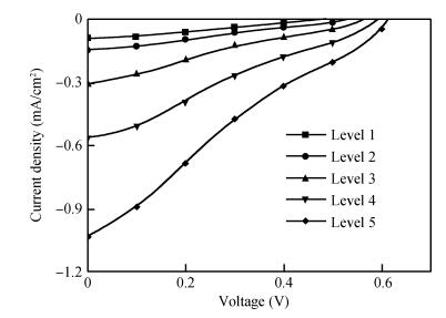
Table 1.

|
| [1] |
Huang M H, Mao S, Feick H, et al. Room-temperature ultraviolet nanowire nanolasers. Science, 2001, 292:1897 doi: 10.1126/science.1060367
|
| [2] |
Ye Z Z, Huang J Y, Xu W Z, et al. Catalyst-free MOCVD growth of aligned ZnO nanotip arrays on silicon substrate with controlled tip shape. Solid-State Commun, 2007, 141(8):464 doi: 10.1016/j.ssc.2006.11.038
|
| [3] |
Zhu Y W, Zhang H Z, Sun X C, et al. Efficient field emission from ZnO nanoneedle arrays. Appl Phys Lett, 2003, 83(11):144
|
| [4] |
Wang X D, Summers C J, Wang Z L. Large-scale hexagonal-patterned growth of aligned ZnO nanorods for nano-optoelectronics and nanosensor arrays. Nano Lett, 2004, 4(3):423 doi: 10.1021/nl035102c
|
| [5] |
Law M, Greene L E, Johnson J C, et al. Nanowire dye-sensitized solar cells. Nat Mater, 2005, 4(6):455 doi: 10.1038/nmat1387
|
| [6] |
Zhang Yongai, Wu Chaoxin, Zheng Yong, et al. Synthesis and efficient field emission characteristics of patterned ZnO nanowires. Journal of Semiconductors, 2012, 33(2):023001 doi: 10.1088/1674-4926/33/2/023001
|
| [7] |
Geng C, Jiang Y, Yao Y, et al. Well-aligned ZnO nanowire arrays fabricated on silicon substrates. Adv Funct Mater, 2004, 14(6):589 doi: 10.1002/(ISSN)1616-3028
|
| [8] |
Jeong M C, Oh B Y, Lee W, et al. Optoelectronic properties of three-dimensional ZnO hybrid structure. Appl Phys Lett, 2005, 86:103105 doi: 10.1063/1.1872209
|
| [9] |
Kar J P, Choi J H, Das S N, et al. Fabrication and characterization of vertically aligned long ZnO nanorods on transparent substrate. J Nanosci Nanotechnol, 2011, 11(3):2185 doi: 10.1166/jnn.2011.3538
|
| [10] |
Sun Y, Fuge G M, Ashfold M N R. Growth of aligned ZnO nanorod arrays by catalyst-free pulsed laser deposition methods. Chem Phys Lett, 2004, 396(1-3):21 doi: 10.1016/j.cplett.2004.07.110
|
| [11] |
Gao X, Li X, Yu W. Flowerlike ZnO nanostructures via hexamethylenetetramine-assisted thermolysis of zinc-ethylenediamine complex. J Phys Chem B, 2005, 109(3):1155 doi: 10.1021/jp046267s
|
| [12] |
Shi Liwei, Li Yuguo, Wang Qiang, et al. Synthesis of one-dimensional ZnO nanorods by oxidating zinc films deposited with magnetron sputtering. Chinese Journal of Semiconductors, 2004, 25(10):1211 http://www.oalib.com/paper/1518492
|
| [13] |
Kim A R, Lee J Y, Jang B R, et al. Effect of buffer layer thickness on the growth properties of hydrothermally grown ZnO nanorods. J Nanosci Nanotechnol, 2011, 11(2):1409 doi: 10.1166/jnn.2011.3395
|
| [14] |
Greene L E, Law M, Dawud H T, et al. General route to vertical ZnO nanowire arrays using textured ZnO seeds. Nano Lett, 2005, 5(7):1231 doi: 10.1021/nl050788p
|
| [15] |
Xu C K, Shin P, Cao L L, et al. Preferential growth of long ZnO nanowire array and its application in dye-sensitized solar cells. J Phys Chem C, 2010, 114(1):125 doi: 10.1021/jp9085415
|
| [16] |
Xu S, Lao C, Weintraub B, et al. Density-controlled growth of aligned ZnO nanowire arrays by seedless chemical approach on smooth surfaces. J Mater Res, 2008, 23(8):2072 doi: 10.1557/JMR.2008.0274
|
| [17] |
Kartawidjaja F C, Lim Z Y, Ng S L G, et al. Morphology, optical, and magnetic properties of Zn1-xCoxO nanorods grown via a wet chemical route. J Am Ceram Soc, 2010, 93(11):3798 doi: 10.1111/jace.2010.93.issue-11
|
| [18] |
Strom J G, Jun H W. Kinetics of hydrolysis of methenamine. J Pharm Sci, 1980, 69(11):1261 doi: 10.1002/jps.2600691107
|
| [19] |
Govender K, Boyle D S, Kenway P B, et al. Understanding the factors that govern the deposition and morphology of thin films of ZnO from aqueous solution. J Mater Chem, 2004, 14:2575 doi: 10.1039/B404784B
|
| [20] |
Greene L E, Yuhas B D, Law M, et al. Solution-grown zinc oxide nanowires. Inorg Chem, 2006, 45(19):7535 doi: 10.1021/ic0601900
|
| [21] |
Yamabi S, Imai H. Growth conditions for wurtzite zinc oxide films in aqueous solutions. J Mater Chem, 2002, 12:3773 doi: 10.1039/b205384e
|
| [22] |
Tian J H, Hu J, Li S S, et al. Improved seedless hydrothermal synthesis of dense and ultralong ZnO nanowires. Nanotechnology, 2011, 22:245601 doi: 10.1088/0957-4484/22/24/245601
|
| [23] |
Kim K S, Jeong H, Jeong M S, et al. Polymer-templated hydrothermal growth of vertically aligned single-crystal ZnO nanorods and morphological transformations using structural polarity. Adv Funct Mater, 2010, 20(18):3055 doi: 10.1002/adfm.201000613
|


Article views: 2936 Times PDF downloads: 26 Times Cited by: 0 Times
Received: 03 December 2012 Revised: 09 January 2013 Online: Published: 01 July 2013
| Citation: |
Zhitao Han, Sisi Li, Junjun Li, Jinkui Chu, Yong Chen. Facile synthesis of ZnO nanowires on FTO glass for dye-sensitized solar cells[J]. Journal of Semiconductors, 2013, 34(7): 074002. doi: 10.1088/1674-4926/34/7/074002
****
Z T Han, S S Li, J J Li, J K Chu, Y Chen. Facile synthesis of ZnO nanowires on FTO glass for dye-sensitized solar cells[J]. J. Semicond., 2013, 34(7): 074002. doi: 10.1088/1674-4926/34/7/074002.

|
| [1] |
Huang M H, Mao S, Feick H, et al. Room-temperature ultraviolet nanowire nanolasers. Science, 2001, 292:1897 doi: 10.1126/science.1060367
|
| [2] |
Ye Z Z, Huang J Y, Xu W Z, et al. Catalyst-free MOCVD growth of aligned ZnO nanotip arrays on silicon substrate with controlled tip shape. Solid-State Commun, 2007, 141(8):464 doi: 10.1016/j.ssc.2006.11.038
|
| [3] |
Zhu Y W, Zhang H Z, Sun X C, et al. Efficient field emission from ZnO nanoneedle arrays. Appl Phys Lett, 2003, 83(11):144
|
| [4] |
Wang X D, Summers C J, Wang Z L. Large-scale hexagonal-patterned growth of aligned ZnO nanorods for nano-optoelectronics and nanosensor arrays. Nano Lett, 2004, 4(3):423 doi: 10.1021/nl035102c
|
| [5] |
Law M, Greene L E, Johnson J C, et al. Nanowire dye-sensitized solar cells. Nat Mater, 2005, 4(6):455 doi: 10.1038/nmat1387
|
| [6] |
Zhang Yongai, Wu Chaoxin, Zheng Yong, et al. Synthesis and efficient field emission characteristics of patterned ZnO nanowires. Journal of Semiconductors, 2012, 33(2):023001 doi: 10.1088/1674-4926/33/2/023001
|
| [7] |
Geng C, Jiang Y, Yao Y, et al. Well-aligned ZnO nanowire arrays fabricated on silicon substrates. Adv Funct Mater, 2004, 14(6):589 doi: 10.1002/(ISSN)1616-3028
|
| [8] |
Jeong M C, Oh B Y, Lee W, et al. Optoelectronic properties of three-dimensional ZnO hybrid structure. Appl Phys Lett, 2005, 86:103105 doi: 10.1063/1.1872209
|
| [9] |
Kar J P, Choi J H, Das S N, et al. Fabrication and characterization of vertically aligned long ZnO nanorods on transparent substrate. J Nanosci Nanotechnol, 2011, 11(3):2185 doi: 10.1166/jnn.2011.3538
|
| [10] |
Sun Y, Fuge G M, Ashfold M N R. Growth of aligned ZnO nanorod arrays by catalyst-free pulsed laser deposition methods. Chem Phys Lett, 2004, 396(1-3):21 doi: 10.1016/j.cplett.2004.07.110
|
| [11] |
Gao X, Li X, Yu W. Flowerlike ZnO nanostructures via hexamethylenetetramine-assisted thermolysis of zinc-ethylenediamine complex. J Phys Chem B, 2005, 109(3):1155 doi: 10.1021/jp046267s
|
| [12] |
Shi Liwei, Li Yuguo, Wang Qiang, et al. Synthesis of one-dimensional ZnO nanorods by oxidating zinc films deposited with magnetron sputtering. Chinese Journal of Semiconductors, 2004, 25(10):1211 http://www.oalib.com/paper/1518492
|
| [13] |
Kim A R, Lee J Y, Jang B R, et al. Effect of buffer layer thickness on the growth properties of hydrothermally grown ZnO nanorods. J Nanosci Nanotechnol, 2011, 11(2):1409 doi: 10.1166/jnn.2011.3395
|
| [14] |
Greene L E, Law M, Dawud H T, et al. General route to vertical ZnO nanowire arrays using textured ZnO seeds. Nano Lett, 2005, 5(7):1231 doi: 10.1021/nl050788p
|
| [15] |
Xu C K, Shin P, Cao L L, et al. Preferential growth of long ZnO nanowire array and its application in dye-sensitized solar cells. J Phys Chem C, 2010, 114(1):125 doi: 10.1021/jp9085415
|
| [16] |
Xu S, Lao C, Weintraub B, et al. Density-controlled growth of aligned ZnO nanowire arrays by seedless chemical approach on smooth surfaces. J Mater Res, 2008, 23(8):2072 doi: 10.1557/JMR.2008.0274
|
| [17] |
Kartawidjaja F C, Lim Z Y, Ng S L G, et al. Morphology, optical, and magnetic properties of Zn1-xCoxO nanorods grown via a wet chemical route. J Am Ceram Soc, 2010, 93(11):3798 doi: 10.1111/jace.2010.93.issue-11
|
| [18] |
Strom J G, Jun H W. Kinetics of hydrolysis of methenamine. J Pharm Sci, 1980, 69(11):1261 doi: 10.1002/jps.2600691107
|
| [19] |
Govender K, Boyle D S, Kenway P B, et al. Understanding the factors that govern the deposition and morphology of thin films of ZnO from aqueous solution. J Mater Chem, 2004, 14:2575 doi: 10.1039/B404784B
|
| [20] |
Greene L E, Yuhas B D, Law M, et al. Solution-grown zinc oxide nanowires. Inorg Chem, 2006, 45(19):7535 doi: 10.1021/ic0601900
|
| [21] |
Yamabi S, Imai H. Growth conditions for wurtzite zinc oxide films in aqueous solutions. J Mater Chem, 2002, 12:3773 doi: 10.1039/b205384e
|
| [22] |
Tian J H, Hu J, Li S S, et al. Improved seedless hydrothermal synthesis of dense and ultralong ZnO nanowires. Nanotechnology, 2011, 22:245601 doi: 10.1088/0957-4484/22/24/245601
|
| [23] |
Kim K S, Jeong H, Jeong M S, et al. Polymer-templated hydrothermal growth of vertically aligned single-crystal ZnO nanorods and morphological transformations using structural polarity. Adv Funct Mater, 2010, 20(18):3055 doi: 10.1002/adfm.201000613
|

 WeChat ID
Journal of Semiconductors © 2017 All Rights Reserved 京ICP备05085259号-2

 DownLoad:

