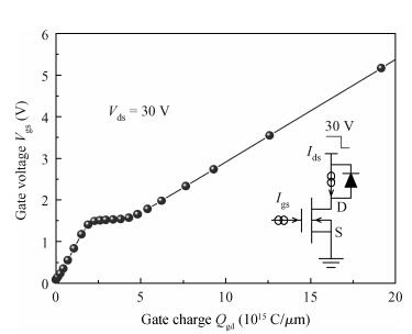
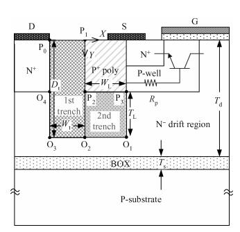
| [1] |
Luo X, Zhang B, Li Z, et al. A novel 700-V SOI LDMOS with double-sided trench. IEEE Electron Device Lett, 2007, 28:422 doi: 10.1109/LED.2007.894648 |
| [2] |
Luo X R, Yao G L, Chen X, et al. Ultra-low on-resistance high voltage (> 600 V) SOI MOSFET with a reduced cell pitch. Chin Phys B, 2011, 20(2):028501 doi: 10.1088/1674-1056/20/2/028501 |
| [3] |
Ren M, Li Z H, Liu X L, et al. A novel planar vertical double-diffused metal-oxide-semiconductor field-effect transistor with inhomogeneous floating islands. Chin Phys B, 2011, 20(12):128501 doi: 10.1088/1674-1056/20/12/128501 |
| [4] |
Wang C L, Sun J. An oxide filled extended trench gate super junction MOSFET structure. Chin Phys B, 2009, 18(3):1231 doi: 10.1088/1674-1056/18/3/065 |
| [5] |
Luo Xiaorong, Zhang Wei, Gu Jingjing, et al. A new double gate SOI LDMOS with a step doping profile in the drift region. Journal of Semiconductors, 2009, 30:084006 doi: 10.1088/1674-4926/30/8/084006 |
| [6] |
Radhakrishna U, DasGupta A, DasGupta N, et al. Modeling of SOI-LDMOS transistor including impact ionization, snapback, and self-heating. IEEE Trans Electron Devices, 2011, 58:4035 doi: 10.1109/TED.2011.2165724 |
| [7] |
Son W S, Sohn Y H, Choi S Y. SOI RESURF LDMOS transistor using trench filled with oxide. Electron Lett, 2003, 39:1760 doi: 10.1049/el:20031115 |
| [8] |
Leung Y K, Paul A K, Goodson K E, et al. Heating mechanisms of LDMOS and LIGBT in ultrathin SOI. IEEE Electron Device Lett, 1997, 18(9):414 doi: 10.1109/55.622514 |
| [9] |
|
| [10] |
Murthy B R, Mukherjee-Roy M, Krishnamoorthy A, et al. Reactive ion etching and characterization of p-silk ultra low- k film. IEEE Trans Semicond Manuf, 2005, 18:174 doi: 10.1109/TSM.2004.840537 |
| [11] |
Luo X, Udrea F, Wang Y, et al. Partial SOI power LDMOS with a variable low- k dielectric buried layer and a buried P layer. IEEE Electron Device Lett, 2010, 31(6):594 doi: 10.1109/LED.2010.2046616 |
| [12] |
Lubguban J J, Seitob A, Kurata Y, et al. Stability of the dielectric properties of PECVD deposited carbon-doped SiOF films. Thin Solid Films, 1999, 337(1/2):67
|
| [13] |
Yoneda K, Kato M, Nakao S, et al. Robust low- k diffusion barrier (k=3.5) for 45-nm node low- k (k=2.3)/Cu integration. Proc Interconnect Technology Conference, 2006:184 doi: 10.1007/978-0-387-95868-2_21/fulltext.html |
| [14] |
Théolier L, Mahfoz-Kotb H, Isoird K, et al. A new junction termination using a deep trench filled with benzocyclobutene. IEEE Electron Device Lett, 2009, 30(6):687 doi: 10.1109/LED.2009.2020348 |
| [15] |
Wang Y, Jiao W L, Hu H F, et al. A gate enhanced power U-shaped MOSFET integrated with a Schottky rectifier. Chin Phys B, 2012, 21(5):056104 doi: 10.1088/1674-1056/21/5/056104 |
| [16] |
Li Xiaorong, Zhang Bo, Li Zhaoji, et al. A novel SOI high voltage device structure with a partial locating charge trench. Chinese Journal of Electronics, 2006, 27(5):881 doi: 10.1007/s10825-017-0994-7 |
| [17] |
Li W Y, Ru G P, Jiang Y L, et al. Trapezoid mesa trench metal-oxide-semiconductor barrier Schottky rectifier:an improved Schottky rectifier with better reverse characteristics. Chin Phys B, 2011, 20(8):087304 doi: 10.1088/1674-1056/20/8/087304 |
| [18] |
Moens P, Boschd G V. Characterization of total safe operating area of lateral DMOS transistors. IEEE Trans Device Mater Reliab, 2006, 6:349 doi: 10.1109/TDMR.2006.882212 |
| [19] |
Khemka V, Parthasarathy V, Zhu R, et al. Experimental and theoretical analysis of energy capability of RESURF LDMOSFETs and its correlation with static electrical safe operating area (SOA). IEEE Trans Electron Devices, 2002, 49:1049 doi: 10.1109/TED.2002.1003740 |
| [20] |
Ren M, Li Z H, Deng G M, et al. A novel superjunction MOSFET with improved ruggedness under unclamped inductive switching. Chin Phys B, 2012, 21(4):048502 doi: 10.1088/1674-1056/21/4/048502 |
| [21] |
|
| [22] |
Yin Shan, Qiao Ming, Zhang Yongman, et al. Design of 700 V triple RESURF nLDMOS with low on-resistance. Journal of Semiconductors, 2011, 32:114002 doi: 10.1088/1674-4926/32/11/114002 |
| [23] |
Li Z J, Zhang B, Luo X R, et al. The rule of field enhancement for buried dielectric layer of SQl high voltage devices. Proc ICCCAS, 2007:1302
|
| [24] |
Zhang B, Li Z, Hu S, et al. Field enhancement for dielectric layer of high-voltage devices on silicon on insulator. IEEE Trans Electron Devices, 2009, 56:2327 doi: 10.1109/TED.2009.2028405 |
| [25] |
Wu L J, Hu S D, Luo X R, et al. Partial-SOI high voltage P-channel LDMOS with interface accumulation holes. Chin Phys B, 2011, 20(10):107101 doi: 10.1088/1674-1056/20/10/107101 |
| [26] |
Tang Z, Ye P D, Lee D, et al. Electrical measurements of voltage stressed Al 2O 3/GaAs MOSFET. Microelectron Reliab, 2007, 47(12):2082 doi: 10.1016/j.microrel.2007.02.012 |
| [27] |
Moens P, Van den bosch G. Characterization of total safe operating area of lateral DMOS transistors. IEEE Trans Device Mater Reliab, 2006, 6(3):349 doi: 10.1109/TDMR.2006.882212 |
| [28] |
Pendharkar S, Higgins R, Debolske T, et al. Optimization of low voltage n-channel LDMOS devices to achieve required electrical and lifetime SOA. Proceedings of the 14th International Symposium on Power Semiconductor Devices and ICs, 2002:261 doi: 10.1007/978-3-319-08994-2_11 |
| [29] |
Moens P, Van den Bosch G, De Keukeleire C, et al. Hot hole degradation effects in lateral nDMOS transistors. IEEE Trans Electron Devices, 2004, 51(10):1704 doi: 10.1109/TED.2004.834913 |
| [30] |
Wang P F, Ding S J, Zhang W, et al. CVD technologies used in preparation of low materials for ULSI. Microfabrication Technol, 2001, 1:30
|
| [31] |
|
| [32] |
|
| [33] |
Steighner J B, Yuan J S. The effect of SOA enhancement on device ruggedness under UIS for the LDMOSFET. IEEE Trans Device Mater Reliab, 2011, 11(2):254 doi: 10.1109/TDMR.2011.2121068 |
| [34] |
Zhu R, Khemka V, Bose A, et al. Substrate majority carrier-induced NLDMOSFET failure and its prevention in advanced smart power IC technologies. IEEE Trans Device Mater Reliab, 2006, 6(3):386 doi: 10.1109/TDMR.2006.882198 |
| [35] |
Lee C P, Chati F H E, Ma W, et al. The safe operating area of GaAs-based heterojunction bipolar transistors. IEEE Trans Electron Devices, 2006, 53(11):2681 doi: 10.1109/TED.2006.884075 |
| [36] |
In't Zandt M A A, Hijzen E A, Hueting R J E, et al. Record-low 4 mΩ·mm2 specific on-resistance for 20 V trench MOSFETs. Proc ISPSD, 2003:32
|
| [37] |
Jiang Q, Wang M, Chen X, et al. A high-speed deep-trench MOSFET with a self-biased split gate. IEEE Trans Electron Devices. 2010, 57:1972 doi: 10.1109/TED.2010.2051247 |
| [38] |
Rutter P, Peake S T. Low voltage trench MOS combining low specific R DS(on) and Q G FOM. Proc ISPSD, 2010:325 doi: 10.1007/978-94-007-1926-2_17 |


 DownLoad: