


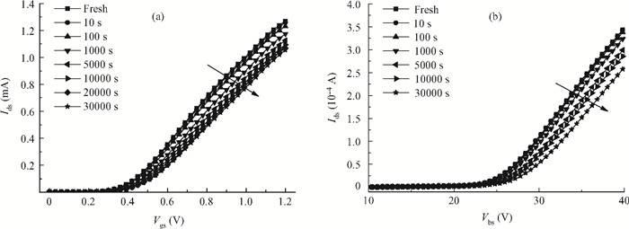
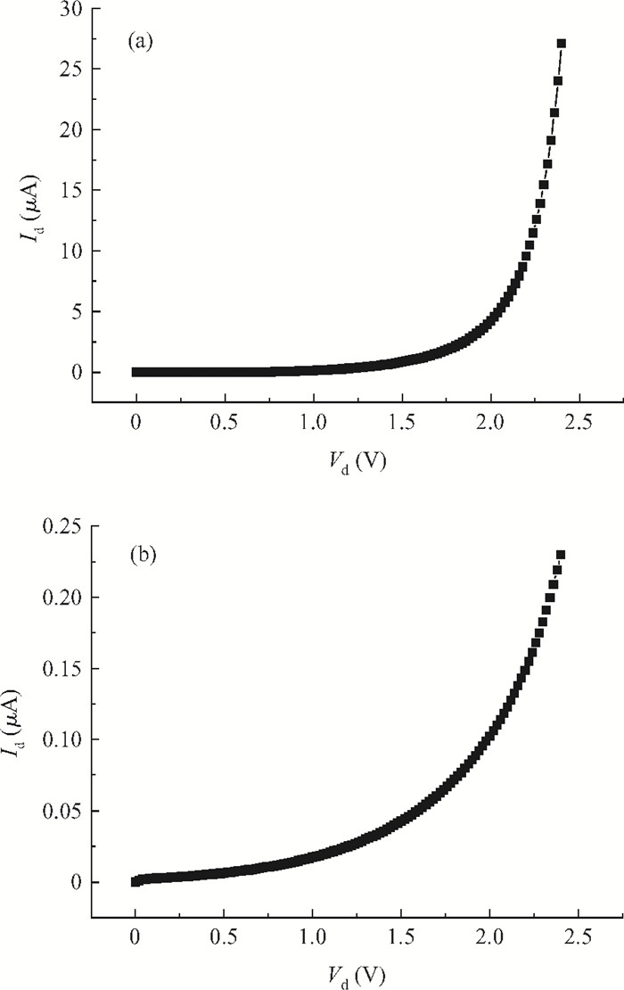
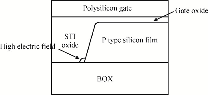
Fig. 1.
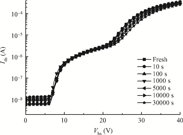
Sub-threshold curves changing with stress for (a) front gate and (b) back gate transistor.
SEMICONDUCTOR DEVICES
Qiwen Zheng1, 2, 3, Xuefeng Yu1, 2, , Jiangwei Cui1, 2, Qi Guo1, 2, Zhongchao Cong1, 2, 3, Xingyao Zhang1, 2, 3, Wei Deng1, 2, 3, Xiaofu Zhang1, 2, 3 and Zhengxin Wu1, 2, 3
Corresponding author: Yu Xuefeng, Email:yuxf@ms.xjb.ac.cn
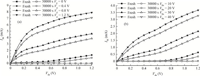
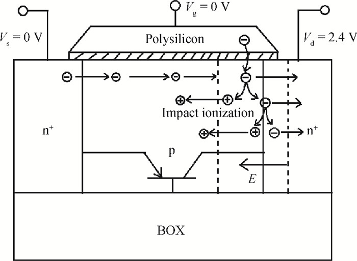
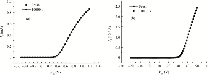
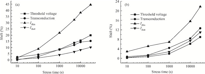
Abstract: The hot-carrier effect characteristic in a deep submicron partially depleted SOI NMOSFET is investigated. Obvious hot-carrier degradation is observed under off-state stress. The hot-carrier damage is supposed to be induced by the parasitic bipolar effects of a float SOI device. The back channel also suffers degradation from the hot carrier in the drain depletion region as well as the front channel. At low gate voltage, there is a hump in the sub-threshold curve of the back gate transistor, and it does not shift in the same way as the main transistor under stress. While under the same condition, there is a more severe hot-carrier effect with a shorter channel transistor. The reasons for those phenomena are discussed in detail.
Keywords: silicon-on-insulator, hot-carrier effect, hump, back gate
| [1] |
Schwank J R, Ferlet-Cavrois V, Shaneyfelt M R. Radiation effects in SOI technologies. IEEE Trans Nucl Sci, 2003, 50(3):522 doi: 10.1109/TNS.2003.812930
|
| [2] |
Cui J W, Yu X F, Ren D Y, et al. Double humps and radiation effects of SOI NMOSFET. Journal of Semiconductors, 2011, 32(6):064006 doi: 10.1088/1674-4926/32/6/064006
|
| [3] |
Liu M X, Han Z S, Bi J S, et al. Effect of total ionizing dose radiation on the 0.25μm RF PDSOI nMOSFETs with thin gate oxide. Journal of Semiconductors, 2009, 30(1):014004 doi: 10.1088/1674-4926/30/1/014004
|
| [4] |
Cristoloveanu S, Li S. Electrical characterization of silicon-on-insulator materials and devices. Boston:Kluwer Academic Publishers, 1995 doi: 10.1007%2F978-1-4615-2245-4
|
| [5] |
Colinge J P. Hot-electron effects in silicon-on-insulator n-channel MOSFET's. IEEE Trans Electron Devices, 1987, ED-34:2173 http://ieeexplore.ieee.org/document/1486924/
|
| [6] |
Chen J J, Chen S M, Liang B, et al. Hot carrier effects of SOI NMOS. Journal of Semiconductors, 2010, 31(7):074006 doi: 10.1088/1674-4926/31/7/074006
|
| [7] |
Shing H R, Emmanuel R, Jean L P. Hot-carrier effects and lifetime prediction in off-state operation of deep submicron SOI N-MOSFET's. IEEE Trans Electron Devices, 1998, 45(5):1140 doi: 10.1109/16.669572
|
| [8] |
Rafi J M, Simoen E, Mercha A, et al. Impact of hot-carrier stress on gate-induced floating body effects and drain current transients of thin gate oxide partially depleted SOI nMOSFETs. Microelectron Reliab, 2005, (49):1536 http://adsabs.harvard.edu/abs/2005SSEle..49.1536R
|
| [9] |
He J, Zhang X, Huang R, et al. A refined forward gated-diode method for separating front channel hot-carrier-stress induced front and back gate interface and oxide traps in SOI NMOSFETs. Semicond Sci Technol, 2002, 17:487 doi: 10.1088/0268-1242/17/5/314
|
| [10] |
Thierry O, Sorin C, Girard B. Hot-carrier-induced degradation of the back interface in short-channel silicon-on-insulator MOSFET's. IEEE Electron Device Lett, 1991, 12(6):290 doi: 10.1109/55.82064
|
| [11] |
Eiji T, Cary Y Y, Akemi M H. Hot carrier effects in MOS device. Academic Press Inc, 1995 http://www.sciencedirect.com/science/article/pii/0026271493900819
|
| [12] |
Mercha A, Rafí J M, Simoen E. Linear kink effect induced by electron valence band tunneling in ultrathin gate oxide bulk and SOI MOSFETs. IEEE Trans Electron Devices, 2003, 50(7):1657 http://ieeexplore.ieee.org/document/1217253/
|
| [13] |
Cristoloveanu S, Gulwadi S M, Ioannou D E. Hot-electron-induced degradation of front and back channels in partially and fully depleted SIMOX MOSFET's. IEEE Electron Device Lett, 1992, 13(12):603 doi: 10.1109/55.192858
|
| [14] |
Jian C, Tung Y C, Ping K K, et al. Gate current in off-state MOSFET. IEEE Electron Device Lett, 1989, 10(5):203 doi: 10.1109/55.31721
|
| [15] |
Jian C, Fariborz A, Ping K, et al. The enhancement of gate-induced-drain-leakage (GIDL) current in short-channel SOI MOSFET and its application in measuring lateral bipolar current gain β. IEEE Electron Device Lett, 1992, 13(11):572 doi: 10.1109/55.192844
|
| [16] |
Jin Y C, Jerry G F. Analysis and control of floating-body bipolar effects in fully depleted submicrometer SOI MOSFET's. IEEE Electron Device, 1991, 38(6):1384 doi: 10.1109/16.81630
|
| [17] |
Jian C, Fariborz A, Hsing J W, et al. An accurate model of thin film SOI MOSFET breakdown voltage. Technical Digest of International Electron Devices Meeting, 1991:671 http://ieeexplore.ieee.org/document/235333/?arnumber=235333
|
| [18] |
Sinha S P, Franklin L D, Dimitris E I. Time dependence power laws of hot carrier degradation in SOI MOSFETS. Proceedings IEEE International SOI Conference, 1996 http://ieeexplore.ieee.org/document/552472/?reload=true&arnumber=552472&count=85&index=8
|
| [19] |
Fenouillet C, Faynot O, Tabone C. Characterization and simulation of STI isolation for 0.1μm partially-depleted SOI devices. IEEE International SOI Conference, 2001:87
|
| [20] |
Ning B, Bi D, Huang H. Bias dependence of TID radiation responses of 0.13μm partially depleted SOI NMOSFETs. Microelectron Reliab, 2013, 53(2):259 doi: 10.1016/j.microrel.2012.08.005
|
| [21] |
Choi J Y, Fossum J G. Analysis and control of floating-body bipolar effects in fully depleted submicrometer SOI MOSFET's. IEEE Trans Electron Devices, 1991, 38(6):1384 doi: 10.1109/16.81630
|


Article views: 3070 Times PDF downloads: 20 Times Cited by: 0 Times
Received: 03 December 2012 Revised: 21 January 2013 Online: Published: 01 July 2013
| Citation: |
Qiwen Zheng, Xuefeng Yu, Jiangwei Cui, Qi Guo, Zhongchao Cong, Xingyao Zhang, Wei Deng, Xiaofu Zhang, Zhengxin Wu. Degradation of the front and back channels in a deep submicron partially depleted SOI NMOSFET under off-state stress[J]. Journal of Semiconductors, 2013, 34(7): 074008. doi: 10.1088/1674-4926/34/7/074008
****
Q W Zheng, X F Yu, J W Cui, Q Guo, Z C Cong, X Y Zhang, W Deng, X F Zhang, Z X Wu. Degradation of the front and back channels in a deep submicron partially depleted SOI NMOSFET under off-state stress[J]. J. Semicond., 2013, 34(7): 074008. doi: 10.1088/1674-4926/34/7/074008.

|
| [1] |
Schwank J R, Ferlet-Cavrois V, Shaneyfelt M R. Radiation effects in SOI technologies. IEEE Trans Nucl Sci, 2003, 50(3):522 doi: 10.1109/TNS.2003.812930
|
| [2] |
Cui J W, Yu X F, Ren D Y, et al. Double humps and radiation effects of SOI NMOSFET. Journal of Semiconductors, 2011, 32(6):064006 doi: 10.1088/1674-4926/32/6/064006
|
| [3] |
Liu M X, Han Z S, Bi J S, et al. Effect of total ionizing dose radiation on the 0.25μm RF PDSOI nMOSFETs with thin gate oxide. Journal of Semiconductors, 2009, 30(1):014004 doi: 10.1088/1674-4926/30/1/014004
|
| [4] |
Cristoloveanu S, Li S. Electrical characterization of silicon-on-insulator materials and devices. Boston:Kluwer Academic Publishers, 1995 doi: 10.1007%2F978-1-4615-2245-4
|
| [5] |
Colinge J P. Hot-electron effects in silicon-on-insulator n-channel MOSFET's. IEEE Trans Electron Devices, 1987, ED-34:2173 http://ieeexplore.ieee.org/document/1486924/
|
| [6] |
Chen J J, Chen S M, Liang B, et al. Hot carrier effects of SOI NMOS. Journal of Semiconductors, 2010, 31(7):074006 doi: 10.1088/1674-4926/31/7/074006
|
| [7] |
Shing H R, Emmanuel R, Jean L P. Hot-carrier effects and lifetime prediction in off-state operation of deep submicron SOI N-MOSFET's. IEEE Trans Electron Devices, 1998, 45(5):1140 doi: 10.1109/16.669572
|
| [8] |
Rafi J M, Simoen E, Mercha A, et al. Impact of hot-carrier stress on gate-induced floating body effects and drain current transients of thin gate oxide partially depleted SOI nMOSFETs. Microelectron Reliab, 2005, (49):1536 http://adsabs.harvard.edu/abs/2005SSEle..49.1536R
|
| [9] |
He J, Zhang X, Huang R, et al. A refined forward gated-diode method for separating front channel hot-carrier-stress induced front and back gate interface and oxide traps in SOI NMOSFETs. Semicond Sci Technol, 2002, 17:487 doi: 10.1088/0268-1242/17/5/314
|
| [10] |
Thierry O, Sorin C, Girard B. Hot-carrier-induced degradation of the back interface in short-channel silicon-on-insulator MOSFET's. IEEE Electron Device Lett, 1991, 12(6):290 doi: 10.1109/55.82064
|
| [11] |
Eiji T, Cary Y Y, Akemi M H. Hot carrier effects in MOS device. Academic Press Inc, 1995 http://www.sciencedirect.com/science/article/pii/0026271493900819
|
| [12] |
Mercha A, Rafí J M, Simoen E. Linear kink effect induced by electron valence band tunneling in ultrathin gate oxide bulk and SOI MOSFETs. IEEE Trans Electron Devices, 2003, 50(7):1657 http://ieeexplore.ieee.org/document/1217253/
|
| [13] |
Cristoloveanu S, Gulwadi S M, Ioannou D E. Hot-electron-induced degradation of front and back channels in partially and fully depleted SIMOX MOSFET's. IEEE Electron Device Lett, 1992, 13(12):603 doi: 10.1109/55.192858
|
| [14] |
Jian C, Tung Y C, Ping K K, et al. Gate current in off-state MOSFET. IEEE Electron Device Lett, 1989, 10(5):203 doi: 10.1109/55.31721
|
| [15] |
Jian C, Fariborz A, Ping K, et al. The enhancement of gate-induced-drain-leakage (GIDL) current in short-channel SOI MOSFET and its application in measuring lateral bipolar current gain β. IEEE Electron Device Lett, 1992, 13(11):572 doi: 10.1109/55.192844
|
| [16] |
Jin Y C, Jerry G F. Analysis and control of floating-body bipolar effects in fully depleted submicrometer SOI MOSFET's. IEEE Electron Device, 1991, 38(6):1384 doi: 10.1109/16.81630
|
| [17] |
Jian C, Fariborz A, Hsing J W, et al. An accurate model of thin film SOI MOSFET breakdown voltage. Technical Digest of International Electron Devices Meeting, 1991:671 http://ieeexplore.ieee.org/document/235333/?arnumber=235333
|
| [18] |
Sinha S P, Franklin L D, Dimitris E I. Time dependence power laws of hot carrier degradation in SOI MOSFETS. Proceedings IEEE International SOI Conference, 1996 http://ieeexplore.ieee.org/document/552472/?reload=true&arnumber=552472&count=85&index=8
|
| [19] |
Fenouillet C, Faynot O, Tabone C. Characterization and simulation of STI isolation for 0.1μm partially-depleted SOI devices. IEEE International SOI Conference, 2001:87
|
| [20] |
Ning B, Bi D, Huang H. Bias dependence of TID radiation responses of 0.13μm partially depleted SOI NMOSFETs. Microelectron Reliab, 2013, 53(2):259 doi: 10.1016/j.microrel.2012.08.005
|
| [21] |
Choi J Y, Fossum J G. Analysis and control of floating-body bipolar effects in fully depleted submicrometer SOI MOSFET's. IEEE Trans Electron Devices, 1991, 38(6):1384 doi: 10.1109/16.81630
|

 WeChat ID
Journal of Semiconductors © 2017 All Rights Reserved 京ICP备05085259号-2

 DownLoad:

