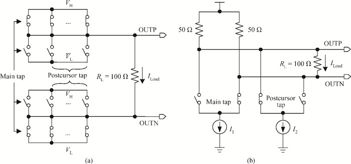
Fig. 1.
Equivalent circuit of the 2-tap (a) VM and (b) CM pre-emphasis output driver.
SEMICONDUCTOR INTEGRATED CIRCUITS
Junsheng Lü, Hao Ju, Mao Ye, Feng Zhang, Jianzhong Zhao and Yumei Zhou
Corresponding author: Lü Junsheng, Email:junsheng.lv@gmail.com
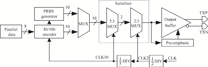
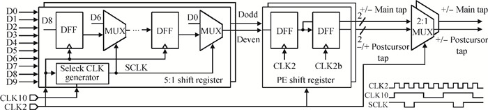
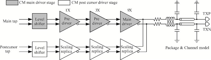
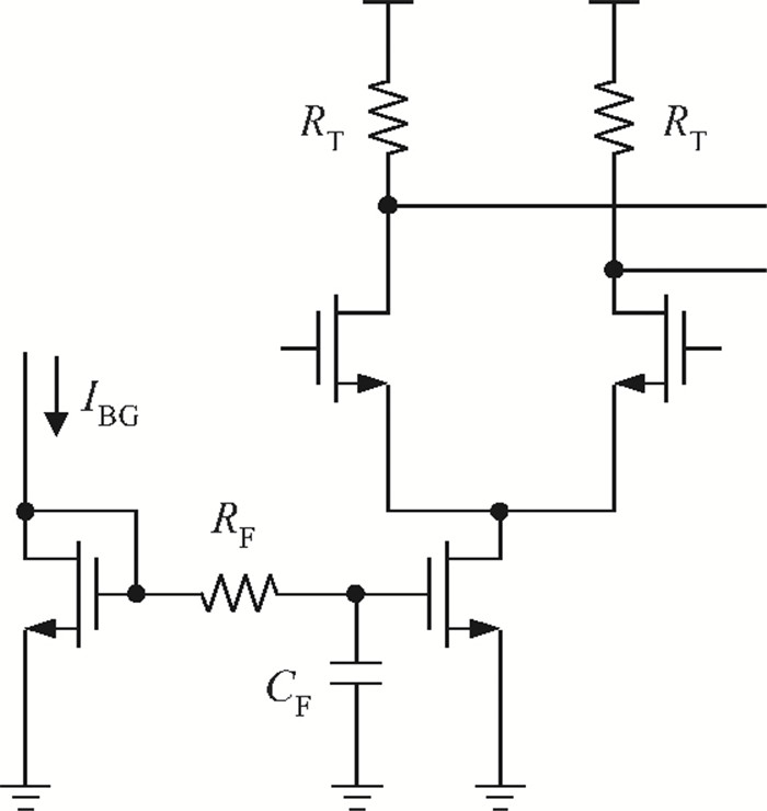
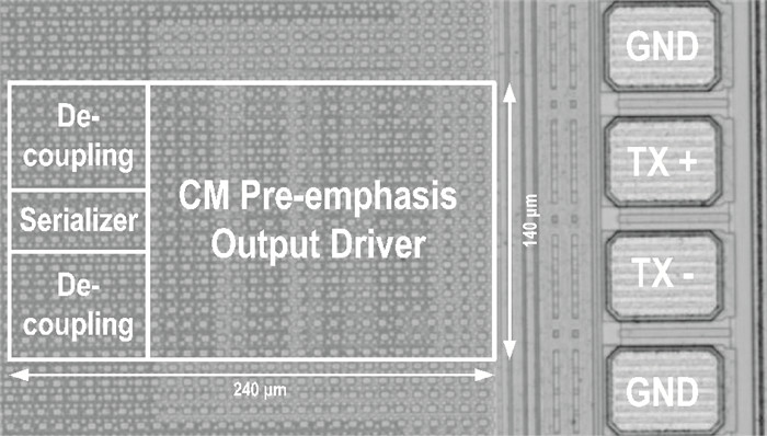
Abstract: A multi-standard compatible transmitter with pre-emphasis for high speed serial links is presented. Based on the comparison between voltage mode (VM) and current mode (CM) output driver architectures, a low power CM output driver with reverse scaling and bias current filtering technique is proposed. A 2-tap pre-emphasis filter is used to reduce the intersymbol interference caused by the low-pass channel, and a high speed, low power combined serializer is implemented to convert 10 bit parallel data into a serial data stream. The whole transmitter is fabricated in 65 nm 1.2 V/2.5 V CMOS technology. It provides an eye height greater than 800 mV for data rates of both 2.5 Gb/s and 5 Gb/s. The output root mean square jitter of the transmitter at 5 Gb/s is only 9.94 ps without pre-emphasis. The transmitter consumes 41.2 mA at 5 Gb/s and occupies only 240×140 μm2.
Keywords: high speed serial links, low power, transmitter, pre-emphasis, reverse scaling, bias current filtering
| [1] |
PCI Express Base Specification Rev 2. 1. PCI-SIG, 2009
|
| [2] |
Fukuda K, Yamashita H, Ono G, et al. A 12.3-mW 12.5-Gb/s complete transceiver in 65-nm CMOS process. IEEE J Solid-State Circuits, 2010, 45(12):2838 doi: 10.1109/JSSC.2010.2075410
|
| [3] |
Kossel M, Menolfi C, Weiss J, et al. A T-coil-enhanced 8.5 Gb/s high-swing SST transmitter in 65 nm bulk CMOS with < -16 dB return loss over 10 GHz bandwidth. IEEE J Solid-State Circuits, 2008, 43(12):2905 doi: 10.1109/JSSC.2008.2006230
|
| [4] |
Sredojević R, Stojanović V. Fully digital transmit equalizer with dynamic impedance modulation. IEEE J Solid-State Circuits, 2011, 46(8):2905 http://ieeexplore.ieee.org/document/5871693/
|
| [5] |
Lin C, Jou S. 4/2 PAM pre-emphasis transmitter with combined driver and mux. Proceeding of ASSCC, 2005:189 http://ieeexplore.ieee.org/document/4017563/keywords
|
| [6] |
Schrader J, Klumperrink E A M, Visschers J, et al. Pulse-width modulation pre-emphasis applied in a wireline transmitter, achieving 33 dB loss compensation at 5 Gb/s in 0.13μm CMOS. IEEE J Solid-State Circuits, 2006, 41(4):990 doi: 10.1109/JSSC.2006.870897
|
| [7] |
Higashi H, Masaki S, Kibune M, et al. A 5-6.4-Gb/s 12-channel transceiver with pre-emphasis and equalization. IEEE J Solid-State Circuits, 2005, 40(4):978 doi: 10.1109/JSSC.2005.845562
|
| [8] |
Nishi Y, Abe K, Ribo J, et al. An ASIC-ready 1.25-6.25Gb/s SerDes in 90 nm CMOS with multi-standard compatibility. Proceeding of ASSCC, 2008:37 https://www.infona.pl/resource/bwmeta1.element.ieee-art-000004708723
|
| [9] |
Lv J, Ju H, Yuan L, et al. A high speed low jitter LVDS output driver for serial links. Springer Analog Integrated Circuit and Signal Processing, 2011, 68:387 doi: 10.1007/s10470-011-9658-x
|
| [10] |
Fukaishi M, Nakamura K, Sato M, et al. A 4.25-Gb/s CMOS fiber channel transceiver with asynchronous tree-type demultiplexer and frequency conversion architecture. IEEE J Solid-State Circuits, 1998, 33(12):2139 doi: 10.1109/4.735557
|
| [11] |
Säckinger E, Fischer W C. A 3-GHz 32-dB CMOS limiting amplifier for SONET OC-48 receivers. IEEE J Solid-State Circuits, 2000, 35(12):1884 doi: 10.1109/4.890301
|
| [12] |
Gondi S, Razavi B. Equalization and clock and data recovery techniques for 10-Gb/s CMOS serial-link receivers. IEEE J Solid-State Circuits, 2007, 42(9):1999 doi: 10.1109/JSSC.2007.903076
|
| [13] |
Sun Y, Yu X, Rhee W, et al. Low-noise fractional-N PLL design with mixed-mode triple-input LC VCO in 65 nm CMOS. Proceeding of RFIC, 2010:61 http://ieeexplore.ieee.org/document/5477397/citations
|
Table 1. Comparison of VM and CM pre-emphasis output driver.

|
Table 2. Performance summary of the transmitter.

|
| [1] |
PCI Express Base Specification Rev 2. 1. PCI-SIG, 2009
|
| [2] |
Fukuda K, Yamashita H, Ono G, et al. A 12.3-mW 12.5-Gb/s complete transceiver in 65-nm CMOS process. IEEE J Solid-State Circuits, 2010, 45(12):2838 doi: 10.1109/JSSC.2010.2075410
|
| [3] |
Kossel M, Menolfi C, Weiss J, et al. A T-coil-enhanced 8.5 Gb/s high-swing SST transmitter in 65 nm bulk CMOS with < -16 dB return loss over 10 GHz bandwidth. IEEE J Solid-State Circuits, 2008, 43(12):2905 doi: 10.1109/JSSC.2008.2006230
|
| [4] |
Sredojević R, Stojanović V. Fully digital transmit equalizer with dynamic impedance modulation. IEEE J Solid-State Circuits, 2011, 46(8):2905 http://ieeexplore.ieee.org/document/5871693/
|
| [5] |
Lin C, Jou S. 4/2 PAM pre-emphasis transmitter with combined driver and mux. Proceeding of ASSCC, 2005:189 http://ieeexplore.ieee.org/document/4017563/keywords
|
| [6] |
Schrader J, Klumperrink E A M, Visschers J, et al. Pulse-width modulation pre-emphasis applied in a wireline transmitter, achieving 33 dB loss compensation at 5 Gb/s in 0.13μm CMOS. IEEE J Solid-State Circuits, 2006, 41(4):990 doi: 10.1109/JSSC.2006.870897
|
| [7] |
Higashi H, Masaki S, Kibune M, et al. A 5-6.4-Gb/s 12-channel transceiver with pre-emphasis and equalization. IEEE J Solid-State Circuits, 2005, 40(4):978 doi: 10.1109/JSSC.2005.845562
|
| [8] |
Nishi Y, Abe K, Ribo J, et al. An ASIC-ready 1.25-6.25Gb/s SerDes in 90 nm CMOS with multi-standard compatibility. Proceeding of ASSCC, 2008:37 https://www.infona.pl/resource/bwmeta1.element.ieee-art-000004708723
|
| [9] |
Lv J, Ju H, Yuan L, et al. A high speed low jitter LVDS output driver for serial links. Springer Analog Integrated Circuit and Signal Processing, 2011, 68:387 doi: 10.1007/s10470-011-9658-x
|
| [10] |
Fukaishi M, Nakamura K, Sato M, et al. A 4.25-Gb/s CMOS fiber channel transceiver with asynchronous tree-type demultiplexer and frequency conversion architecture. IEEE J Solid-State Circuits, 1998, 33(12):2139 doi: 10.1109/4.735557
|
| [11] |
Säckinger E, Fischer W C. A 3-GHz 32-dB CMOS limiting amplifier for SONET OC-48 receivers. IEEE J Solid-State Circuits, 2000, 35(12):1884 doi: 10.1109/4.890301
|
| [12] |
Gondi S, Razavi B. Equalization and clock and data recovery techniques for 10-Gb/s CMOS serial-link receivers. IEEE J Solid-State Circuits, 2007, 42(9):1999 doi: 10.1109/JSSC.2007.903076
|
| [13] |
Sun Y, Yu X, Rhee W, et al. Low-noise fractional-N PLL design with mixed-mode triple-input LC VCO in 65 nm CMOS. Proceeding of RFIC, 2010:61 http://ieeexplore.ieee.org/document/5477397/citations
|


Article views: 3953 Times PDF downloads: 62 Times Cited by: 0 Times
Received: 18 October 2012 Revised: 18 February 2013 Online: Published: 01 July 2013
| Citation: |
Junsheng Lü, Hao Ju, Mao Ye, Feng Zhang, Jianzhong Zhao, Yumei Zhou. A 5 Gb/s low power current-mode transmitter with pre-emphasis for serial links[J]. Journal of Semiconductors, 2013, 34(7): 075002. doi: 10.1088/1674-4926/34/7/075002
****
J S Lü, H Ju, M Ye, F Zhang, J Z Zhao, Y M Zhou. A 5 Gb/s low power current-mode transmitter with pre-emphasis for serial links[J]. J. Semicond., 2013, 34(7): 075002. doi: 10.1088/1674-4926/34/7/075002.

|
| [1] |
PCI Express Base Specification Rev 2. 1. PCI-SIG, 2009
|
| [2] |
Fukuda K, Yamashita H, Ono G, et al. A 12.3-mW 12.5-Gb/s complete transceiver in 65-nm CMOS process. IEEE J Solid-State Circuits, 2010, 45(12):2838 doi: 10.1109/JSSC.2010.2075410
|
| [3] |
Kossel M, Menolfi C, Weiss J, et al. A T-coil-enhanced 8.5 Gb/s high-swing SST transmitter in 65 nm bulk CMOS with < -16 dB return loss over 10 GHz bandwidth. IEEE J Solid-State Circuits, 2008, 43(12):2905 doi: 10.1109/JSSC.2008.2006230
|
| [4] |
Sredojević R, Stojanović V. Fully digital transmit equalizer with dynamic impedance modulation. IEEE J Solid-State Circuits, 2011, 46(8):2905 http://ieeexplore.ieee.org/document/5871693/
|
| [5] |
Lin C, Jou S. 4/2 PAM pre-emphasis transmitter with combined driver and mux. Proceeding of ASSCC, 2005:189 http://ieeexplore.ieee.org/document/4017563/keywords
|
| [6] |
Schrader J, Klumperrink E A M, Visschers J, et al. Pulse-width modulation pre-emphasis applied in a wireline transmitter, achieving 33 dB loss compensation at 5 Gb/s in 0.13μm CMOS. IEEE J Solid-State Circuits, 2006, 41(4):990 doi: 10.1109/JSSC.2006.870897
|
| [7] |
Higashi H, Masaki S, Kibune M, et al. A 5-6.4-Gb/s 12-channel transceiver with pre-emphasis and equalization. IEEE J Solid-State Circuits, 2005, 40(4):978 doi: 10.1109/JSSC.2005.845562
|
| [8] |
Nishi Y, Abe K, Ribo J, et al. An ASIC-ready 1.25-6.25Gb/s SerDes in 90 nm CMOS with multi-standard compatibility. Proceeding of ASSCC, 2008:37 https://www.infona.pl/resource/bwmeta1.element.ieee-art-000004708723
|
| [9] |
Lv J, Ju H, Yuan L, et al. A high speed low jitter LVDS output driver for serial links. Springer Analog Integrated Circuit and Signal Processing, 2011, 68:387 doi: 10.1007/s10470-011-9658-x
|
| [10] |
Fukaishi M, Nakamura K, Sato M, et al. A 4.25-Gb/s CMOS fiber channel transceiver with asynchronous tree-type demultiplexer and frequency conversion architecture. IEEE J Solid-State Circuits, 1998, 33(12):2139 doi: 10.1109/4.735557
|
| [11] |
Säckinger E, Fischer W C. A 3-GHz 32-dB CMOS limiting amplifier for SONET OC-48 receivers. IEEE J Solid-State Circuits, 2000, 35(12):1884 doi: 10.1109/4.890301
|
| [12] |
Gondi S, Razavi B. Equalization and clock and data recovery techniques for 10-Gb/s CMOS serial-link receivers. IEEE J Solid-State Circuits, 2007, 42(9):1999 doi: 10.1109/JSSC.2007.903076
|
| [13] |
Sun Y, Yu X, Rhee W, et al. Low-noise fractional-N PLL design with mixed-mode triple-input LC VCO in 65 nm CMOS. Proceeding of RFIC, 2010:61 http://ieeexplore.ieee.org/document/5477397/citations
|

 WeChat ID
Journal of Semiconductors © 2017 All Rights Reserved 京ICP备05085259号-2

 DownLoad: