


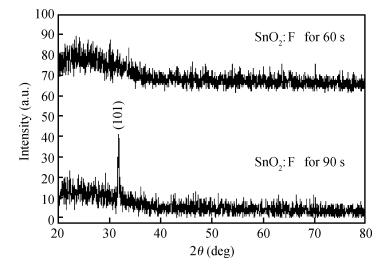
Fig. 1.
X-ray diffraction spectra of SnO2 : F thin films grown at two times. The films are deposited on a glass substrate at Ts=350 ℃.
SEMICONDUCTOR MATERIALS
Achour Rahal1, 2, Said Benramache1, 3 and Boubaker Benhaoua1
Corresponding author: Said Benramache, Email: saidzno2006@gmail.com
Abstract: We studied fluorine-doped tin oxide on a glass substrate at 350℃ using an ultrasonic spray technique. Tin (Ⅱ) chloride dehydrate, ammonium fluoride dehydrate, ethanol and NaOH were used as the starting material, dopant source, solvent and stabilizer, respectively. The SnO2:F thin films were deposited at 350℃ and a pending time of 60 and 90 s. The as-grown films exhibit a hexagonal wurtzite structure and have (101) orientation. The G=31.82 nm value of the grain size is attained from SnO2:F film grown at 90 s, and the transmittance is greater than 80% in the visible region. The optical gap energy is found to measure 4.05 eV for the film prepared at 90 s, and the increase in the electrical conductivity of the film with the temperature of the sample is up to a maximum value of 265.58 (Ω ·cm) -1, with the maximum activation energy value of the films being found to measure 22.85 meV, indicating that the films exhibit an n-type semiconducting nature.
Keywords: SnO2:F, thin film, TCO, ultrasonic spray technique
| [1] |
Gui T, Hao L, Wang J, et al. Structure and features of SnO2 thin films prepared by RF reactive sputtering. Chinese Optics Letters, 2010, 8(s1):134 doi: 10.3788/COL
|
| [2] |
Kwon J H, Choi Y H, Kim D H, et al. Orientation relationship of polycrystalline Pd-doped SnO2 thin film deposits on sapphire substrates. Thin Solid Films, 2008, 517(2):550 doi: 10.1016/j.tsf.2008.06.074
|
| [3] |
Jiménez V M, Espinós J P, Gonzaález-Elipe A R. Effect of texture and annealing treatments in SnO2 and Pd/SnO2 gas sensor materials. Sensors and Actuators B, 1999, 61(1-3):23 doi: 10.1016/S0925-4005(99)00275-0
|
| [4] |
Murakami K, Nakajima K, Kaneko S. Initial growth of SnO2 thin film on the glass substrate deposited by the spray pyrolysis technique. Thin Solid Films, 2007, 515(24):8632 doi: 10.1016/j.tsf.2007.03.128
|
| [5] |
Ghimbeu C M, Landschoot R C, Schoonman J, et al. Preparation and characterization of SnO2 and Cu-doped SnO2 thin films using electrostatic spray deposition (ESD). Journal of the European Ceramic Society, 2007, 27(1):207 doi: 10.1016/j.jeurceramsoc.2006.05.092
|
| [6] |
Chung J H, Choe Y S, Kim D S. Effect of low energy oxygen ion beam on optical and electrical characteristics of dual ion beam sputtered SnO2 thin films. Thin Solid Films, 1999, 349(1/2):126 doi: 10.1088/0268-1242/28/8/085014
|
| [7] |
Ohgaki T, Matsuokaa R, Watanabe K, et al. Synthesizing SnO2 thin films and characterizing sensing performances. Sensors and Actuators B, 2010, 150(1):99 doi: 10.1016/j.snb.2010.07.036
|
| [8] |
Leo G, Rella R, Siciliano P. Sprayed SnO2 thin films for NO2 sensors. Sensors and Actuators B, 1999, 58(1-3):370 doi: 10.1016/S0925-4005(99)00098-2
|
| [9] |
Yang T, Qin X, Wang H, et al. Preparation and application in p-n homojunction diode of p-type transparent conducting Ga-doped SnO2 thin films. Thin Solid Films, 2010, 518(19):5542 doi: 10.1016/j.tsf.2010.04.063
|
| [10] |
Ajili M, Castagné M, Turki N K. Study on the doping effect of Sn-doped ZnO thin films. Superlattices and Microstructures, 2013, 53(1):213 http://ieeexplore.ieee.org/abstract/document/7449374/?section=abstract
|
| [11] |
Benramache S, Benhaoua B, Chabane F. Effect of substrate temperature on the stability of transparent conducting cobalt doped ZnO thin films. Journal of Semiconductors, 2012, 33(9):093001 doi: 10.1088/1674-4926/33/9/093001
|
| [12] |
Benramache S, Benhaoua B, Chabane F, et al. Influence of growth time on crystalline structure, conductivity and optical properties of ZnO thin films. Journal of Semiconductors, 2013, 34(2):023001 doi: 10.1088/1674-4926/34/2/023001
|
| [13] |
Benramache S, Benhaoua B, Khechai N, et al. Elaboration and characterisation of ZnO thin films. Matériaux & Techniques, 2012, 100(6/7):573 http://www.wenkuxiazai.com/doc/2e70a31d10a6f524ccbf85a5.html
|
| [14] |
Benrabah B, Bouaza A, Kadari A, et al. Impedance studies of Sb doped SnO2 thin film prepared by sol gel process. Superlattices and Microstructures, 2011, 50(6):591 doi: 10.1016/j.spmi.2011.08.009
|
| [15] |
Benramache S, Benhaoua B. Influence of annealing temperature on structural and optical properties of ZnO:In thin films prepared by ultrasonic spray technique. Superlattices and Microstructures, 2012, 52(6):1062 doi: 10.1016/j.spmi.2012.08.006
|
| [16] |
Ilican S, Caglar Y, Caglar M, et al. Structural, optical and electrical properties of F-doped ZnO nanorod semiconductor thin films deposited by sol-gel process. Appl Surf Sci, 2008, 255(5):2353 doi: 10.1016/j.apsusc.2008.07.111
|
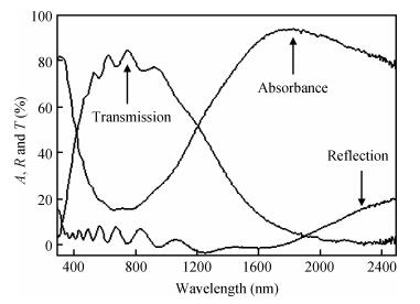
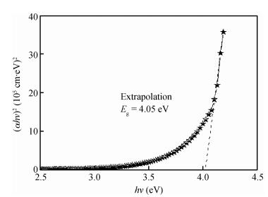
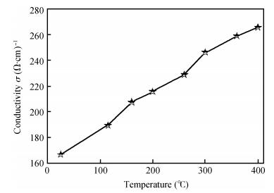
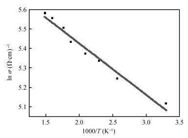
Table 1.
The Bragg angle

|
| [1] |
Gui T, Hao L, Wang J, et al. Structure and features of SnO2 thin films prepared by RF reactive sputtering. Chinese Optics Letters, 2010, 8(s1):134 doi: 10.3788/COL
|
| [2] |
Kwon J H, Choi Y H, Kim D H, et al. Orientation relationship of polycrystalline Pd-doped SnO2 thin film deposits on sapphire substrates. Thin Solid Films, 2008, 517(2):550 doi: 10.1016/j.tsf.2008.06.074
|
| [3] |
Jiménez V M, Espinós J P, Gonzaález-Elipe A R. Effect of texture and annealing treatments in SnO2 and Pd/SnO2 gas sensor materials. Sensors and Actuators B, 1999, 61(1-3):23 doi: 10.1016/S0925-4005(99)00275-0
|
| [4] |
Murakami K, Nakajima K, Kaneko S. Initial growth of SnO2 thin film on the glass substrate deposited by the spray pyrolysis technique. Thin Solid Films, 2007, 515(24):8632 doi: 10.1016/j.tsf.2007.03.128
|
| [5] |
Ghimbeu C M, Landschoot R C, Schoonman J, et al. Preparation and characterization of SnO2 and Cu-doped SnO2 thin films using electrostatic spray deposition (ESD). Journal of the European Ceramic Society, 2007, 27(1):207 doi: 10.1016/j.jeurceramsoc.2006.05.092
|
| [6] |
Chung J H, Choe Y S, Kim D S. Effect of low energy oxygen ion beam on optical and electrical characteristics of dual ion beam sputtered SnO2 thin films. Thin Solid Films, 1999, 349(1/2):126 doi: 10.1088/0268-1242/28/8/085014
|
| [7] |
Ohgaki T, Matsuokaa R, Watanabe K, et al. Synthesizing SnO2 thin films and characterizing sensing performances. Sensors and Actuators B, 2010, 150(1):99 doi: 10.1016/j.snb.2010.07.036
|
| [8] |
Leo G, Rella R, Siciliano P. Sprayed SnO2 thin films for NO2 sensors. Sensors and Actuators B, 1999, 58(1-3):370 doi: 10.1016/S0925-4005(99)00098-2
|
| [9] |
Yang T, Qin X, Wang H, et al. Preparation and application in p-n homojunction diode of p-type transparent conducting Ga-doped SnO2 thin films. Thin Solid Films, 2010, 518(19):5542 doi: 10.1016/j.tsf.2010.04.063
|
| [10] |
Ajili M, Castagné M, Turki N K. Study on the doping effect of Sn-doped ZnO thin films. Superlattices and Microstructures, 2013, 53(1):213 http://ieeexplore.ieee.org/abstract/document/7449374/?section=abstract
|
| [11] |
Benramache S, Benhaoua B, Chabane F. Effect of substrate temperature on the stability of transparent conducting cobalt doped ZnO thin films. Journal of Semiconductors, 2012, 33(9):093001 doi: 10.1088/1674-4926/33/9/093001
|
| [12] |
Benramache S, Benhaoua B, Chabane F, et al. Influence of growth time on crystalline structure, conductivity and optical properties of ZnO thin films. Journal of Semiconductors, 2013, 34(2):023001 doi: 10.1088/1674-4926/34/2/023001
|
| [13] |
Benramache S, Benhaoua B, Khechai N, et al. Elaboration and characterisation of ZnO thin films. Matériaux & Techniques, 2012, 100(6/7):573 http://www.wenkuxiazai.com/doc/2e70a31d10a6f524ccbf85a5.html
|
| [14] |
Benrabah B, Bouaza A, Kadari A, et al. Impedance studies of Sb doped SnO2 thin film prepared by sol gel process. Superlattices and Microstructures, 2011, 50(6):591 doi: 10.1016/j.spmi.2011.08.009
|
| [15] |
Benramache S, Benhaoua B. Influence of annealing temperature on structural and optical properties of ZnO:In thin films prepared by ultrasonic spray technique. Superlattices and Microstructures, 2012, 52(6):1062 doi: 10.1016/j.spmi.2012.08.006
|
| [16] |
Ilican S, Caglar Y, Caglar M, et al. Structural, optical and electrical properties of F-doped ZnO nanorod semiconductor thin films deposited by sol-gel process. Appl Surf Sci, 2008, 255(5):2353 doi: 10.1016/j.apsusc.2008.07.111
|


Article views: 4213 Times PDF downloads: 46 Times Cited by: 0 Times
Received: 08 January 2013 Revised: 13 February 2013 Online: Published: 01 August 2013
| Citation: |
Achour Rahal, Said Benramache, Boubaker Benhaoua. Preparation of n-type semiconductor SnO2 thin films[J]. Journal of Semiconductors, 2013, 34(8): 083002. doi: 10.1088/1674-4926/34/8/083002
****
A Rahal, S Benramache, B Benhaoua. Preparation of n-type semiconductor SnO2 thin films[J]. J. Semicond., 2013, 34(8): 083002. doi: 10.1088/1674-4926/34/8/083002.

|
| [1] |
Gui T, Hao L, Wang J, et al. Structure and features of SnO2 thin films prepared by RF reactive sputtering. Chinese Optics Letters, 2010, 8(s1):134 doi: 10.3788/COL
|
| [2] |
Kwon J H, Choi Y H, Kim D H, et al. Orientation relationship of polycrystalline Pd-doped SnO2 thin film deposits on sapphire substrates. Thin Solid Films, 2008, 517(2):550 doi: 10.1016/j.tsf.2008.06.074
|
| [3] |
Jiménez V M, Espinós J P, Gonzaález-Elipe A R. Effect of texture and annealing treatments in SnO2 and Pd/SnO2 gas sensor materials. Sensors and Actuators B, 1999, 61(1-3):23 doi: 10.1016/S0925-4005(99)00275-0
|
| [4] |
Murakami K, Nakajima K, Kaneko S. Initial growth of SnO2 thin film on the glass substrate deposited by the spray pyrolysis technique. Thin Solid Films, 2007, 515(24):8632 doi: 10.1016/j.tsf.2007.03.128
|
| [5] |
Ghimbeu C M, Landschoot R C, Schoonman J, et al. Preparation and characterization of SnO2 and Cu-doped SnO2 thin films using electrostatic spray deposition (ESD). Journal of the European Ceramic Society, 2007, 27(1):207 doi: 10.1016/j.jeurceramsoc.2006.05.092
|
| [6] |
Chung J H, Choe Y S, Kim D S. Effect of low energy oxygen ion beam on optical and electrical characteristics of dual ion beam sputtered SnO2 thin films. Thin Solid Films, 1999, 349(1/2):126 doi: 10.1088/0268-1242/28/8/085014
|
| [7] |
Ohgaki T, Matsuokaa R, Watanabe K, et al. Synthesizing SnO2 thin films and characterizing sensing performances. Sensors and Actuators B, 2010, 150(1):99 doi: 10.1016/j.snb.2010.07.036
|
| [8] |
Leo G, Rella R, Siciliano P. Sprayed SnO2 thin films for NO2 sensors. Sensors and Actuators B, 1999, 58(1-3):370 doi: 10.1016/S0925-4005(99)00098-2
|
| [9] |
Yang T, Qin X, Wang H, et al. Preparation and application in p-n homojunction diode of p-type transparent conducting Ga-doped SnO2 thin films. Thin Solid Films, 2010, 518(19):5542 doi: 10.1016/j.tsf.2010.04.063
|
| [10] |
Ajili M, Castagné M, Turki N K. Study on the doping effect of Sn-doped ZnO thin films. Superlattices and Microstructures, 2013, 53(1):213 http://ieeexplore.ieee.org/abstract/document/7449374/?section=abstract
|
| [11] |
Benramache S, Benhaoua B, Chabane F. Effect of substrate temperature on the stability of transparent conducting cobalt doped ZnO thin films. Journal of Semiconductors, 2012, 33(9):093001 doi: 10.1088/1674-4926/33/9/093001
|
| [12] |
Benramache S, Benhaoua B, Chabane F, et al. Influence of growth time on crystalline structure, conductivity and optical properties of ZnO thin films. Journal of Semiconductors, 2013, 34(2):023001 doi: 10.1088/1674-4926/34/2/023001
|
| [13] |
Benramache S, Benhaoua B, Khechai N, et al. Elaboration and characterisation of ZnO thin films. Matériaux & Techniques, 2012, 100(6/7):573 http://www.wenkuxiazai.com/doc/2e70a31d10a6f524ccbf85a5.html
|
| [14] |
Benrabah B, Bouaza A, Kadari A, et al. Impedance studies of Sb doped SnO2 thin film prepared by sol gel process. Superlattices and Microstructures, 2011, 50(6):591 doi: 10.1016/j.spmi.2011.08.009
|
| [15] |
Benramache S, Benhaoua B. Influence of annealing temperature on structural and optical properties of ZnO:In thin films prepared by ultrasonic spray technique. Superlattices and Microstructures, 2012, 52(6):1062 doi: 10.1016/j.spmi.2012.08.006
|
| [16] |
Ilican S, Caglar Y, Caglar M, et al. Structural, optical and electrical properties of F-doped ZnO nanorod semiconductor thin films deposited by sol-gel process. Appl Surf Sci, 2008, 255(5):2353 doi: 10.1016/j.apsusc.2008.07.111
|

 WeChat ID
Journal of Semiconductors © 2017 All Rights Reserved 京ICP备05085259号-2

 DownLoad:

