1. Key Laboratory of Display Material and Photoelectric Devices(Ministry of Education) and School of Materials Science and Engineering, Tianjin Key Laboratory of Photoelectric Materials and Devices, Tianjin University of Technology, Tianjin 300384, ChinaKey Laboratory of Display Material and Photoelectric Devices(Ministry of Education) and School of Materials Science and Engineering, Tianjin Key Laboratory of Photoelectric Materials and Devices, Tianjin University of Technology, Tianjin 300384, China
2. School of Science, Tianjin University of Technology, Tianjin 300384, ChinaSchool of Science, Tianjin University of Technology, Tianjin 300384, China
Abstract: We investigated the properties of C60-based organic field-effect transistors (OFETs) with a pentacene passivation layer inserted between the C60 active layer and the gate dielectric. After modification of the pentacene passivation layer, the performance of the devices was considerably improved compared to C60-based OFETs with only a PMMA dielectric. The peak field-effect mobility was up to 1.01 cm2/(V·s) and the on/off ratio shifted to 104. This result indicates that using a pentacene passivation layer is an effective way to improve the performance of N-type OFETs.
Organic field-effect transistors (OFETs) have attracted considerable attention because of their prominent features for realizing low-cost, large-area, mechanically flexible, and lightweight devices[1-6]. The performance of OFETs has been improved rapidly in the last two decade. So far, much effort has focused on researching P-type OFETs, but only a few N-type OFETs have been reported[7-9]. The most probable reason for this is that N-type material is relative unstable, and sensitive to oxygen and humidity[10, 11]. In order to realize applications, such as in organic complementary logic circuits, both P-type and N-type transistors are needed and should have comparable performance[12]. Therefore, further research is still needed to establish N-type OFETs in organic electronics.
Among N-type organic semiconductors, fullerenes hold great promise for high-mobility n-channel OFETs. Since the first report by Haddon et al.[13] in 1995, improvements in the processing of C60 have led to the demonstration of the highest electron mobility of 6 cm2/(V⋅s) by Anthopoulos et al.[14] in C60 films deposited by hot wall epitaxy at an elevated temperature of 250 ℃. By modifying the properties of the C60/SiO2 interface using pentacene, Itaka et al.[15] obtained an electron mobility of 4.9 cm2/(V⋅s) in devices processed at 50 ℃ and tested in high vacuum, and the devices exhibited an ambipolar property due to the presence of the pentacene wetting layer. Though their devices possess high mobilities, the fabrication needs special conditions. Thus common experience methods, such as thermal evaporation, are required to achieve N-type OFETs.
In general, the performance of OFETs is not governed solely by the materials or structural options, whereas it is largely influenced by the interface modified layers. It is well known that OFETs work in the accumulation region, and that most of the modulated charge lies in the semiconductor near the semiconductor/dielectric interface. The interaction between the gate dielectric and the semiconductor layer plays an important role in the formation of carrier transport. So far, many groups have reported different methods to modify semiconductor/dielectric interfaces, including introducing an ultrathin polymer passivation[16] and inserting a small molecule material thin film[17], and so on. However, further research is still of great significance because it is difficult to provide a simple and effective way to improve the morphology of the semiconductor and to fill the traps of the gate dielectric to make the devices available for real applications.
In this paper, we demonstrate top-contact C60-based OFETs by inserting a pentacene passivation layer between C60 and the gate dielectric. After the modification of the 2 nm pentacene passivation layer, the enhanced performance is observed. The peak field-effect mobility is up to 1.01 cm2/(V⋅s) and the on/off ratio shifts to 104.
2.
Experiment
Figure 1(a) shows a schematic diagram of C60-based OFETs. Figures 1(b) and 1(c) show the molecular structures of pentacene and C60, respectively. The devices were prepared on indium-tin-oxide (ITO)-coated glass as the gate electrode and substrate. The substrate was cleaned with deionized water, acetone, and isopropanol in turn, and then a spin-coating 390 nm polymethyl methacrylate (PMMA) was used as the gate dielectric. The substrates with PMMA were transferred to a glove box and annealed on a hot plate at 120 ℃ for 2 h. An ultrathin pentacene passivation layer was thermally deposited first with a deposition rate of approximately 0.3 Å/s. In succession, a 40 nm C60 thin film was thermally evaporated at a deposition rate of 0.6 Å/s. Finally, the 150 nm Al source and drain electrodes were thermally evaporated through a shadow mask. The channel length (L) and width (W) were 80 μm and 4 mm, respectively, and all of the organic layers and source-drain electrodes were grown at a base pressure of 10−4 Pa. The electrical characteristics were measured using two Keithley 2400 source meters and a Keithley 485 picoammeter at room temperature under ambient atmosphere conditions.
Figure
1.
(a) Schematic diagram of a C60-based OFET with a pentacene passivation layer. (b) The molecular structure of pentacene. (c) The molecular structure of C60.
Figures 2(a) and 2(b) show the output and transfer characteristics, respectively, of C60 OFETs without the pentacene passivation layer. Though the linear and saturation regions are observed with the increase in drain voltage (Vds), the output current is only is 1.18 × 10⁻⁵ A at a 60 V gate voltage (Vg). Figures 3(a) and 3(b) show the electrical characteristics of the devices with a 2 nm thick pentacene passivation layer. The device exhibits typical n-channel operational characteristics, and the smooth Ids-Vds curves are observed. When the gate voltage (Vg) is kept at 60 V, the output current (Ids) reaches 4.13 × 10⁻⁴ A. Compared with the bare interlayer, the output current (Ids) values are higher by more than one order of magnitude.
The field-effect mobility (μ) of the device may be estimated from the relation between the saturated source-drain current Ids and Vg,
Ids=W2LμCi(Vg−Vth)2.
(1)
Figure
2.
The (a) output and (b) transfer characteristics of C60 OFETs.
Here, W represents the channel width, L the channel length, μ the field-effect mobility, and Ci the gate capacitance per unit area of the PMMA dielectric. The capacitance value of the PMMA insulator is 6.81 nF/cm2. Vg is the gate voltage, Vth is the threshold voltage, and Ids is the saturated drain current. Using Eq. (1), the saturated field-effect mobility of the device with the PMMA-only dielectric can be calculated to be 2.13 × 10⁻¹ cm2/(V⋅s). After incorporating with 2 nm pentacene passivation, the peak field-effect mobility reached 1.01 cm2/(V⋅s). But when the thickness of the pentacene passivation layer was more than 2 nm, the saturated field-effect mobility of the device began to decline. The results indicate that the field-effect mobility of the device increases as the thickness of the pentacene passivation layer increases from 0 to 2 nm, and then decreases as the pentacene passivation layer thickness increases to 4 nm, as shown in Fig. 4. This variety in the field-effect mobility reveals that N-type transport is enhanced with the optimized thickness of the pentacene passivation layer. Table 1 shows a summary of the performance parameters for the devices with and without the pentacene passivation layer. This means that the pentacene passivation layer plays a key role in the performance of the device.
Figure
4.
The field-effect mobility of the device with different thicknesses of pentacene passivation layer.
In order to understand the enhancement of the device mobility, the surface morphologies of the C60 films with and without a pentacene passivation layer were examined by an atomic force microscope (AFM). Figures 5(a) and 5(b) show AFM images of C60 (40 nm)/PMMA and C60 (40 nm)/pentacene (2 nm)/PMMA films, respectively. As shown in Fig. 5(b), the larger C60 grain size is observed. The grains grow to an average size of about 106 nm in the 1 μm square area, which indicates that the grain boundary is seriously decreased. Usually, many traps are concentrated on the grain boundary, which can capture the charge carriers. At this point, the larger grain size of the C60 film on the pentacene passivation layer should have less of a grain boundary, leading to fewer traps. Thus, a lower grain boundary can transport carrier charges more easily and the field-effect mobility of the devices is improved.
Figure
5.
Atomic force microscopy images in 1 × 1 μm2 of (a) C60 (40 nm)/PMMA and (b) C60 (40 nm)/pentacene (2 nm)/PMMA.
Based on the above results, after inserting the pentacene passivation layer, we consider that two reasons can influence the performance of the devices. One may be that the pentacene passivation layer can reduce charge trapping to make the charge carriers easier to transport. The other is that the morphology and crystallinity of the C60 film can be changed, and then charge carrier transport can be improved.
4.
Conclusion
In summary, we demonstrated the effect of a pentacene passivation layer between the C60 active layer and the gate dielectric in N-type OFETs. The device performance can be enhanced by modifying the pentacene passivation layer. A high electron mobility of up to 1.01 cm2/(V⋅s) and on-off ratio of 104 were obtained. The increase in the C60 film grain size with the insertion of a pentacene passivation layer is believed to be the reason for the improved performance. Therefore, using a pentacene passivation layer is an effective and simple method to prepare high-performance n-channel transistors for practical application.
References
[1]
Tsumura A, Koezuka H, Ando T. Macromolecular electronic device:field-effect transistor with a polythiophene thin film. Appl Phys Lett, 1986, 49(18):1210 doi: 10.1063/1.97417
[2]
Zhao G, Cheng X M, Tian H J, et al. Improved performance of pentacene organic field-effect transistors by inserting a V2O5 metal oxide layer. Chin Phys Lett, 2011, 28(12):127203 doi: 10.1088/0256-307X/28/12/127203
[3]
Akimichi H, Waragai K, Hotta S, et al. Field-effect transistors using alkyl substituted oligothiophenes. Appl Phys Lett, 1991, 58(14):1500 doi: 10.1063/1.105158
[4]
Minagawa M, Higashikawa T, Nakai K, et al. Fabrication and evaluation of poly (3-hexylthiophene) field-effect transistor with V2O5 layer. Molecular Crystals and Liquid Crystals, 2010, 519(1):213 doi: 10.1080/15421401003597977
[5]
Yadav S, Kumar P, Ghosh S. Optimization of surface morphology to reduce the effect of grain boundaries and contact resistance in small molecule based thin film transistors. Appl Phys Lett, 2012, 101(19):193307 doi: 10.1063/1.4766913
[6]
Dimitrakopoulos C D, Malenfant P R L. Organic thin film transistors for large area electronics. Adv Mater, 2002, 14(2):99 doi: 10.1002/(ISSN)1521-4095
[7]
Newman C R, Frisbie C D, da Silva Filho D A, et al. Introduction to organic thin film transistors and design of n-channel organic semiconductors. Chem Mater, 2004, 16(23):4436 doi: 10.1021/cm049391x
[8]
Chua L L, Zaumseil J, Chang J F, et al. General observation of n-type field-effect behaviour in organic semiconductors. Nature, 2005, 434(7030):194 doi: 10.1038/nature03376
[9]
Zheng Hong, Cheng Xiaoman, Tian Haijun, et al. Enhanced performance of C60 organic field effect transistors using a tris (8-hydroxyquinoline) aluminum buffer layer. Journal of Semiconductors, 2011, 32(9):094005 doi: 10.1088/1674-4926/32/9/094005
[10]
Kao C C, Lin P, Lee C C, et al. High-performance bottom-contact devices based on an air-stable n-type organic semiconductor N, N-bis (4-trifluoromethoxybenzyl)-1, 4, 5, 8-naphthalene-tetracarboxylic di-imide. Appl Phys Lett, 2007, 90:212101 doi: 10.1063/1.2741414
[11]
Wang S, Minari T, Miyadera T, et al. Contact-metal dependent current injection in pentacene thin-film transistors. Appl Phys Lett, 2007, 91(20):203508 doi: 10.1063/1.2813640
[12]
Zhou Jianlin, Niu Qiaoli. Properties of C60 thin film transistor based on polystyrene. Chin Phys B, 2010, 19(7):077305 doi: 10.1088/1674-1056/19/7/077305
[13]
Haddon R, Perel A, Morris R, et al. C60 thin film transistors. Appl Phys Lett, 1995, 67(1):121 doi: 10.1063/1.115503
[14]
Anthopoulos T D, Singh B, Marjanovic N, et al. High performance n-channel organic field-effect transistors and ring oscillators based on C60 fullerene films. Appl Phys Lett, 2006, 89(21):213504 doi: 10.1063/1.2387892
[15]
Itaka K, Yamashiro M, Yamaguchi J, et al. High-mobility C60 field-effect transistors fabricated on molecular-wetting controlled substrates. Adv Mater, 2006, 18(13):1713 doi: 10.1002/(ISSN)1521-4095
[16]
Lee H N, Lee Y G, Ko I H, et al. Organic passivation layers for pentacene organic thin-film transistors. Current Appl Phys, 2008, 8(5):626 doi: 10.1016/j.cap.2007.11.003
[17]
Zhou Jianlin, Yu Junsheng, Yu Xinge, et al. A high mobility C60 field-effect transistor with an ultrathin pentacene passivation layer and bathophenanthroline/metal bilayer electrodes. Chin Phys B, 2012, 21(2):027305 doi: 10.1088/1674-1056/21/2/027305
Fig. 1.
(a) Schematic diagram of a C60-based OFET with a pentacene passivation layer. (b) The molecular structure of pentacene. (c) The molecular structure of C60.
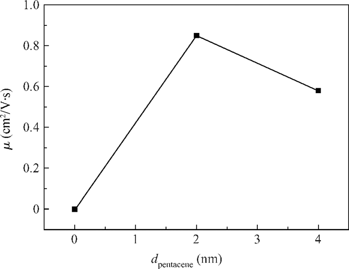
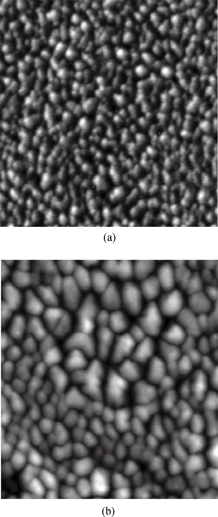
Table 1.
Summary of the performance parameters for devices with and without the pentacene passivation layer.
[1]
Tsumura A, Koezuka H, Ando T. Macromolecular electronic device:field-effect transistor with a polythiophene thin film. Appl Phys Lett, 1986, 49(18):1210 doi: 10.1063/1.97417
[2]
Zhao G, Cheng X M, Tian H J, et al. Improved performance of pentacene organic field-effect transistors by inserting a V2O5 metal oxide layer. Chin Phys Lett, 2011, 28(12):127203 doi: 10.1088/0256-307X/28/12/127203
[3]
Akimichi H, Waragai K, Hotta S, et al. Field-effect transistors using alkyl substituted oligothiophenes. Appl Phys Lett, 1991, 58(14):1500 doi: 10.1063/1.105158
[4]
Minagawa M, Higashikawa T, Nakai K, et al. Fabrication and evaluation of poly (3-hexylthiophene) field-effect transistor with V2O5 layer. Molecular Crystals and Liquid Crystals, 2010, 519(1):213 doi: 10.1080/15421401003597977
[5]
Yadav S, Kumar P, Ghosh S. Optimization of surface morphology to reduce the effect of grain boundaries and contact resistance in small molecule based thin film transistors. Appl Phys Lett, 2012, 101(19):193307 doi: 10.1063/1.4766913
[6]
Dimitrakopoulos C D, Malenfant P R L. Organic thin film transistors for large area electronics. Adv Mater, 2002, 14(2):99 doi: 10.1002/(ISSN)1521-4095
[7]
Newman C R, Frisbie C D, da Silva Filho D A, et al. Introduction to organic thin film transistors and design of n-channel organic semiconductors. Chem Mater, 2004, 16(23):4436 doi: 10.1021/cm049391x
[8]
Chua L L, Zaumseil J, Chang J F, et al. General observation of n-type field-effect behaviour in organic semiconductors. Nature, 2005, 434(7030):194 doi: 10.1038/nature03376
[9]
Zheng Hong, Cheng Xiaoman, Tian Haijun, et al. Enhanced performance of C60 organic field effect transistors using a tris (8-hydroxyquinoline) aluminum buffer layer. Journal of Semiconductors, 2011, 32(9):094005 doi: 10.1088/1674-4926/32/9/094005
[10]
Kao C C, Lin P, Lee C C, et al. High-performance bottom-contact devices based on an air-stable n-type organic semiconductor N, N-bis (4-trifluoromethoxybenzyl)-1, 4, 5, 8-naphthalene-tetracarboxylic di-imide. Appl Phys Lett, 2007, 90:212101 doi: 10.1063/1.2741414
[11]
Wang S, Minari T, Miyadera T, et al. Contact-metal dependent current injection in pentacene thin-film transistors. Appl Phys Lett, 2007, 91(20):203508 doi: 10.1063/1.2813640
[12]
Zhou Jianlin, Niu Qiaoli. Properties of C60 thin film transistor based on polystyrene. Chin Phys B, 2010, 19(7):077305 doi: 10.1088/1674-1056/19/7/077305
[13]
Haddon R, Perel A, Morris R, et al. C60 thin film transistors. Appl Phys Lett, 1995, 67(1):121 doi: 10.1063/1.115503
[14]
Anthopoulos T D, Singh B, Marjanovic N, et al. High performance n-channel organic field-effect transistors and ring oscillators based on C60 fullerene films. Appl Phys Lett, 2006, 89(21):213504 doi: 10.1063/1.2387892
[15]
Itaka K, Yamashiro M, Yamaguchi J, et al. High-mobility C60 field-effect transistors fabricated on molecular-wetting controlled substrates. Adv Mater, 2006, 18(13):1713 doi: 10.1002/(ISSN)1521-4095
[16]
Lee H N, Lee Y G, Ko I H, et al. Organic passivation layers for pentacene organic thin-film transistors. Current Appl Phys, 2008, 8(5):626 doi: 10.1016/j.cap.2007.11.003
[17]
Zhou Jianlin, Yu Junsheng, Yu Xinge, et al. A high mobility C60 field-effect transistor with an ultrathin pentacene passivation layer and bathophenanthroline/metal bilayer electrodes. Chin Phys B, 2012, 21(2):027305 doi: 10.1088/1674-1056/21/2/027305
Li Hongjian, Ouyang Jun, Dai Guozhang, Dai Xiaoyu, Pan Yanzhi, et al.
Chinese Journal of Semiconductors , 2006, 27(4): 674-678.
Search
GET CITATION
Xiaoyu Liang, Xiaoman Cheng, Boqun Du, Xiao Bai, Jianfeng Fan. Enhanced performance of C60 N-type organic field-effect transistors using a pentacene passivation layer[J]. Journal of Semiconductors, 2013, 34(8): 084002. doi: 10.1088/1674-4926/34/8/084002
X Y Liang, X M Cheng, B Q Du, X Bai, J F Fan. Enhanced performance of C60 N-type organic field-effect transistors using a pentacene passivation layer[J]. J. Semicond., 2013, 34(8): 084002. doi: 10.1088/1674-4926/34/8/084002.
Export: BibTexEndNote
Share:
Article Metrics
Article views: 2374 TimesPDF downloads: 11 TimesCited by: 0 Times
History
Received: 02 January 2013Revised: 29 March 2013Online:Published: 01 August 2013
Xiaoyu Liang, Xiaoman Cheng, Boqun Du, Xiao Bai, Jianfeng Fan. Enhanced performance of C60 N-type organic field-effect transistors using a pentacene passivation layer[J]. Journal of Semiconductors, 2013, 34(8): 084002. doi: 10.1088/1674-4926/34/8/084002 ****X Y Liang, X M Cheng, B Q Du, X Bai, J F Fan. Enhanced performance of C60 N-type organic field-effect transistors using a pentacene passivation layer[J]. J. Semicond., 2013, 34(8): 084002. doi: 10.1088/1674-4926/34/8/084002.
Citation:
Xiaoyu Liang, Xiaoman Cheng, Boqun Du, Xiao Bai, Jianfeng Fan. Enhanced performance of C60 N-type organic field-effect transistors using a pentacene passivation layer[J]. Journal of Semiconductors, 2013, 34(8): 084002. doi: 10.1088/1674-4926/34/8/084002
****
X Y Liang, X M Cheng, B Q Du, X Bai, J F Fan. Enhanced performance of C60 N-type organic field-effect transistors using a pentacene passivation layer[J]. J. Semicond., 2013, 34(8): 084002. doi: 10.1088/1674-4926/34/8/084002.
Key Laboratory of Display Material and Photoelectric Devices(Ministry of Education) and School of Materials Science and Engineering, Tianjin Key Laboratory of Photoelectric Materials and Devices, Tianjin University of Technology, Tianjin 300384, China
2.
School of Science, Tianjin University of Technology, Tianjin 300384, China
Funds:
the National Natural Science Foundation of China61076065
the Natural Science Foundation of Tianjin City, China07JCYBJC12700
Project supported by the National Natural Science Foundation of China (No. 61076065) and the Natural Science Foundation of Tianjin City, China (No. 07JCYBJC12700)
We investigated the properties of C60-based organic field-effect transistors (OFETs) with a pentacene passivation layer inserted between the C60 active layer and the gate dielectric. After modification of the pentacene passivation layer, the performance of the devices was considerably improved compared to C60-based OFETs with only a PMMA dielectric. The peak field-effect mobility was up to 1.01 cm2/(V·s) and the on/off ratio shifted to 104. This result indicates that using a pentacene passivation layer is an effective way to improve the performance of N-type OFETs.
Organic field-effect transistors (OFETs) have attracted considerable attention because of their prominent features for realizing low-cost, large-area, mechanically flexible, and lightweight devices[1-6]. The performance of OFETs has been improved rapidly in the last two decade. So far, much effort has focused on researching P-type OFETs, but only a few N-type OFETs have been reported[7-9]. The most probable reason for this is that N-type material is relative unstable, and sensitive to oxygen and humidity[10, 11]. In order to realize applications, such as in organic complementary logic circuits, both P-type and N-type transistors are needed and should have comparable performance[12]. Therefore, further research is still needed to establish N-type OFETs in organic electronics.
Among N-type organic semiconductors, fullerenes hold great promise for high-mobility n-channel OFETs. Since the first report by Haddon et al.[13] in 1995, improvements in the processing of C60 have led to the demonstration of the highest electron mobility of 6 cm2/(V⋅s) by Anthopoulos et al.[14] in C60 films deposited by hot wall epitaxy at an elevated temperature of 250 ℃. By modifying the properties of the C60/SiO2 interface using pentacene, Itaka et al.[15] obtained an electron mobility of 4.9 cm2/(V⋅s) in devices processed at 50 ℃ and tested in high vacuum, and the devices exhibited an ambipolar property due to the presence of the pentacene wetting layer. Though their devices possess high mobilities, the fabrication needs special conditions. Thus common experience methods, such as thermal evaporation, are required to achieve N-type OFETs.
In general, the performance of OFETs is not governed solely by the materials or structural options, whereas it is largely influenced by the interface modified layers. It is well known that OFETs work in the accumulation region, and that most of the modulated charge lies in the semiconductor near the semiconductor/dielectric interface. The interaction between the gate dielectric and the semiconductor layer plays an important role in the formation of carrier transport. So far, many groups have reported different methods to modify semiconductor/dielectric interfaces, including introducing an ultrathin polymer passivation[16] and inserting a small molecule material thin film[17], and so on. However, further research is still of great significance because it is difficult to provide a simple and effective way to improve the morphology of the semiconductor and to fill the traps of the gate dielectric to make the devices available for real applications.
In this paper, we demonstrate top-contact C60-based OFETs by inserting a pentacene passivation layer between C60 and the gate dielectric. After the modification of the 2 nm pentacene passivation layer, the enhanced performance is observed. The peak field-effect mobility is up to 1.01 cm2/(V⋅s) and the on/off ratio shifts to 104.
2.
Experiment
Figure 1(a) shows a schematic diagram of C60-based OFETs. Figures 1(b) and 1(c) show the molecular structures of pentacene and C60, respectively. The devices were prepared on indium-tin-oxide (ITO)-coated glass as the gate electrode and substrate. The substrate was cleaned with deionized water, acetone, and isopropanol in turn, and then a spin-coating 390 nm polymethyl methacrylate (PMMA) was used as the gate dielectric. The substrates with PMMA were transferred to a glove box and annealed on a hot plate at 120 ℃ for 2 h. An ultrathin pentacene passivation layer was thermally deposited first with a deposition rate of approximately 0.3 Å/s. In succession, a 40 nm C60 thin film was thermally evaporated at a deposition rate of 0.6 Å/s. Finally, the 150 nm Al source and drain electrodes were thermally evaporated through a shadow mask. The channel length (L) and width (W) were 80 μm and 4 mm, respectively, and all of the organic layers and source-drain electrodes were grown at a base pressure of 10−4 Pa. The electrical characteristics were measured using two Keithley 2400 source meters and a Keithley 485 picoammeter at room temperature under ambient atmosphere conditions.
Figure
1.
(a) Schematic diagram of a C60-based OFET with a pentacene passivation layer. (b) The molecular structure of pentacene. (c) The molecular structure of C60.
Figures 2(a) and 2(b) show the output and transfer characteristics, respectively, of C60 OFETs without the pentacene passivation layer. Though the linear and saturation regions are observed with the increase in drain voltage (Vds), the output current is only is 1.18 × 10⁻⁵ A at a 60 V gate voltage (Vg). Figures 3(a) and 3(b) show the electrical characteristics of the devices with a 2 nm thick pentacene passivation layer. The device exhibits typical n-channel operational characteristics, and the smooth Ids-Vds curves are observed. When the gate voltage (Vg) is kept at 60 V, the output current (Ids) reaches 4.13 × 10⁻⁴ A. Compared with the bare interlayer, the output current (Ids) values are higher by more than one order of magnitude.
The field-effect mobility (μ) of the device may be estimated from the relation between the saturated source-drain current Ids and Vg,
Here, W represents the channel width, L the channel length, μ the field-effect mobility, and Ci the gate capacitance per unit area of the PMMA dielectric. The capacitance value of the PMMA insulator is 6.81 nF/cm2. Vg is the gate voltage, Vth is the threshold voltage, and Ids is the saturated drain current. Using Eq. (1), the saturated field-effect mobility of the device with the PMMA-only dielectric can be calculated to be 2.13 × 10⁻¹ cm2/(V⋅s). After incorporating with 2 nm pentacene passivation, the peak field-effect mobility reached 1.01 cm2/(V⋅s). But when the thickness of the pentacene passivation layer was more than 2 nm, the saturated field-effect mobility of the device began to decline. The results indicate that the field-effect mobility of the device increases as the thickness of the pentacene passivation layer increases from 0 to 2 nm, and then decreases as the pentacene passivation layer thickness increases to 4 nm, as shown in Fig. 4. This variety in the field-effect mobility reveals that N-type transport is enhanced with the optimized thickness of the pentacene passivation layer. Table 1 shows a summary of the performance parameters for the devices with and without the pentacene passivation layer. This means that the pentacene passivation layer plays a key role in the performance of the device.
Figure
4.
The field-effect mobility of the device with different thicknesses of pentacene passivation layer.
In order to understand the enhancement of the device mobility, the surface morphologies of the C60 films with and without a pentacene passivation layer were examined by an atomic force microscope (AFM). Figures 5(a) and 5(b) show AFM images of C60 (40 nm)/PMMA and C60 (40 nm)/pentacene (2 nm)/PMMA films, respectively. As shown in Fig. 5(b), the larger C60 grain size is observed. The grains grow to an average size of about 106 nm in the 1 μm square area, which indicates that the grain boundary is seriously decreased. Usually, many traps are concentrated on the grain boundary, which can capture the charge carriers. At this point, the larger grain size of the C60 film on the pentacene passivation layer should have less of a grain boundary, leading to fewer traps. Thus, a lower grain boundary can transport carrier charges more easily and the field-effect mobility of the devices is improved.
Figure
5.
Atomic force microscopy images in 1 × 1 μm2 of (a) C60 (40 nm)/PMMA and (b) C60 (40 nm)/pentacene (2 nm)/PMMA.
Based on the above results, after inserting the pentacene passivation layer, we consider that two reasons can influence the performance of the devices. One may be that the pentacene passivation layer can reduce charge trapping to make the charge carriers easier to transport. The other is that the morphology and crystallinity of the C60 film can be changed, and then charge carrier transport can be improved.
4.
Conclusion
In summary, we demonstrated the effect of a pentacene passivation layer between the C60 active layer and the gate dielectric in N-type OFETs. The device performance can be enhanced by modifying the pentacene passivation layer. A high electron mobility of up to 1.01 cm2/(V⋅s) and on-off ratio of 104 were obtained. The increase in the C60 film grain size with the insertion of a pentacene passivation layer is believed to be the reason for the improved performance. Therefore, using a pentacene passivation layer is an effective and simple method to prepare high-performance n-channel transistors for practical application.
Tsumura A, Koezuka H, Ando T. Macromolecular electronic device:field-effect transistor with a polythiophene thin film. Appl Phys Lett, 1986, 49(18):1210 doi: 10.1063/1.97417
[2]
Zhao G, Cheng X M, Tian H J, et al. Improved performance of pentacene organic field-effect transistors by inserting a V2O5 metal oxide layer. Chin Phys Lett, 2011, 28(12):127203 doi: 10.1088/0256-307X/28/12/127203
[3]
Akimichi H, Waragai K, Hotta S, et al. Field-effect transistors using alkyl substituted oligothiophenes. Appl Phys Lett, 1991, 58(14):1500 doi: 10.1063/1.105158
[4]
Minagawa M, Higashikawa T, Nakai K, et al. Fabrication and evaluation of poly (3-hexylthiophene) field-effect transistor with V2O5 layer. Molecular Crystals and Liquid Crystals, 2010, 519(1):213 doi: 10.1080/15421401003597977
[5]
Yadav S, Kumar P, Ghosh S. Optimization of surface morphology to reduce the effect of grain boundaries and contact resistance in small molecule based thin film transistors. Appl Phys Lett, 2012, 101(19):193307 doi: 10.1063/1.4766913
[6]
Dimitrakopoulos C D, Malenfant P R L. Organic thin film transistors for large area electronics. Adv Mater, 2002, 14(2):99 doi: 10.1002/(ISSN)1521-4095
[7]
Newman C R, Frisbie C D, da Silva Filho D A, et al. Introduction to organic thin film transistors and design of n-channel organic semiconductors. Chem Mater, 2004, 16(23):4436 doi: 10.1021/cm049391x
[8]
Chua L L, Zaumseil J, Chang J F, et al. General observation of n-type field-effect behaviour in organic semiconductors. Nature, 2005, 434(7030):194 doi: 10.1038/nature03376
[9]
Zheng Hong, Cheng Xiaoman, Tian Haijun, et al. Enhanced performance of C60 organic field effect transistors using a tris (8-hydroxyquinoline) aluminum buffer layer. Journal of Semiconductors, 2011, 32(9):094005 doi: 10.1088/1674-4926/32/9/094005
[10]
Kao C C, Lin P, Lee C C, et al. High-performance bottom-contact devices based on an air-stable n-type organic semiconductor N, N-bis (4-trifluoromethoxybenzyl)-1, 4, 5, 8-naphthalene-tetracarboxylic di-imide. Appl Phys Lett, 2007, 90:212101 doi: 10.1063/1.2741414
[11]
Wang S, Minari T, Miyadera T, et al. Contact-metal dependent current injection in pentacene thin-film transistors. Appl Phys Lett, 2007, 91(20):203508 doi: 10.1063/1.2813640
[12]
Zhou Jianlin, Niu Qiaoli. Properties of C60 thin film transistor based on polystyrene. Chin Phys B, 2010, 19(7):077305 doi: 10.1088/1674-1056/19/7/077305
[13]
Haddon R, Perel A, Morris R, et al. C60 thin film transistors. Appl Phys Lett, 1995, 67(1):121 doi: 10.1063/1.115503
[14]
Anthopoulos T D, Singh B, Marjanovic N, et al. High performance n-channel organic field-effect transistors and ring oscillators based on C60 fullerene films. Appl Phys Lett, 2006, 89(21):213504 doi: 10.1063/1.2387892
[15]
Itaka K, Yamashiro M, Yamaguchi J, et al. High-mobility C60 field-effect transistors fabricated on molecular-wetting controlled substrates. Adv Mater, 2006, 18(13):1713 doi: 10.1002/(ISSN)1521-4095
[16]
Lee H N, Lee Y G, Ko I H, et al. Organic passivation layers for pentacene organic thin-film transistors. Current Appl Phys, 2008, 8(5):626 doi: 10.1016/j.cap.2007.11.003
[17]
Zhou Jianlin, Yu Junsheng, Yu Xinge, et al. A high mobility C60 field-effect transistor with an ultrathin pentacene passivation layer and bathophenanthroline/metal bilayer electrodes. Chin Phys B, 2012, 21(2):027305 doi: 10.1088/1674-1056/21/2/027305
Xiaoyu Liang, Xiaoman Cheng, Boqun Du, Xiao Bai, Jianfeng Fan. Enhanced performance of C60 N-type organic field-effect transistors using a pentacene passivation layer[J]. Journal of Semiconductors, 2013, 34(8): 084002. doi: 10.1088/1674-4926/34/8/084002 ****X Y Liang, X M Cheng, B Q Du, X Bai, J F Fan. Enhanced performance of C60 N-type organic field-effect transistors using a pentacene passivation layer[J]. J. Semicond., 2013, 34(8): 084002. doi: 10.1088/1674-4926/34/8/084002.
Xiaoyu Liang, Xiaoman Cheng, Boqun Du, Xiao Bai, Jianfeng Fan. Enhanced performance of C60 N-type organic field-effect transistors using a pentacene passivation layer[J]. Journal of Semiconductors, 2013, 34(8): 084002. doi: 10.1088/1674-4926/34/8/084002
****
X Y Liang, X M Cheng, B Q Du, X Bai, J F Fan. Enhanced performance of C60 N-type organic field-effect transistors using a pentacene passivation layer[J]. J. Semicond., 2013, 34(8): 084002. doi: 10.1088/1674-4926/34/8/084002.
Figure Fig. 1. (a) Schematic diagram of a C60-based OFET with a pentacene passivation layer. (b) The molecular structure of pentacene. (c) The molecular structure of C60.
Figure Fig. 2. The (a) output and (b) transfer characteristics of C60 OFETs.
Figure Fig. 3. The (a) output and (b) transfer characteristics of C60 OFETs with pentacene passivation layer thicknesses of 2 nm.
Figure Fig. 4. The field-effect mobility of the device with different thicknesses of pentacene passivation layer.
Figure Fig. 5. Atomic force microscopy images in 1 × 1 μm2 of (a) C60 (40 nm)/PMMA and (b) C60 (40 nm)/pentacene (2 nm)/PMMA.