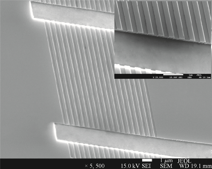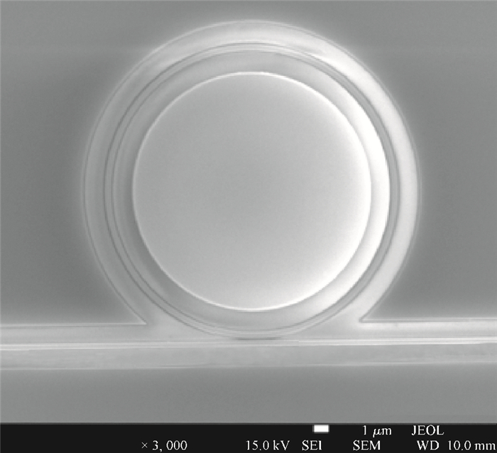
Fig. 1.
SEM photographs of the silicon MR resonator.
SEMICONDUCTOR INTEGRATED CIRCUITS
Xiaogang Tong, Jun Liu and Chenyang Xue
Corresponding author: Liu Jun, Email:liuj@nuc.edu.cn; Xue Chenyang, xuechenyang@nuc.edu.cn
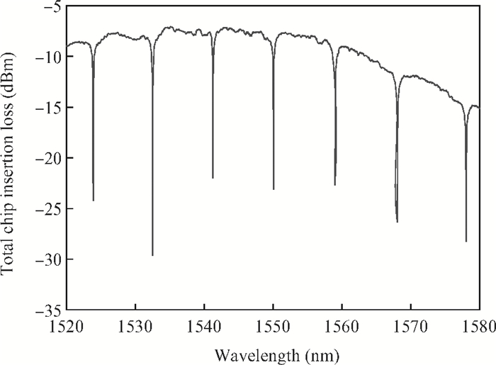
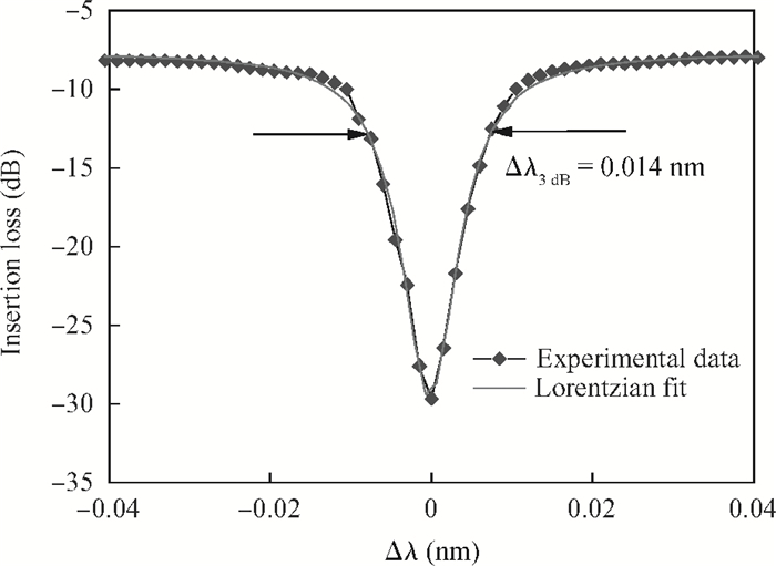
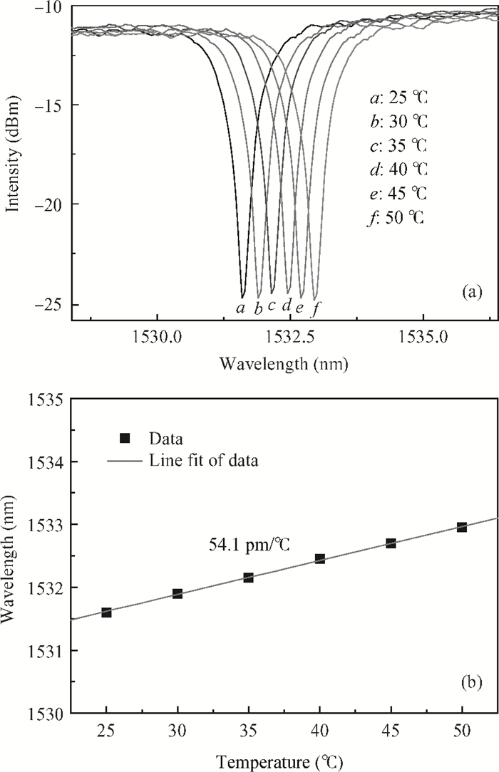
Abstract: An ultra-small integrated photonic circuit has been proposed, which incorporates a high-quality-factor passive micro-ring resonator (MR) linked to a vertical grating coupler on a standard silicon-on-insulator (SOI) substrate. The experimental results demonstrate that the MR propagation loss is 0.532 dB/cm with a 10 μm radius ring resonator, the intrinsic quality factor is as high as 202.000, the waveguide grating wavelength response curve is a 1 dB bandwidth of 40 nm at 1540 nm telecommunication wavelengths, and the measured fiber-to-fiber coupling loss is 10 dB. Furthermore, the resonator wavelength temperature dependence of the 450 nm wide micro-ring resonator is 54.1 pm/℃. Such vertical grating coupler and low loss MR-integrated components greatly promote a key element in biosensors and high-speed interconnect communication applications.
Keywords: high-quality-factor, passive micro-ring resonators, waveguide grating couplers, integrated photonic circuit
| [1] |
Zimmermann L, Tekin T, Schroeder H, et al. How to bring nanophotonics to application-silicon photonics packaging. LEOS Newsletter, 2008, 22:4 http://www.photonics.intec.ugent.be/download/pub_2811.pdf
|
| [2] |
Xu Q, Manipatruni S, Schmidt B, et al. 12.5 Gbit/s carrier-injection-based silicon micro-ring silicon modulators. Opt Express, 2007, 15:430 doi: 10.1364/OE.15.000430
|
| [3] |
Wu Zhigang, Zhang Weigang, Wang Zhi, et al. Fabrication and evaluation of Bragg gratings on optimally designed silicon-on-insulator rib waveguides using electron-beam lithography. Chinese Journal of Semiconductors, 2006, 27(8):1347 https://waseda.pure.elsevier.com/en/publications/fabrication-and-evaluation-of-bragg-gratings-on-optimally-designe
|
| [4] |
Li Shuai, Wu Yuanda, Yin Xiaojie, et al. Tunable filters based on an SOI nano-wire waveguide micro ring resonator. Journal of Semiconductors, 2011, 32(8):084007 doi: 10.1088/1674-4926/32/8/084007
|
| [5] |
Ren G H, Cheng S W, Cheng Y P, et al. Study on inverse taper based mode transformer for low loss coupling between silicon wire waveguide and lensed fiber. Opt Commun, 2011, 284:4782 doi: 10.1016/j.optcom.2011.05.072
|
| [6] |
Manolatou C, Lipson M. All-optical silicon modulators based on carrier injection by two-photon absorption. J Lightwave Technol, 2006, 24:1433 doi: 10.1109/JLT.2005.863326
|
| [7] |
Po D, Preble S F, Lipson M. All-optical compact silicon comb switch. Opt Express, 2007, 15:9600 doi: 10.1364/OE.15.009600
|
| [8] |
Little B E, Chu S T, Haus H A, et al. Microring resonator channel dropping filters. J Lightwave Technol, 1997, 15:998 doi: 10.1109/50.588673
|
| [9] |
Xu D X, Densmore A, Delâge A, et al. Folded cavity SOI microring sensors for high sensitivity and real time measurement of biomolecular binding. Opt Express, 2008, 16:15137 doi: 10.1364/OE.16.015137
|
| [10] |
Xia F N, Sekaric L, Vlasov Y. Ultracompact optical buffers on a silicon chip. Nat Photonics, 2007, 1:65 doi: 10.1038/nphoton.2006.42
|
| [11] |
Xu Q F, Dong P, Lipson M. Breaking the delay-bandwidth limit in a photonic structure. Nat Phys, 2007, 3:406 doi: 10.1038/nphys600
|
| [12] |
Xiao S, Khan M H, Shen H, et al. Modeling and measurement of losses in silicon-on-insulator resonators and bends. Opt Express, 2007, 15:10553 doi: 10.1364/OE.15.010553
|
| [13] |
Liu S W, Xiao M. Electro-optic switch in ferroelectric thin films mediated by surface plasmons. Appl Phys Lett, 2006, 88:14 http://www.uark.edu/misc/quantopt/apl143512.pdf
|
| [14] |
Luo L W, Wiederhecker G S, Cardenas J, et al. High quality factor etchless silicon photonic ring resonators. Opt Express, 2011, 19:6284 doi: 10.1364/OE.19.006284
|
| [15] |
Rabiei P, Steier W H, Zhang C, et al. Polymer micro-ring filters and modulators. J Lightwave Technol, 2002, 20:1968 doi: 10.1109/JLT.2002.803058
|
| [16] |
Kokubun Y, Yoneda S, Matsuura S. Temperature-independent optical filter at 1.55-μm wavelength using a silica-based thermal waveguide. Electron Lett, 1998, 34:367 doi: 10.1049/el:19980245
|


Article views: 4609 Times PDF downloads: 82 Times Cited by: 0 Times
Received: 29 September 2012 Revised: 05 March 2013 Online: Published: 01 August 2013
| Citation: |
Xiaogang Tong, Jun Liu, Chenyang Xue. High-Q micro-ring resonators and grating couplers for silicon-on-insulator integrated photonic circuits[J]. Journal of Semiconductors, 2013, 34(8): 085006. doi: 10.1088/1674-4926/34/8/085006
****
X G Tong, J Liu, C Y Xue. High-Q micro-ring resonators and grating couplers for silicon-on-insulator integrated photonic circuits[J]. J. Semicond., 2013, 34(8): 085006. doi: 10.1088/1674-4926/34/8/085006.

|
| [1] |
Zimmermann L, Tekin T, Schroeder H, et al. How to bring nanophotonics to application-silicon photonics packaging. LEOS Newsletter, 2008, 22:4 http://www.photonics.intec.ugent.be/download/pub_2811.pdf
|
| [2] |
Xu Q, Manipatruni S, Schmidt B, et al. 12.5 Gbit/s carrier-injection-based silicon micro-ring silicon modulators. Opt Express, 2007, 15:430 doi: 10.1364/OE.15.000430
|
| [3] |
Wu Zhigang, Zhang Weigang, Wang Zhi, et al. Fabrication and evaluation of Bragg gratings on optimally designed silicon-on-insulator rib waveguides using electron-beam lithography. Chinese Journal of Semiconductors, 2006, 27(8):1347 https://waseda.pure.elsevier.com/en/publications/fabrication-and-evaluation-of-bragg-gratings-on-optimally-designe
|
| [4] |
Li Shuai, Wu Yuanda, Yin Xiaojie, et al. Tunable filters based on an SOI nano-wire waveguide micro ring resonator. Journal of Semiconductors, 2011, 32(8):084007 doi: 10.1088/1674-4926/32/8/084007
|
| [5] |
Ren G H, Cheng S W, Cheng Y P, et al. Study on inverse taper based mode transformer for low loss coupling between silicon wire waveguide and lensed fiber. Opt Commun, 2011, 284:4782 doi: 10.1016/j.optcom.2011.05.072
|
| [6] |
Manolatou C, Lipson M. All-optical silicon modulators based on carrier injection by two-photon absorption. J Lightwave Technol, 2006, 24:1433 doi: 10.1109/JLT.2005.863326
|
| [7] |
Po D, Preble S F, Lipson M. All-optical compact silicon comb switch. Opt Express, 2007, 15:9600 doi: 10.1364/OE.15.009600
|
| [8] |
Little B E, Chu S T, Haus H A, et al. Microring resonator channel dropping filters. J Lightwave Technol, 1997, 15:998 doi: 10.1109/50.588673
|
| [9] |
Xu D X, Densmore A, Delâge A, et al. Folded cavity SOI microring sensors for high sensitivity and real time measurement of biomolecular binding. Opt Express, 2008, 16:15137 doi: 10.1364/OE.16.015137
|
| [10] |
Xia F N, Sekaric L, Vlasov Y. Ultracompact optical buffers on a silicon chip. Nat Photonics, 2007, 1:65 doi: 10.1038/nphoton.2006.42
|
| [11] |
Xu Q F, Dong P, Lipson M. Breaking the delay-bandwidth limit in a photonic structure. Nat Phys, 2007, 3:406 doi: 10.1038/nphys600
|
| [12] |
Xiao S, Khan M H, Shen H, et al. Modeling and measurement of losses in silicon-on-insulator resonators and bends. Opt Express, 2007, 15:10553 doi: 10.1364/OE.15.010553
|
| [13] |
Liu S W, Xiao M. Electro-optic switch in ferroelectric thin films mediated by surface plasmons. Appl Phys Lett, 2006, 88:14 http://www.uark.edu/misc/quantopt/apl143512.pdf
|
| [14] |
Luo L W, Wiederhecker G S, Cardenas J, et al. High quality factor etchless silicon photonic ring resonators. Opt Express, 2011, 19:6284 doi: 10.1364/OE.19.006284
|
| [15] |
Rabiei P, Steier W H, Zhang C, et al. Polymer micro-ring filters and modulators. J Lightwave Technol, 2002, 20:1968 doi: 10.1109/JLT.2002.803058
|
| [16] |
Kokubun Y, Yoneda S, Matsuura S. Temperature-independent optical filter at 1.55-μm wavelength using a silica-based thermal waveguide. Electron Lett, 1998, 34:367 doi: 10.1049/el:19980245
|

 WeChat ID
Journal of Semiconductors © 2017 All Rights Reserved 京ICP备05085259号-2

 DownLoad: