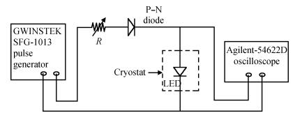
Fig. 1.
Schematic diagram of the experimental set up used for the OCVD LED measurement.
SEMICONDUCTOR PHYSICS
P. Dalapati, N. B. Manik and A. N. Basu
Corresponding author: N. B. Manik, Email:nb_manik@yahoo.co.in
Abstract: The influence of temperature on the intensity of light emitted by as well as the carrier life time τ of a standard AlGaAs based light emitting diode has been investigated in the temperature range from 345 to 136 K. The open-circuit voltage decay (OCVD) technique has been used for measured the carrier lifetime. Our experimental results reveal a 16% average increase in intensity and a 163.482-19.765 ns variation in carrier lifetime in the above temperature range. Further, theoretical and experimental analysis show that for negligible carrier density the intensity is inversely proportional to carrier lifetime for this sample.
Keywords: LED, low temperature, intensity, ideality factor, carrier lifetime
| [1] |
Lee Y J, Lee C J, Chen C H. Determination of junction temperature in InGaN and AlGaInP light-emitting diodes. IEEE J Quantum Electron, 2010, 46:1450 doi: 10.1109/JQE.2010.2050866
|
| [2] |
Manik N B, Basu A N, Mukherjee S C. Characterisation of the photodetector and light emitting diode at above liquid nitrogen temperature. Cryogenics, 2000, 40:341 doi: 10.1016/S0011-2275(00)00036-9
|
| [3] |
Guo Weling, Jia Xuejiao, Yin Fei, et al. Characteristics of high power LEDs at high and low temperature. Journal of Semiconductors, 2011, 32:4007
|
| [4] |
Vanderdoes Debye J A W, Blow L. Room temperature minority carrier life time and efficiency of p-type GaAs1-xPx. Journal of Luminescence, 1976, 14:101 https://es.scribd.com/document/269892788/Advanced-Biomedical-Engineering
|
| [5] |
Vitezslav B, Zdenek N. OCVD carrier life time measurements on an inhomogeneousdiode structure. SER Elec Energ, 2002, 15:33 http://technav.ieee.org/tag/8731/silicon-devices
|
| [6] |
Bhattacharya D K, Abhai M. Determination of recombination center position from the temperature dependence of minority car-rier lifetime in the base region of p-n junction solar cells. J Appl Phys, 1985, 57:2942 doi: 10.1063/1.335234
|
| [7] |
Mathur P C, Sharma R P, Saxena P, et al. Temperature dependence of minority carrier lifetime in single-crystal and polycrystalline Si solar cells. J Appl Phys, 1981, 52:3651 doi: 10.1063/1.329101
|
| [8] |
Mahan J E, Ekstedt T W, Frank R I. Measurement of minority carrier lifetime in solar cells from photo-induced open-circuit voltage decay. IEEE Trans Electron Devices, 1979, 26:733 doi: 10.1109/T-ED.1979.19487
|
| [9] |
Vishnoi A, Gopal R, Dwivedi R, et al. Measurement of minority carrier lifetime of solar cells using surface voltage and current transients. Solid-Stare Electron, 1990, 33:41l https://arxiv.org/pdf/1511.07887.pdf
|
| [10] |
Milan T, Jaroslav P, Andrej V, et al. Application of open circuit voltage decay to the characterization of epitaxial layer. Electrical Eng, 2004, 55:239
|
| [11] |
Sertap K A, Nese K, Sener O. The circuit point of view of the temperature dependent open circuit voltage decay of the solar cell. Solar Energy, 2009, 83:1446 doi: 10.1016/j.solener.2009.03.009
|
| [12] |
Vobecky J, Hazdra P, Zahlava V. Open circuit voltage decay lifetime of ion irradiated devices. Microelectron J, 1999, 30:513 doi: 10.1016/S0026-2692(98)00173-6
|
| [13] |
Pisarkiewicz T. Photodecay method in investigation of materials and photovoltaic structures. Opto-Electron Rev, 2004, 12:33 https://tw.arxiv.org/pdf/1706.02397
|
| [14] |
Salach-Bielecki R, Pisarkiewicz T, Stapinski T, et al. Influence of junction parameters on the open circuit voltage decay in solar cells. Opto-Electron Rev, 2004, 12:79
|
| [15] |
Tseng K J, Pan S. Modified charge-control equation for simulation of diode reverse recovery. Electron Lett, 1996, 32:404 doi: 10.1049/el:19960210
|
| [16] |
Ravinandan M, Koteswara R P, Rajagopal R V. Temperature dependence of current-voltage (Ⅰ-Ⅴ) characteristics of Pt/Au Schottky contacts on n-type GaN. J Optoelectron Adv Mater, 2008, 10:2787 http://wulixb.iphy.ac.cn/EN/volumn/volumn_522.shtml
|
| [17] |
Tunc T, Dokme I, Altindal S, et al. Temperature dependent current-voltage (Ⅰ-Ⅴ) characteristics of Au/n-Si (111) Schottky barrier diodes (SBDs) with polyvinyl alcohol (Co, Ni-doped) interfacial layer. Optoelectron Adv Mater, 2010, 4:947
|
| [18] |
Singh R, Arora S K, Renu T, et al. Temperature dependence of current-voltage characteristics of Au/n-GaAs epitaxial Schottky diode. Bull Mater Sci, 2000, 23:471 doi: 10.1007/BF02903886
|
| [19] |
Zhu Shiyang, Ru Guoping, Qu Xinping, et al. Double threshold behaviour of Ⅰ-Ⅴ characteristics of CoSi2/Si Schottky contacts. Chin Phys B, 2002, 11:156 doi: 10.1088/1009-1963/11/2/310
|
| [20] |
Acharya Y B, Vyavahare P D. Temperature characteristics of the device constant (n) of a light emitting diode. Solid-State Electron, 1999, 43:645 doi: 10.1016/S0038-1101(98)00291-3
|
| [21] |
Bergman J P, Hallin C, Janzen E. Temperature dependence of the minority carrier, lifetime in GaAs/AlGaAs double heterostructures. J Appl Phys, 1995, 78:4808 doi: 10.1063/1.360740
|
| [22] |
http: //www. ioffe. ru/SVA/NSM/Semicond/AlGaAs/bandstr. html
|
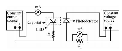
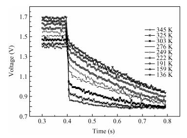
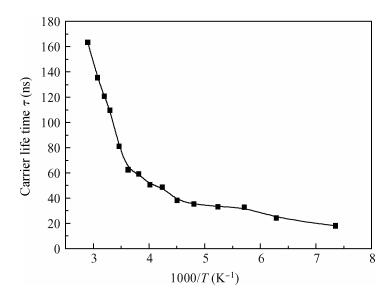
Table 1.
Variation of carrier lifetime

|
| [1] |
Lee Y J, Lee C J, Chen C H. Determination of junction temperature in InGaN and AlGaInP light-emitting diodes. IEEE J Quantum Electron, 2010, 46:1450 doi: 10.1109/JQE.2010.2050866
|
| [2] |
Manik N B, Basu A N, Mukherjee S C. Characterisation of the photodetector and light emitting diode at above liquid nitrogen temperature. Cryogenics, 2000, 40:341 doi: 10.1016/S0011-2275(00)00036-9
|
| [3] |
Guo Weling, Jia Xuejiao, Yin Fei, et al. Characteristics of high power LEDs at high and low temperature. Journal of Semiconductors, 2011, 32:4007
|
| [4] |
Vanderdoes Debye J A W, Blow L. Room temperature minority carrier life time and efficiency of p-type GaAs1-xPx. Journal of Luminescence, 1976, 14:101 https://es.scribd.com/document/269892788/Advanced-Biomedical-Engineering
|
| [5] |
Vitezslav B, Zdenek N. OCVD carrier life time measurements on an inhomogeneousdiode structure. SER Elec Energ, 2002, 15:33 http://technav.ieee.org/tag/8731/silicon-devices
|
| [6] |
Bhattacharya D K, Abhai M. Determination of recombination center position from the temperature dependence of minority car-rier lifetime in the base region of p-n junction solar cells. J Appl Phys, 1985, 57:2942 doi: 10.1063/1.335234
|
| [7] |
Mathur P C, Sharma R P, Saxena P, et al. Temperature dependence of minority carrier lifetime in single-crystal and polycrystalline Si solar cells. J Appl Phys, 1981, 52:3651 doi: 10.1063/1.329101
|
| [8] |
Mahan J E, Ekstedt T W, Frank R I. Measurement of minority carrier lifetime in solar cells from photo-induced open-circuit voltage decay. IEEE Trans Electron Devices, 1979, 26:733 doi: 10.1109/T-ED.1979.19487
|
| [9] |
Vishnoi A, Gopal R, Dwivedi R, et al. Measurement of minority carrier lifetime of solar cells using surface voltage and current transients. Solid-Stare Electron, 1990, 33:41l https://arxiv.org/pdf/1511.07887.pdf
|
| [10] |
Milan T, Jaroslav P, Andrej V, et al. Application of open circuit voltage decay to the characterization of epitaxial layer. Electrical Eng, 2004, 55:239
|
| [11] |
Sertap K A, Nese K, Sener O. The circuit point of view of the temperature dependent open circuit voltage decay of the solar cell. Solar Energy, 2009, 83:1446 doi: 10.1016/j.solener.2009.03.009
|
| [12] |
Vobecky J, Hazdra P, Zahlava V. Open circuit voltage decay lifetime of ion irradiated devices. Microelectron J, 1999, 30:513 doi: 10.1016/S0026-2692(98)00173-6
|
| [13] |
Pisarkiewicz T. Photodecay method in investigation of materials and photovoltaic structures. Opto-Electron Rev, 2004, 12:33 https://tw.arxiv.org/pdf/1706.02397
|
| [14] |
Salach-Bielecki R, Pisarkiewicz T, Stapinski T, et al. Influence of junction parameters on the open circuit voltage decay in solar cells. Opto-Electron Rev, 2004, 12:79
|
| [15] |
Tseng K J, Pan S. Modified charge-control equation for simulation of diode reverse recovery. Electron Lett, 1996, 32:404 doi: 10.1049/el:19960210
|
| [16] |
Ravinandan M, Koteswara R P, Rajagopal R V. Temperature dependence of current-voltage (Ⅰ-Ⅴ) characteristics of Pt/Au Schottky contacts on n-type GaN. J Optoelectron Adv Mater, 2008, 10:2787 http://wulixb.iphy.ac.cn/EN/volumn/volumn_522.shtml
|
| [17] |
Tunc T, Dokme I, Altindal S, et al. Temperature dependent current-voltage (Ⅰ-Ⅴ) characteristics of Au/n-Si (111) Schottky barrier diodes (SBDs) with polyvinyl alcohol (Co, Ni-doped) interfacial layer. Optoelectron Adv Mater, 2010, 4:947
|
| [18] |
Singh R, Arora S K, Renu T, et al. Temperature dependence of current-voltage characteristics of Au/n-GaAs epitaxial Schottky diode. Bull Mater Sci, 2000, 23:471 doi: 10.1007/BF02903886
|
| [19] |
Zhu Shiyang, Ru Guoping, Qu Xinping, et al. Double threshold behaviour of Ⅰ-Ⅴ characteristics of CoSi2/Si Schottky contacts. Chin Phys B, 2002, 11:156 doi: 10.1088/1009-1963/11/2/310
|
| [20] |
Acharya Y B, Vyavahare P D. Temperature characteristics of the device constant (n) of a light emitting diode. Solid-State Electron, 1999, 43:645 doi: 10.1016/S0038-1101(98)00291-3
|
| [21] |
Bergman J P, Hallin C, Janzen E. Temperature dependence of the minority carrier, lifetime in GaAs/AlGaAs double heterostructures. J Appl Phys, 1995, 78:4808 doi: 10.1063/1.360740
|
| [22] |
http: //www. ioffe. ru/SVA/NSM/Semicond/AlGaAs/bandstr. html
|


Article views: 4443 Times PDF downloads: 78 Times Cited by: 0 Times
Received: 02 February 2013 Revised: Online: Published: 01 September 2013
| Citation: |
P. Dalapati, N. B. Manik, A. N. Basu. Effect of temperature on the intensity and carrier lifetime of an AlGaAs based red light emitting diode[J]. Journal of Semiconductors, 2013, 34(9): 092001. doi: 10.1088/1674-4926/34/9/092001
****
P. Dalapati, N. B. Manik, A. N. Basu. Effect of temperature on the intensity and carrier lifetime of an AlGaAs based red light emitting diode[J]. J. Semicond., 2013, 34(9): 092001. doi: 10.1088/1674-4926/34/9/092001.

|
| [1] |
Lee Y J, Lee C J, Chen C H. Determination of junction temperature in InGaN and AlGaInP light-emitting diodes. IEEE J Quantum Electron, 2010, 46:1450 doi: 10.1109/JQE.2010.2050866
|
| [2] |
Manik N B, Basu A N, Mukherjee S C. Characterisation of the photodetector and light emitting diode at above liquid nitrogen temperature. Cryogenics, 2000, 40:341 doi: 10.1016/S0011-2275(00)00036-9
|
| [3] |
Guo Weling, Jia Xuejiao, Yin Fei, et al. Characteristics of high power LEDs at high and low temperature. Journal of Semiconductors, 2011, 32:4007
|
| [4] |
Vanderdoes Debye J A W, Blow L. Room temperature minority carrier life time and efficiency of p-type GaAs1-xPx. Journal of Luminescence, 1976, 14:101 https://es.scribd.com/document/269892788/Advanced-Biomedical-Engineering
|
| [5] |
Vitezslav B, Zdenek N. OCVD carrier life time measurements on an inhomogeneousdiode structure. SER Elec Energ, 2002, 15:33 http://technav.ieee.org/tag/8731/silicon-devices
|
| [6] |
Bhattacharya D K, Abhai M. Determination of recombination center position from the temperature dependence of minority car-rier lifetime in the base region of p-n junction solar cells. J Appl Phys, 1985, 57:2942 doi: 10.1063/1.335234
|
| [7] |
Mathur P C, Sharma R P, Saxena P, et al. Temperature dependence of minority carrier lifetime in single-crystal and polycrystalline Si solar cells. J Appl Phys, 1981, 52:3651 doi: 10.1063/1.329101
|
| [8] |
Mahan J E, Ekstedt T W, Frank R I. Measurement of minority carrier lifetime in solar cells from photo-induced open-circuit voltage decay. IEEE Trans Electron Devices, 1979, 26:733 doi: 10.1109/T-ED.1979.19487
|
| [9] |
Vishnoi A, Gopal R, Dwivedi R, et al. Measurement of minority carrier lifetime of solar cells using surface voltage and current transients. Solid-Stare Electron, 1990, 33:41l https://arxiv.org/pdf/1511.07887.pdf
|
| [10] |
Milan T, Jaroslav P, Andrej V, et al. Application of open circuit voltage decay to the characterization of epitaxial layer. Electrical Eng, 2004, 55:239
|
| [11] |
Sertap K A, Nese K, Sener O. The circuit point of view of the temperature dependent open circuit voltage decay of the solar cell. Solar Energy, 2009, 83:1446 doi: 10.1016/j.solener.2009.03.009
|
| [12] |
Vobecky J, Hazdra P, Zahlava V. Open circuit voltage decay lifetime of ion irradiated devices. Microelectron J, 1999, 30:513 doi: 10.1016/S0026-2692(98)00173-6
|
| [13] |
Pisarkiewicz T. Photodecay method in investigation of materials and photovoltaic structures. Opto-Electron Rev, 2004, 12:33 https://tw.arxiv.org/pdf/1706.02397
|
| [14] |
Salach-Bielecki R, Pisarkiewicz T, Stapinski T, et al. Influence of junction parameters on the open circuit voltage decay in solar cells. Opto-Electron Rev, 2004, 12:79
|
| [15] |
Tseng K J, Pan S. Modified charge-control equation for simulation of diode reverse recovery. Electron Lett, 1996, 32:404 doi: 10.1049/el:19960210
|
| [16] |
Ravinandan M, Koteswara R P, Rajagopal R V. Temperature dependence of current-voltage (Ⅰ-Ⅴ) characteristics of Pt/Au Schottky contacts on n-type GaN. J Optoelectron Adv Mater, 2008, 10:2787 http://wulixb.iphy.ac.cn/EN/volumn/volumn_522.shtml
|
| [17] |
Tunc T, Dokme I, Altindal S, et al. Temperature dependent current-voltage (Ⅰ-Ⅴ) characteristics of Au/n-Si (111) Schottky barrier diodes (SBDs) with polyvinyl alcohol (Co, Ni-doped) interfacial layer. Optoelectron Adv Mater, 2010, 4:947
|
| [18] |
Singh R, Arora S K, Renu T, et al. Temperature dependence of current-voltage characteristics of Au/n-GaAs epitaxial Schottky diode. Bull Mater Sci, 2000, 23:471 doi: 10.1007/BF02903886
|
| [19] |
Zhu Shiyang, Ru Guoping, Qu Xinping, et al. Double threshold behaviour of Ⅰ-Ⅴ characteristics of CoSi2/Si Schottky contacts. Chin Phys B, 2002, 11:156 doi: 10.1088/1009-1963/11/2/310
|
| [20] |
Acharya Y B, Vyavahare P D. Temperature characteristics of the device constant (n) of a light emitting diode. Solid-State Electron, 1999, 43:645 doi: 10.1016/S0038-1101(98)00291-3
|
| [21] |
Bergman J P, Hallin C, Janzen E. Temperature dependence of the minority carrier, lifetime in GaAs/AlGaAs double heterostructures. J Appl Phys, 1995, 78:4808 doi: 10.1063/1.360740
|
| [22] |
http: //www. ioffe. ru/SVA/NSM/Semicond/AlGaAs/bandstr. html
|

 WeChat ID
Journal of Semiconductors © 2017 All Rights Reserved 京ICP备05085259号-2

 DownLoad: