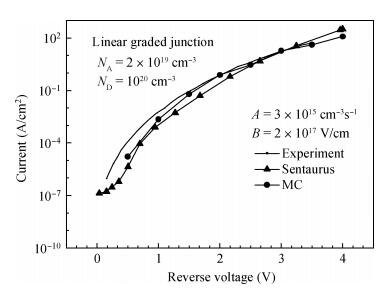
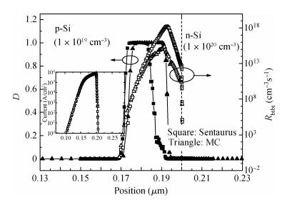
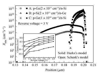
Processing math: 100%
J. Semicond. > 2013, Volume 34 > Issue 9 > 092002

SEMICONDUCTOR PHYSICS

Comparison of band-to-band tunneling models in Si and Si-Ge junctions

Yipeng Jiao1, Kangliang Wei2, Taihuan Wang1, Gang Du2 and Xiaoyan Liu2,

+ Author Affiliations

 Corresponding author: Liu Xiaoyan, Email:xyliu@ime.pku.edu.cn

DOI: 10.1088/1674-4926/34/9/092002

PDF

Abstract: We compared several different band-to-band tunneling (BTBT) models with both Sentaurus and the two-dimensional full-band Monte Carlo simulator in Si homo-junctions and Si-Ge hetero-junctions. It was shown that in Si homo-junctions, different models could achieve similar results. However, in the Si-Ge hetero-junctions, there were significant differences among these models at high reverse biases (over 2 V). Compared to the nonlocal model, the local models in Sentaurus underrated the BTBT rate distinctly, and the Monte Carlo method was shown to give a better approximation. Additionally, it was found that in the Si region near the interface of the Si-Ge hetero-junctions, the direct tunneling rates increased largely due to the interaction of the band structures of Si and Ge.

Key words: hetero-structureMonte Carlo device simulationcarrier transportband-to-band tunneling

Much work has been done on the mechanism of band-to-band tunneling (BTBT), which is the basic principle for tunneling field effect transistors (TFET), especially in indirect semiconductors[1-4], such as Si and Ge. However, because the L and Γ valleys of the conduction band have small energy differences (0.14 eV) in Ge, direct tunneling dominates the total tunneling process[5, 6]. While in Si, the situation is just the opposite due to a larger difference, 2.3 eV, between the main valley and sub-valley. What's more, the BTBT mechanism becomes more complex in Si–Ge hetero-structures, which are regarded as one of the most important methods to optimize TFET[7]. Hence, the accuracy of BTBT models in Si–Ge hetero-junctions is critical to investigate the performance of these devices. However, few works so far have discussed this issue[8, 9].

In this paper, we will mainly focus on the comparison among three widely-used BTBT models when they are employed in Si homo-junction and Si–Ge hetero-junction simulation at reverse biases. At the same time, the performance of our recently developed two-dimensional (2D) full-band Monte Carlo (FBMC) simulator with BTBT models is also evaluated (by comparison with Sentaurus). This FBMC simulator is then used to study the BTBT mechanism in Si–Ge hetero-junctions with diverse doping concentrations.

There are three BTBT tunneling models that can be chosen in Sentaurus: Hurkx's model, Schenk's model and the nonlocal path model.

The most widely used, Hurkx's model, gives[10, 11],

RBTBT=ADεpeB/ε.

(1)

This model is based on a two-band model. RBTBT is the BTBT rate and A and B are parameters, which will be discussed in detail below. ε is the local electric field. For the direct tunneling process, P= 2, and for the phonon-assisted tunneling process, P= 2.5. D, called the net generation factor, can be calculated from,

D=npn2i,,eff(n+ni,,eff)(p+ni,,eff).

(2)

The effect of D will be discussed in Section 4.

In the device with a steep p–n junction and high field, exceeding (approximately) 8 × 10⁵ V/cm, Schenk's model[12] is used to compute the phonon-assisted BTBT rate,

RBTBT=ASDε[(FC)3/2exp(FCε)exphωkt1+,(FC)3/2exp(FCε)1exphωkt],

(3)

with

F±C=expBS(Eg±hω)3/2.

(4)

The upper sign refers to the generation process (np <, n2i,,eff) and the lower sign refers to the recombination process (np > n2i,,eff). hω is the energy of the transverse acoustic phonon, about 19 meV in Si (ΓX) and 8.6 meV in Ge (both ΓX and ΓL)[13], and ε is the local electric field. As and Bs are parameters, which are 8.977 × 1020 cm1s1V2 and 2.14667 × 10⁷ Vcm1eV3/2, respectively[12].

For a more accurate calculation, the nonlocal BTBT models in the Sentaurus TCAD should be switched on in the device simulation. This model allows the simulator to dynamically search for the tunneling path that has a direction which is opposite to the gradient of the valence band. To compute the BTBT rate of such a method is very complex and the method has been discussed in Ref.[14], but in the uniform electric-field limit and one-dimensional case, these equations can be reduced to a form the same as Eq. (1)[15].

For both Si and Ge, the values of A,B and P for Eq. (1) have been listed in Table 1.

Table  1.  The values of parameters A, B and P with tunneling directions along [100] in Eq. (1). The "Direct BTBT" and "Indirect BTBT" columns list the results calculated in Ref. [14], and the "Sentaurus" columns list the default values in Sentaurus[16].
DownLoad: CSV  | Show Table

For Si, where the indirect transitions are dominant in the BTBT process, the theoretical values of A and B are 3.29 × 1015 cm3s1 and 2.38 × 10⁷ V/cm from Table 1. While from the experimental data[17], parameter A varies between 2 × 10¹⁵ and 3 × 1015 cm3s1, and B is approximately 2.0 × 10⁷ V/cm. Therefore, in this paper, the values of parameters A and B for Si are finally chosen as 3.0 × 1015 cm3s1 and 2.0 × 10⁷ V/cm, respectively, reproducing the experimental data in Ref. [10] very well (Fig. 1).

Figure  1.  Simulated BTBT current density of an Si linearly graded junction compared with the experimental data.

The 2D FBMC simulator has been discussed in detail in Refs. [18, 19]. The band structures, including four conductions bands and three valence bands, were calculated from the local empirical pseudo-potential method. Scattering mechanisms, including acoustic and optical phonon scattering, and impact ionization scattering for both Ge and Si were considered.

The non-self-consistent mode was used in our Monte Carlo (MC) simulator as follows. Firstly, we obtained the electrostatic potential for the whole device using the drift–diffusion method, and then this potential was kept frozen during the simulation. For each step, the program calculated the BTBT generation or recombination rate over the whole device using Eq. (1) or Eq. (3), and the generated particles with charge Pc, by

Pc=RBTBTΔSΔt,

(5)

where RBTBT is the rate of, BTBT generation and recombination, and ΔS is the area of the mesh[9].

As a comparison with the MC method, in Sentaurus we used the Fermi-Dirac statistics model (Fermi), the drift-diffusion carrier transport model, the doping–dependent mobility model (DopingDep), and the high-field velocity saturation model (HighField saturation). The doping-dependent band-gap-narrowing model (BandGap narrowing) was also switched on.

In order to verify the validity of the MC simulator, the results of an Si diode at a series of forward biases (0.15–1 V) were obtained (Fig. 2). At a forward bias, BTBT can hardly occur since the conduction band edge is located above the valence band edge (see the inset of Fig. 2). It is found that the forward currents computed by the two simulators agree well with each other when the reverse bias is above 0.5 V. That is to say, there is no difference between the results calculated from them if BTBT does not occur. These results prove the reliability of our MC simulator, as well as the reasonability of the comparisons in this paper.

Figure  2.  Simulation results for the Si step homo-junction by Sentaurus and the MC simulators at forward bias. The valence and conduction band at 0.5 V is shown in the inset.

Figure 3 plots the BTBT currents of an Si homo-junction at various reverse biases, from 1 to 4 V. It is worth noting that the current density obtained from Schenk's model is one order of magnitude less than that from Hurkx's model in both Sentaurus and the MC simulator in the range 1.5–4 V (reverse bias). This can also be verified from the difference of RBTBT between the two models (Fig. 4). In addition, although the dynamic nonlocal path BTBT model demonstrates a wider spatial range of generation and recombination rate in the device, the currents are almost the same as the values calculated from Hurkx's model in an Si homo-junction.

Figure  3.  Simulated BTBT current density of an Si homo-junction with three BTBT models in Sentaurus and the MC simulator. The solid line plots the results in Ref. [10].
Figure  4.  Simulated BTBT rate of an Si homo-junction with two models at different biases.

On the other hand, at very low reverse biases (0–1.5 V), the current obtained from the MC simulator is much smaller than that from Sentaurus. In Fig. 5, it is found that at the peak of the BTBT rates, D drops to very low values in the MC simulator, while it is still maintained at about 1 (which means that there is no attenuation for Rbtbt) at the same position in Sentaurus. Because D has a close relationship with the carrier density (Eq. (2)), it is obvious that the carrier density in the MC method does not reach the expected value at a low reverse bias due to this method's drawback in addressing a retarding field, resulting in a relatively low BTBT current.

Figure  5.  The D factor (right vertical axis) and BTBT (left vertical axis) rates calculated by Hurkx's model at 1 V (reverse bias). The curves with square symbols are the results from Sentaurus, and the curves with triangular symbols are from the MC simulator. The inset shows the electrostatic fields from the two simulators.

However, in the Si–Ge hetero-structure, the situation is very different. The IV characteristics of two step diodes (Si and Si–Ge) are shown in Fig. 6, and they have the same doping concentrations. With both models (Hurkx and Schenk), the currents in the Si–Ge hetero-junctions are larger than the ones in the Si homo-junctions. Figure 7 gives a detailed comparison of the currents calculated with different BTBT models in an Si–Ge diode. It should be noted that in order to have a full understanding of these models, we also introduced the direct and indirect BTBT parameters listed above to our MC simulator, but they are still treated as local models. Obviously, in a local BTBT model of Sentaurus (Hurkx's model), the current increases rapidly at a low voltage and then tends to be saturated. The nonlocal model gives a larger current value than the local one at the same bias, especially when the voltage comes to more than 1 V (reverse bias), in agreement with the BTBT rates in Fig. 8. However, the results of the MC method are more sophisticated. At low reverse voltages, from 1 to 2 V, the current calculated from the MC method is very close to that from the local Hurkx's model, and this is because the model applied in our MC simulator is also a local one. However, when the reverse bias exceeds 2 V, the current increases rapidly in exponential form. It is noteworthy in Fig. 8(a) that from 0.10 μm to 0.13 μm, the BTBT rates using the MC method are larger than the corresponding values by Sentaurus at a reverse bias of 4 V. Hence, this implies that at a high reverse voltage (more than 3 V from Fig. 7), the local model in Sentaurus underestimates the spatial range and values of BTBT in the Si–Ge hetero-junctions, and the MC method can give current values very close to the ones with the nonlocal models, although this is very time-consuming. Additionally, for Sentaurus, in a hetero-junction it is sometimes very difficult to obtain convergence results if the nonlocal models are switched on. Hence, in order to get a suitable result, one must weigh the pros and cons of the different methods.

Figure  6.  Comparison of the current density of Si and Si–Ge diodes with two different BTBT models.
Figure  7.  Simulation results using different methods and BTBT models.
Figure  8.  The BTBT rates of the Si–Ge hetero-junction calculated under reverse biases of 1 V and 4 V.

For Ge devices, it has been reported that the direct BTBT process dominates over the indirect BTBT process[6, 14]. Similarly, in the Si–Ge hetero-junction used in Fig. 7, the direct tunneling current is about four orders of magnitude larger than the indirect one at the same bias, which is attributed to the band structures of Ge. Figure 9 is a comparison of RBTBT in three different Si–Ge diodes (A, B and C) using both Hurkx's and Schenk's models by the MC method at a reverse bias of 3 V, where this method is regarded to make a more accurate prediction for the BTBT current than the local models in Sentaurus and have a better convergence than the nonlocal models, according to the discussions above. The parameters in our MC simulator are the same as the default values in Sentaurus, and the doping of n-regions for all three devices is 1020 cm3. The BTBT rate calculated from Hurkx's model can be regarded as the total BTBT rate[14]. From diodes A and C, we find that the doping concentration has little effect on the BTBT rate differences of the two models, which seems to be an intrinsic property of the materials. This can also be verified by the comparisons between diodes A and B, which have the same doping profiles but different material composition. In diode A, where the depletion region mainly lies in the Ge region, the indirect BTBT rate has a smaller percentage than the direct one, while in diode B, the situation is just the opposite–-indirect transition takes a larger proportion. The BTBT rate curves of diode B also demonstrate that direct tunneling increases significantly at the Si region near the interface of the hetero-junction. This phenomenon is due to the electron in the valance band edge of Si being able to tunnel into the Γ valley in the conduction band of Ge near the interface, which is obviously direct tunneling.

Figure  9.  Simulated BTBT rates of three different hetero-structure diodes. The donor concentration of the n-region for each diode is 1020 cm3. The inset shows the IV curves from 1 to 4 V (reverse bias).

In this paper, we compared three different BTBT models with both a Sentaurus TCAD and 2D FBMC hetero-junction simulator in diverse Si homo-junctions and Si–Ge hetero-junctions. It was shown that in Si homo-junctions, these models achieved the same results in predicting the BTBT rates and currents at reverse biases. However, for the Si–Ge hetero-junctions, there were some contradictions in these models, especially at high reverse biases, and an underestimation of the tunneling rates and spatial range by local models could be seen from our comparisons.

It was also found that our improved MC simulator with BTBT models has good computation accuracy compared with Sentaurus, as well as good convergence for the hetero-junctions. In addition, we utilized our MC simulator to invest the BTBT phenomenon in three different abrupt Si–Ge hetero-junctions, and interactions of the direct and indirect transitions near the interface of the Si and Ge regions were observed for the first time.


[1]
Vandenberghe W, Sorée B, Magnus W, et al. Generalized phonon-assisted Zener tunneling in indirect semiconductors with non-uniform electric fields:a rigorous approach. J Appl Phys, 2011, 109(12):124503 doi: 10.1063/1.3595672
[2]
Kim S H, Kam H, Hu C, et al. Germanium-source tunnel field effect transistors with record high ION/IOFF. IEEE Symposium on VLSI Technology (VLSIT), 2009:178 http://ieeexplore.ieee.org/document/5200679/
[3]
Luisier M, Klimeck G. Performance comparisons of tunneling field effect transistors made of InSb, Carbon, and GaSb-InAs broken gap hetero-structures. IEEE International Electron Devices Meeting (IEDM), 2009:1 doi: 10.1007%2Fs00339-016-0151-3.pdf
[4]
Avci U E, Rios R, Kuhn K, et al. Comparison of performance, switching energy and process variations for the TFET and MOSFET in logic. IEEE Symposium on VLSI Technology (VLSIT), 2011:124 doi: 10.1007/978-3-319-31653-6_4/fulltext.html
[5]
Krishnamohan T, Kim D, Raghunathan S, et al. Double-gate strained-Ge hetero-structure tunneling FET (TFET) with record high drive currents and <<ll 60 mV/dec sub threshold slope. IEEE International Electron Devices Meeting (IEDM), 2008:1
[6]
Chynoweth A G, Feldmann W L, Lee C A, et al. Internal field emission at narrow silicon and germanium pn junctions. Phys Rev, 1960, 118(2):425 doi: 10.1103/PhysRev.118.425
[7]
Ionescu A M, Riel H. Tunnel field-effect transistors as energy-efficient electronic switches. Nature, 2011, 479(7373):329 doi: 10.1038/nature10679
[8]
Wei K L, Zeng L, Wang J C, et al. Simulation of band-to-band tunneling in Si/Ge and Si/Si1-xGex hetero-junctions by using Monte Carlo method. IEEE International Conference on Solid-State and Integrated Circuit Technology (ICSICT), 2012:1
[9]
Xia Z L, Du G, Song Y C, et al. Monte Carlo simulation of band-to-band tunneling in silicon devices. Jpn J Appl Phys, 2007, 46:2023 doi: 10.1143/JJAP.46.2023
[10]
Hurkx G A M, Klaassen D B M, Knuvers M P G. A new recombination model for device simulation including tunneling. IEEE Trans Electron Devices, 1992, 39(2):331 doi: 10.1109/16.121690
[11]
Liou J J. Modeling the tunneling current in reverse-biased p/n junctions. Solid-State Electron, 1990, 33(7):971 doi: 10.1016/0038-1101(90)90081-O
[12]
Schenk A. Rigorous theory and simplified model of the band-to-band tunneling in silicon. Solid-State Electron, 1993, 36(1):19 doi: 10.1016/0038-1101(93)90065-X
[13]
Fischetti M V, O'Regan T P, Narayanan S, et al. Theoretical study of some physical aspects of electronic transport in nMOSFETs at the 10-nm gate-length. IEEE Trans Electron Devices, 2007, 54(9):2116 doi: 10.1109/TED.2007.902722
[14]
Kao K H, Verhulst A S, Vandenberghe W G, et al. Direct and indirect band-to-band tunneling in germanium-based TFETs. IEEE Trans Electron Devices, 2012, 59(2):292 doi: 10.1109/TED.2011.2175228
[15]
Kane E O. Theory of tunneling. J Appl Phys, 1961, 32(1):83 doi: 10.1063/1.1735965
[16]
Sentaurus Device, Synopsys, Version D-2010. 03: 362
[17]
Wernersson L E, Kabeer S, Zela V, et al. SiGe Esaki tunnel diodes fabricated by UHV-CVD growth and proximity rapid thermal diffusion. Electron Lett, 2004, 40(1):83 doi: 10.1049/el:20040048
[18]
Wei K L, Liu X Y, Du G, et al. Simulation of carrier transport in hetero-structures using the 2D self-consistent full-band ensemble Monte Carlo method. Journal of Semiconductors, 2010, 31(8):084004 doi: 10.1088/1674-4926/31/8/084004
[19]
Du G, Liu X Y, Xia Z L, et al. Monte Carlo simulation of p-and n-channel GOI MOSFETs by solving the quantum Boltzmann equation. IEEE Trans Electron Devices, 2005, 52(10):2258 doi: 10.1109/TED.2005.856806
Fig. 1.  Simulated BTBT current density of an Si linearly graded junction compared with the experimental data.

Fig. 2.  Simulation results for the Si step homo-junction by Sentaurus and the MC simulators at forward bias. The valence and conduction band at 0.5 V is shown in the inset.

Fig. 3.  Simulated BTBT current density of an Si homo-junction with three BTBT models in Sentaurus and the MC simulator. The solid line plots the results in Ref. [10].

Fig. 4.  Simulated BTBT rate of an Si homo-junction with two models at different biases.

Fig. 5.  The D factor (right vertical axis) and BTBT (left vertical axis) rates calculated by Hurkx's model at 1 V (reverse bias). The curves with square symbols are the results from Sentaurus, and the curves with triangular symbols are from the MC simulator. The inset shows the electrostatic fields from the two simulators.

Fig. 6.  Comparison of the current density of Si and Si–Ge diodes with two different BTBT models.

Fig. 7.  Simulation results using different methods and BTBT models.

Fig. 8.  The BTBT rates of the Si–Ge hetero-junction calculated under reverse biases of 1 V and 4 V.

Fig. 9.  Simulated BTBT rates of three different hetero-structure diodes. The donor concentration of the n-region for each diode is 1020 cm3. The inset shows the IV curves from 1 to 4 V (reverse bias).

Table 1.   The values of parameters A, B and P with tunneling directions along [100] in Eq. (1). The "Direct BTBT" and "Indirect BTBT" columns list the results calculated in Ref. [14], and the "Sentaurus" columns list the default values in Sentaurus[16].

[1]
Vandenberghe W, Sorée B, Magnus W, et al. Generalized phonon-assisted Zener tunneling in indirect semiconductors with non-uniform electric fields:a rigorous approach. J Appl Phys, 2011, 109(12):124503 doi: 10.1063/1.3595672
[2]
Kim S H, Kam H, Hu C, et al. Germanium-source tunnel field effect transistors with record high ION/IOFF. IEEE Symposium on VLSI Technology (VLSIT), 2009:178 http://ieeexplore.ieee.org/document/5200679/
[3]
Luisier M, Klimeck G. Performance comparisons of tunneling field effect transistors made of InSb, Carbon, and GaSb-InAs broken gap hetero-structures. IEEE International Electron Devices Meeting (IEDM), 2009:1 doi: 10.1007%2Fs00339-016-0151-3.pdf
[4]
Avci U E, Rios R, Kuhn K, et al. Comparison of performance, switching energy and process variations for the TFET and MOSFET in logic. IEEE Symposium on VLSI Technology (VLSIT), 2011:124 doi: 10.1007/978-3-319-31653-6_4/fulltext.html
[5]
Krishnamohan T, Kim D, Raghunathan S, et al. Double-gate strained-Ge hetero-structure tunneling FET (TFET) with record high drive currents and <<ll 60 mV/dec sub threshold slope. IEEE International Electron Devices Meeting (IEDM), 2008:1
[6]
Chynoweth A G, Feldmann W L, Lee C A, et al. Internal field emission at narrow silicon and germanium pn junctions. Phys Rev, 1960, 118(2):425 doi: 10.1103/PhysRev.118.425
[7]
Ionescu A M, Riel H. Tunnel field-effect transistors as energy-efficient electronic switches. Nature, 2011, 479(7373):329 doi: 10.1038/nature10679
[8]
Wei K L, Zeng L, Wang J C, et al. Simulation of band-to-band tunneling in Si/Ge and Si/Si1-xGex hetero-junctions by using Monte Carlo method. IEEE International Conference on Solid-State and Integrated Circuit Technology (ICSICT), 2012:1
[9]
Xia Z L, Du G, Song Y C, et al. Monte Carlo simulation of band-to-band tunneling in silicon devices. Jpn J Appl Phys, 2007, 46:2023 doi: 10.1143/JJAP.46.2023
[10]
Hurkx G A M, Klaassen D B M, Knuvers M P G. A new recombination model for device simulation including tunneling. IEEE Trans Electron Devices, 1992, 39(2):331 doi: 10.1109/16.121690
[11]
Liou J J. Modeling the tunneling current in reverse-biased p/n junctions. Solid-State Electron, 1990, 33(7):971 doi: 10.1016/0038-1101(90)90081-O
[12]
Schenk A. Rigorous theory and simplified model of the band-to-band tunneling in silicon. Solid-State Electron, 1993, 36(1):19 doi: 10.1016/0038-1101(93)90065-X
[13]
Fischetti M V, O'Regan T P, Narayanan S, et al. Theoretical study of some physical aspects of electronic transport in nMOSFETs at the 10-nm gate-length. IEEE Trans Electron Devices, 2007, 54(9):2116 doi: 10.1109/TED.2007.902722
[14]
Kao K H, Verhulst A S, Vandenberghe W G, et al. Direct and indirect band-to-band tunneling in germanium-based TFETs. IEEE Trans Electron Devices, 2012, 59(2):292 doi: 10.1109/TED.2011.2175228
[15]
Kane E O. Theory of tunneling. J Appl Phys, 1961, 32(1):83 doi: 10.1063/1.1735965
[16]
Sentaurus Device, Synopsys, Version D-2010. 03: 362
[17]
Wernersson L E, Kabeer S, Zela V, et al. SiGe Esaki tunnel diodes fabricated by UHV-CVD growth and proximity rapid thermal diffusion. Electron Lett, 2004, 40(1):83 doi: 10.1049/el:20040048
[18]
Wei K L, Liu X Y, Du G, et al. Simulation of carrier transport in hetero-structures using the 2D self-consistent full-band ensemble Monte Carlo method. Journal of Semiconductors, 2010, 31(8):084004 doi: 10.1088/1674-4926/31/8/084004
[19]
Du G, Liu X Y, Xia Z L, et al. Monte Carlo simulation of p-and n-channel GOI MOSFETs by solving the quantum Boltzmann equation. IEEE Trans Electron Devices, 2005, 52(10):2258 doi: 10.1109/TED.2005.856806
1

Growth, characterization, and transport calculation of Ge/SiGe heterojunction: strategy for the growth of undoped Ge quantum wells

Yiwen Zhang, Jun Deng, Zonghu Li, Xinyou Liu, Haiou Li, et al.

Journal of Semiconductors, 2024, 45(12): 122102. doi: 10.1088/1674-4926/24080034

2

Progress in flexible perovskite solar cells with improved efficiency

Hua Kong, Wentao Sun, Huanping Zhou

Journal of Semiconductors, 2021, 42(10): 101605. doi: 10.1088/1674-4926/42/10/101605

3

Electrical properties of Si/Si bonded wafers based on an amorphous Ge interlayer

Shaoming Lin, Shaoying Ke, Yujie Ye, Donglin Huang, Jinyong Wu, et al.

Journal of Semiconductors, 2018, 39(11): 113001. doi: 10.1088/1674-4926/39/11/113001

4

Direct evidence of traps controlling the carriers transport in SnO2 nanobelts

Olivia M. Berengue, Adenilson J. Chiquito

Journal of Semiconductors, 2017, 38(12): 122001. doi: 10.1088/1674-4926/38/12/122001

5

Vertical-dual-source tunnel FETs with steeper subthreshold swing

Zhi Jiang, Yiqi Zhuang, Cong Li, Ping Wang, Yuqi Liu, et al.

Journal of Semiconductors, 2016, 37(9): 094003. doi: 10.1088/1674-4926/37/9/094003

6

Temperature dependent IDS-VGS characteristics of an N-channel Si tunneling field-effect transistor with a germanium source on Si(110) substrate

Yan Liu, Jing Yan, Hongjuan Wang, Genquan Han

Journal of Semiconductors, 2014, 35(2): 024001. doi: 10.1088/1674-4926/35/2/024001

7

Hetero-gate-dielectric double gate junctionless transistor (HGJLT) with reduced band-to-band tunnelling effects in subthreshold regime

Bahniman Ghosh, Partha Mondal, M. W. Akram, Punyasloka Bal, Akshay Kumar Salimath, et al.

Journal of Semiconductors, 2014, 35(6): 064001. doi: 10.1088/1674-4926/35/6/064001

8

Effect of p-d exchange with an itinerant carrier in a GaMnAs quantum dot

D. Lalitha, A. John Peter

Journal of Semiconductors, 2013, 34(7): 072001. doi: 10.1088/1674-4926/34/7/072001

9

Transition Gibbs free energy level cross section and formulation of carrier SRH recombination rate

Ken K. Chin

Journal of Semiconductors, 2013, 34(12): 122001. doi: 10.1088/1674-4926/34/12/122001

10

Influence of gate-source/drain misalignment on the performance of bulk FinFETs by a 3D full band Monte Carlo simulation

Juncheng Wang, Gang Du, Kangliang Wei, Lang Zeng, Xing Zhang, et al.

Journal of Semiconductors, 2013, 34(4): 044005. doi: 10.1088/1674-4926/34/4/044005

11

Continuous analytic I–V model for GS DG MOSFETs including hot-carrier degradation effects

Toufik Bentrcia, Faycal Djeffal, Abdel Hamid Benhaya

Journal of Semiconductors, 2012, 33(1): 014001. doi: 10.1088/1674-4926/33/1/014001

12

30-GHz millimeter-wave carrier generation with single sideband modulation based on stimulated Brillouin scattering

Luo Zhen'ao, Xie Liang, Qi Xiaoqiong, Wang Hui

Journal of Semiconductors, 2011, 32(9): 092004. doi: 10.1088/1674-4926/32/9/092004

13

Hot carrier effects of SOI NMOS

Chen Jianjun, Chen Shuming, Liang Bin, Liu Biwei, Liu Zheng, et al.

Journal of Semiconductors, 2010, 31(7): 074006. doi: 10.1088/1674-4926/31/7/074006

14

Structure optimization of a uni-traveling-carrier photodiode with introduction of a hydro-dynamic model

Li Guoyu, Zhang Yejin, Li Xiaojian, Tian Lilin

Journal of Semiconductors, 2010, 31(10): 104005. doi: 10.1088/1674-4926/31/10/104005

15

Simulation of carrier transport in heterostructures using the 2D self-consistent full-band ensemble Monte Carlo method

Wei Kangliang, Liu Xiaoyan, Du Gang, Han Ruqi

Journal of Semiconductors, 2010, 31(8): 084004. doi: 10.1088/1674-4926/31/8/084004

16

Design and Simulation of a Light-Activated Darlington Transistor Based on a SiCGe/3C-SiC Hetero-Structure

Chen Zhiming, Ren Ping, Pu Hongbin

Chinese Journal of Semiconductors , 2006, 27(2): 254-257.

17

Monte Carlo Simulation of Impurity Scattering Effect in Resonant-Phonon-Assisted Terahertz Quantum-Cascade Lasers

Cao Juncheng, Lü Jingtao

Chinese Journal of Semiconductors , 2006, 27(2): 304-308.

18

Effect of Lattice Mismatch on Luminescence of ZnO/Si Hetero-Structure

Fu Zhuxi, Sun Xiankai, Zhu Junjie, Lin Bixia

Chinese Journal of Semiconductors , 2006, 27(2): 239-244.

19

Measurements of Carrier Confinement at β-FeSi2-Si Heterojunction by Electroluminescence

Li Cheng, T. Suemas, F. Hasegawa

Chinese Journal of Semiconductors , 2005, 26(2): 230-233.

20

Full Band Monte Carlo Simulation of Electron Transport in Ge with Anisotropic Scattering Process

Chen, Yong, and, Ravaioli, Umberto, et al.

Chinese Journal of Semiconductors , 2005, 26(3): 465-471.

  • Search

    Advanced Search >>

    GET CITATION

    Yipeng Jiao, Kangliang Wei, Taihuan Wang, Gang Du, Xiaoyan Liu. Comparison of band-to-band tunneling models in Si and Si-Ge junctions[J]. Journal of Semiconductors, 2013, 34(9): 092002. doi: 10.1088/1674-4926/34/9/092002
    Y P Jiao, K L Wei, T H Wang, G Du, X Y Liu. Comparison of band-to-band tunneling models in Si and Si-Ge junctions[J]. J. Semicond., 2013, 34(9): 092002. doi: 10.1088/1674-4926/34/9/092002.
    shu

    Export: BibTex EndNote

    Article Metrics

    Article views: 4956 Times PDF downloads: 67 Times Cited by: 0 Times

    History

    Received: 21 February 2013 Revised: 02 April 2013 Online: Published: 01 September 2013

    Catalog

      Email This Article

      User name:
      Email:*请输入正确邮箱
      Code:*验证码错误
      Yipeng Jiao, Kangliang Wei, Taihuan Wang, Gang Du, Xiaoyan Liu. Comparison of band-to-band tunneling models in Si and Si-Ge junctions[J]. Journal of Semiconductors, 2013, 34(9): 092002. doi: 10.1088/1674-4926/34/9/092002 ****Y P Jiao, K L Wei, T H Wang, G Du, X Y Liu. Comparison of band-to-band tunneling models in Si and Si-Ge junctions[J]. J. Semicond., 2013, 34(9): 092002. doi: 10.1088/1674-4926/34/9/092002.
      Citation:
      Yipeng Jiao, Kangliang Wei, Taihuan Wang, Gang Du, Xiaoyan Liu. Comparison of band-to-band tunneling models in Si and Si-Ge junctions[J]. Journal of Semiconductors, 2013, 34(9): 092002. doi: 10.1088/1674-4926/34/9/092002 ****
      Y P Jiao, K L Wei, T H Wang, G Du, X Y Liu. Comparison of band-to-band tunneling models in Si and Si-Ge junctions[J]. J. Semicond., 2013, 34(9): 092002. doi: 10.1088/1674-4926/34/9/092002.

      Comparison of band-to-band tunneling models in Si and Si-Ge junctions

      DOI: 10.1088/1674-4926/34/9/092002
      More Information
      • Corresponding author: Liu Xiaoyan, Email:xyliu@ime.pku.edu.cn
      • Received Date: 2013-02-21
      • Revised Date: 2013-04-02
      • Published Date: 2013-09-01

      Catalog

        /

        DownLoad:  Full-Size Img  PowerPoint
        Return
        Return